Integrated Device Technology, Inc.
MILITARY AND COMMERCIAL TEMPERATURE RANGES
MAY 1992
©
1992 Integrated Device Technology, Inc.
7.21
DSC-4621/2
Æ
FAST CMOS
PARITY BUS
TRANSCEIVER
FEATURES:
∑ Equivalent to AMD's Am29833 bipolar parity bus
transceiver in pinout/function, speed and output drive
over full temperature and voltage supply extremes
∑ High-speed bidirectional bus transceiver for processor-
organized devices
∑ IDT54/74FCT833A equivalent to Am29833A speed and
output drive
∑ IDT54/74FCT833B 30% faster than Am29833A
∑ Buffered direction and three-state controls
∑ Error flag with open-drain output
∑ I
OL
= 48mA (commercial) and 32mA (military)
∑ TTL input and output level compatible
∑ CMOS output level compatible
∑ Substantially lower input current levels than AMD's
bipolar Am29800 series (5
µ
A max.)
∑ Available in plastic DIP, CERDIP, LCC and SOIC
∑ Product available in Radiation Tolerant and Radiation
Enhanced versions
∑ Military product compliant to MIL-STD-883, Class B
DESCRIPTION:
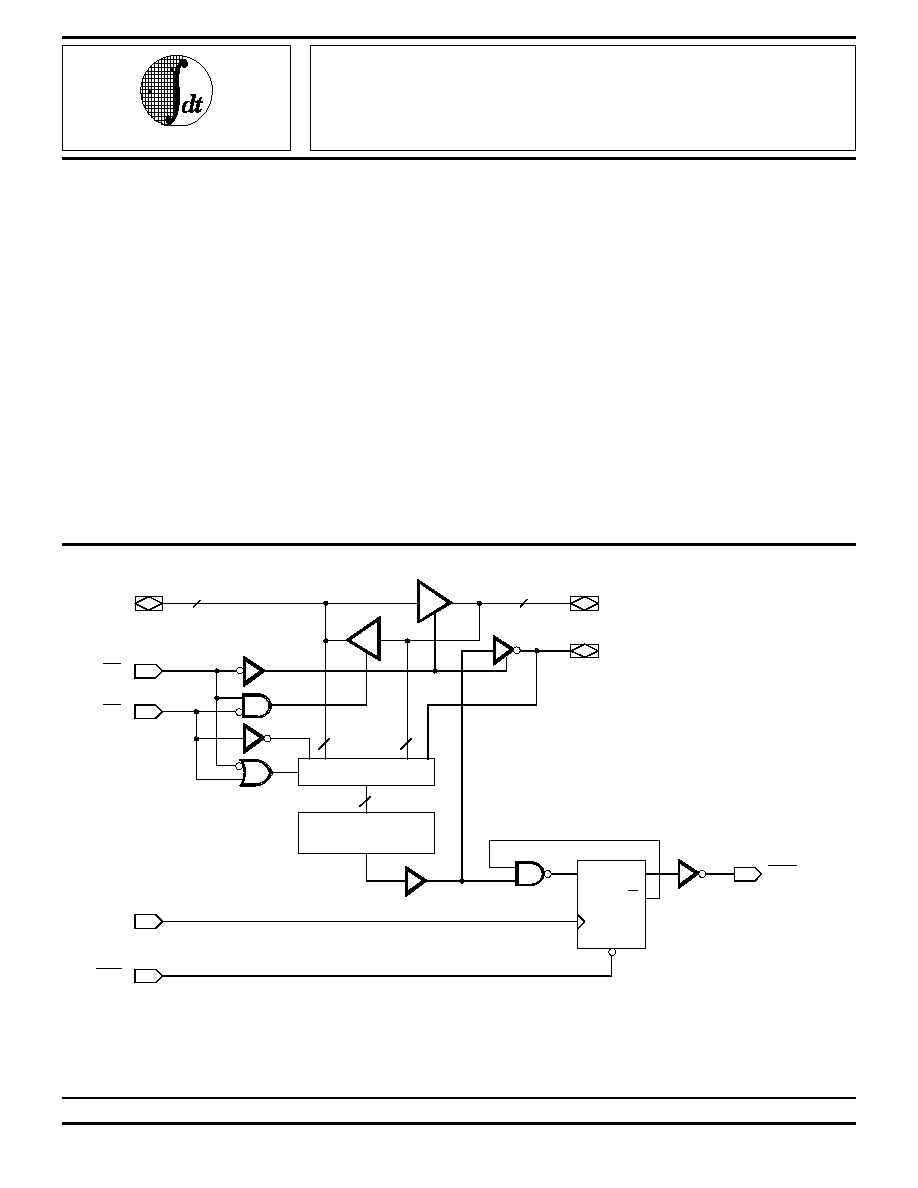
The IDT54/74FCT833s are high-performance bus
transceivers designed for two-way communications. They
each contain an 8-bit data path from the R (port) to the T (port),
an 8-bit data path from the T (port) to the R (port), and a 9-bit
parity checker/generator. The error flag can be clocked and
stored in a register and read at the
ERR
output. The clear
(
CLR
) input is used to clear the error flag register.
The output enables
OE
T
and
OE
R
are used to force the
port outputs to the high-impedance state so that the device
can drive bus lines directly. In addition,
OE
R
and
OE
T
can be
used to force a parity error by enabling both lines
simultaneously. This transmission of inverted parity gives the
designer more system diagnostic capability. The devices are
specified at 48mA and 32mA output sink current over the
commercial and military temperature ranges, respectively.
The IDT logo is a registered trademark of Integrated Device Technology, Inc.
FUNCTIONAL BLOCK DIAGRAM
OE
T
S
MUX
OE
R
9-BIT
PARITY TREE
9
8
R
I
8
8
T
D
CLR
CP
Q
Q
PARITY
CLK
CLR
ERR
2557 drw 01
P
8
I
IDT54/74FCT833A
IDT54/74FCT833B
1
7.21
2
IDT54/74FCT833A/B
FAST CMOS PARITY BUS TRANSCEIVER
MILITARY AND COMMERCIAL TEMPERATURE RANGES
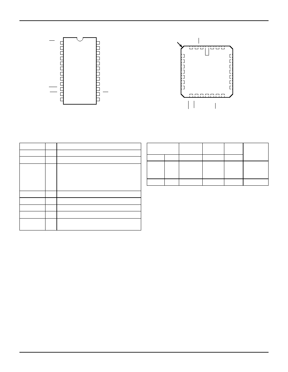
PIN CONFIGURATIONS
DIP/SOIC/CERPACK
TOP VIEW
LCC
TOP VIEW
2557 tbl 01
PIN DESCRIPTION
Pin Name
I/O
Description
OE
R
I
RECEIVE enable input.
R
I
I/O
8-bit RECEIVE data input/output.
ERR
O
Output from fault registers. Register
detection of odd parity fault on rising clock
edge (CLK). A registered
ERR
output
remains LOW until cleared. Open drain
output, requires pull up resistor.
CLR
I
Clears the fault register output.
T
I
I/O
8-bit TRANSMIT data input/output.
PARITY
I/O
1-bit PARITY output.
OE
T
I
TRANSMIT enable input.
CLK
I
External clock pulse input for fault register
flag.
ERROR FLAG OUTPUT FUNCTION TABLE
(1,2)
Internal
Output
Inputs
To Device
Pre-State
Output
CLR
CLR
CLK
Point "P"
ERR
ERR
n≠1
ERR
ERR
Function
H
H
H
H
Sample
H
--
L
L
(1's
H
L
--
L
Capture)
L
--
--
--
H
Clear
NOTES:
2557 tbl 02
1.
OE
T
is HIGH and
OE
R
is LOW.
2. H = HIGH
L = LOW
= LOW-to-HIGH transition of clock
≠ = Don't Care or Irrelevant
5
6
7
8
9
10
11
12
GND
R
1
R
2
R
3
1
2
3
4
24
23
22
21
20
19
18
17
Vcc
16
15
14
13
OE
P24-1,
D24-1,
S024-2
&
E24-1
T
1
R
4
R
5
R
6
T
2
T
3
T
4
T
5
CLK
CLR
OE
ERR
PARITY
T
T
6
T
7
T
0
R
R
7
R
0
5
6
7
8
9
10
11
L28-1
25
24
23
22
21
20
19
12 13 14 15 16 17 18
4
3
2
1
28 27 26
INDEX
2557 drw 02
R
2
R
3
R
4
R
5
R
6
T
2
T
3
T
4
T
5
T
6
T
7
R
7
NC
NC
R
1
Vcc
OE
T
1
T
0
R
R
0
NC
GND
CLK
CLR
OE
ERR
PARITY
T
NC
IDT54/74FCT833A/B
FAST CMOS PARITY BUS TRANSCEIVER
MILITARY AND COMMERCIAL TEMPERATURE RANGES
7.21
3
FUNCTION TABLE
(2)
Inputs
Outputs
T
I
Incl Parity
OE
OE
T
OE
OE
R
CLR
CLR
CLK
R
I
(
or H's)
(
of H's)
R
I
T
I
Parity
ERR
ERR
(1)
Function
L
H
H
H (Odd)
NA
NA
H
L
H
Transmit data from R Port
L
H
H
H (Even)
NA
NA
H
H
L
to T Port with parity;
L
H
H
L (Odd)
NA
NA
L
L
H
receiving path is disabled.
L
H
H
L (Even)
NA
NA
L
H
L
H
L
H
NA
H (Odd)
H
NA
NA
H
Receive data from T Port
H
L
H
NA
H (Even)
H
NA
NA
L
to R Port with parity test
H
L
H
NA
L (Odd)
L
NA
NA
H
resulting in flag:
H
L
H
NA
L (Even)
L
NA
NA
L
transmitting path is disabled.
--
--
L
--
--
--
NA
NA
NA
H
Clear the state of error flag
register.
H
H
H
H or L
--
--
Z
Z
Z
*
Both transmitting and
H
H
L
--
--
--
Z
Z
Z
H
receiving paths are disabled.
H
H
H
H or L (Odd)
--
Z
Z
Z
H
Parity logic defaults to
H
H
H
H or L (Even)
--
Z
Z
Z
L
transmit mode.
L
L
H
H (Odd)
NA
NA
H
H
L
Forced-error checking.
L
L
H
H (Even)
NA
NA
H
L
H
L
L
H
L (Odd)
NA
NA
L
H
L
L
L
H
L (Even)
NA
NA
L
L
H
NOTES:
2557 tbl 03
1. Output state assumes HIGH output pre-state.
2. H
=
HIGH
Z
=
High Impedance
Odd =
Odd number of logic one's
L
=
LOW
NA =
Not Applicable
Even =
Even number of logic one's
=
LOW-to-HIGH transition of clock
≠
=
Don't Care or Irrelevant
I
=
0, 1, 2, 3, 4, 5, 6, 7
*No change to stored Error State
7.21
4
IDT54/74FCT833A/B
FAST CMOS PARITY BUS TRANSCEIVER
MILITARY AND COMMERCIAL TEMPERATURE RANGES
DC ELECTRICAL CHARACTERISTICS OVER OPERATING RANGE
Following Conditions Apply Unless Otherwise Specified: V
LC
= 0.2V; V
HC
= V
CC
≠ 0.2V
Commercial: T
A
= 0
∞
C to +70
∞
C, V
CC
= 5.0V
±
5%; Military: T
A
= ≠55
∞
C to +125
∞
C, V
CC
= 5.0V
±
10%
Symbol
Parameter
Test Conditions
(1)
Min.
Typ.
(2)
Max.
Unit
V
IH
Input HIGH Level
Guaranteed Logic HIGH Level
2.0
--
--
V
V
IL
Input LOW Level
Guaranteed Logic LOW Level
--
--
0.8
V
I
IH
Input HIGH Current
V
CC
= Max.
V
I
=V
CC
--
--
5
µ
A
(Except I/O Pins)
V
I
= 2.7V
--
--
5
(4)
I
IL
Input LOW Current
V
I
= 0.5V
--
--
≠5
(4)
(Except I/O Pins)
V
I
= GND
--
--
≠5
I
IH
Input HIGH Current
V
CC
= Max.
V
I
= V
CC
--
--
15
µ
A
(I/O Pins Only)
V
I
= 2.7V
--
--
15
(4)
I
IL
Input LOW Current
V
I
= 0.5V
--
--
≠15
(4)
(I/O Pins Only)
V
I
= GND
--
--
≠15
V
IK
Clamp Diode Voltage
Vcc = Min., I
N
= ≠18mA
--
≠0.7
≠1.2
V
I
OS
Short Circuit Current
Vcc = Max.
(3)
, V
O
= GND
≠60
≠120
--
mA
V
OH
Output HIGH Voltage
Vcc = 3V, V
IN
= V
LC
or V
HC
, I
OH
= ≠32
µ
A
V
HC
V
CC
--
V
(Except
ERR
)
Vcc = Min.
I
OH
= ≠300
µ
A
V
HC
V
CC
--
V
IN
= V
IH
or V
IL
I
OH
= ≠15mA MIL.
2.4
4.3
--
I
OH
= ≠24mA COM'L.
2.4
4.3
--
V
OL
Output LOW Voltage
Vcc = 3V, V
IN
= V
LC
or V
HC
, I
OL
= 300
µ
A
--
GND
V
LC
V
Vcc = Min.
Except
I
OL
= 300
µ
A
--
GND
V
LC
(4)
V
IN
= V
IH
ERR
I
OL
= 32 mA MIL.
--
0.3
0.5
or V
IL
I
OL
= 48mA COM'L.
--
0.3
0.5
ERR
I
OL
= 48mA
--
0.3
0.5
NOTES:
2557 tbl 06
1. For conditions shown as Max. or Min., use appropriate value specified under Electrical Characteristics for the applicable device type.
2. Typical values are at V
CC
= 5.0V, +25
∞
C ambient and maximum loading.
3. Not more than one output should be shorted at one time. Duration of the short circuit test should not exceed one second.
4. This parameter is guaranteed but not tested.
ABSOLUTE MAXIMUM RATINGS
(1)
Symbol
Rating
Commercial
Military
Unit
V
TERM
(2)
Terminal Voltage
≠0.5 to +7.0 ≠0.5 to +7.0
V
with Respect
to GND
V
TERM
(3)
Terminal Voltage
≠0.5 to V
CC
≠0.5 to V
CC
V
with Respect
to GND
T
A
Operating
0 to +70
≠55 to +125
∞
C
Temperature
T
BIAS
Temperature
≠55 to +125 ≠65 to +135
∞
C
Under Bias
T
STG
Storage
≠55 to +125 ≠65 to +150
∞
C
Temperature
P
T
Power Dissipation
0.5
0.5
W
I
OUT
DC Output Current
120
120
mA
NOTES:
2557 tbl 03
1. Stresses greater than those listed under ABSOLUTE MAXIMUM RATINGS
may cause permanent damage to the device. This is a stress rating only
and functional operation of the device at these or any other conditions
above those indicated in the operational sections of this specification is
not implied. Exposure to absolute maximum rating conditions for
extended periods may affect reliability. No terminal voltage may exceed
V
CC
by +0.5V unless otherwise noted.
2. Inputs and V
CC
terminals.
3. Outputs and I/O terminals.
CAPACITANCE
(T
A
= +25
∞
C, f = 1.0MHz)
Symbol Parameter
(1)
Conditions
Typ.
Max.
Unit
C
IN
Input
V
IN
= 0V
6
10
pF
Capacitance
C
I/O
I/O
V
OUT
= 0V
8
12
pF
Capacitance
NOTE:
2557 tbl 05
1. This parameter is guaranteed by characterization but not tested.
IDT54/74FCT833A/B
FAST CMOS PARITY BUS TRANSCEIVER
MILITARY AND COMMERCIAL TEMPERATURE RANGES
7.21
5
POWER SUPPLY CHARACTERISTICS
V
LC
= 0.2V; V
HC
= V
CC
≠ 0.2V
Symbol
Parameter
Test Conditions
(1)
Min.
Typ.
(2)
Max.
Unit
I
CC
Quiescent Power Supply Current
Vcc = Max.; V
IN
V
HC
, V
IN
V
LC
--
0.2
1.5
mA
I
CC
Quiescent Power Supply Current
Vcc = Max.
--
0.5
2.0
mA
TTL Inputs HIGH
V
IN
= 3.4V
(3)
I
CCD
Dynamic Power Supply Current
(4)
Vcc = Max.
V
IN
V
HC
--
0.15
0.25
mA/
Outputs Open
V
IN
V
LC
MHz
OE
T
=
OE
R
= GND
One Input Toggling
50% Duty Cycle
I
C
Total Power Supply Current
(6)
Vcc = Max.
V
IN
V
HC
--
1.4
3.4
mA
Outputs Open
V
IN
V
LC
f
CP
= 10MHz
(FCT)
50% Duty Cycle
OE
T
= GND
V
IN
= 3.4V
--
1.9
5.4
OE
R
= V
CC
V
IN
= GND
f
i
= 2.5MHz
One Bit Toggling
Vcc = Max.
V
IN
V
HC
--
4.0
7.8
(5)
Outputs Open
V
IN
V
LC
f
CP
= 10MHz
(FCT)
50% Duty Cycle
OE
T
= GND
V
IN
= 3.4V
--
6.2
16.8
(5)
f
i
= 2.5MHz
V
IN
= GND
OE
R
= V
CC
Eight Bits Toggling
NOTES:
2557 tbl 07
1. For conditions shown as Max. or Min., use appropriate value specified under Electrical Characteristics for the applicable device type.
2. Typical values are at V
CC
= 5.0V, +25
∞
C ambient.
3. Per TTL driven input (V
IN
= 3.4V); all other inputs at V
CC
or GND.
4. This parameter is not directly testable, but is derived for use in Total Power Supply calculations.
5. Values for these conditions are examples of the I
CC
formula. These limits are guaranteed but not tested.
6. I
C
= I
QUIESCENT
+ I
INPUTS
+ I
DYNAMIC
I
C
= I
CC
+
I
CC
D
H
N
T
+ I
CCD
(f
CP
/2 + f
i
N
i
)
I
CC
= Quiescent Current
I
CC
= Power Supply Current for a TTL High Input (V
IN
= 3.4V)
D
H
= Duty Cycle for TTL Inputs High
N
T
= Number of TTL Inputs at D
H
I
CCD
= Dynamic Current Caused by an Output Transition Pair (HLH or LHL)
f
CP
= Clock Frequency for Register Devices (Zero for Non-Register Devices)
f
i
= Input Frequency
N
i
= Number of Inputs at f
i
All currents are in milliamps and all frequencies are in megahertz.

7.21
6
IDT54/74FCT833A/B
FAST CMOS PARITY BUS TRANSCEIVER
MILITARY AND COMMERCIAL TEMPERATURE RANGES
SWITCHING CHARACTERISTICS OVER OPERATING RANGE
IDT54/74FCT833A
IDT54/74FCT833B
Com'l.
Mil.
Com'l.
Mil.
Symbol
Parameter
Conditions
(1)
Min.
(2)
Max.
Min.
(2)
Max.
Min.
(2)
Max.
Min.
(2)
Max.
Unit
t
PLH
Propagation Delay
C
L
= 50pF
--
10.0
--
14.0
--
7.0
--
10.0
ns
t
PHL
R
I
to T
I
, T
I
to R
I
C
L
= 300pF
(3)
--
17.5
--
21.5
--
14.5
--
17.5
t
PLH
Propagation Delay
C
L
= 50pF
--
15.0
--
20.0
--
10.5
--
14.0
ns
t
PHL
R
I
to PARITY
C
L
= 300pF
(3)
--
22.5
--
27.5
--
18.0
--
21.5
t
PZH
Output Enable Time
C
L
= 50pF
--
12.0
--
16.0
--
8.5
--
11.0
ns
t
PZL
OE
R
,
OE
T
to R
I
, T
I
C
L
= 300pF
(3)
--
19.5
--
23.5
--
16.0
--
18.5
t
PHZ
Output Disable Time C
L
= 5pF
(3)
--
10.7
--
14.7
--
7.2
--
9.8
ns
t
PLZ
OE
R
,
OE
T
to R
I
, T
I
C
L
= 50pF
--
12.0
--
16.0
--
8.5
--
11.0
t
SU
T
I
, PARITY to CLK
C
L
= 50pF
12.0
--
16.0
--
8.5
--
11.0
--
ns
Set-up Time
t
H
T
I
, PARITY to CLK
0
--
0
--
0
--
0
--
ns
Hold Time
t
REM
Clear Recovery Time
15.0
--
20.0
--
10.5
--
14.0
--
ns
CLR
to CLK
t
W
Clock Pulse Width
7.0
--
9.5
--
5.5
--
7.0
--
ns
HIGH or LOW
t
W
Clear Pulse Width
7.0
--
9.5
--
5.5
--
7.0
--
ns
LOW
t
PHL
Propagation Delay
--
12.0
--
16.0
--
8.5
--
11.0
ns
CLK to
ERR
t
PLH
Propagation Delay
--
16.0
--
20.0
--
15.0
--
18.0
ns
CLR
to
ERR
t
PLH
Propagation Delay
C
L
= 50pF
--
15.0
--
20.0
--
10.5
--
14.0
ns
t
PHL
OE
R
to PARITY
C
L
= 300pF
(3)
--
22.5
--
27.5
--
18.0
--
21.5
NOTES:
2557 tbl 08
1. See test circuit and waveforms.
2. Minimum limits are guaranteed but not tested on Propagation Delays.
3. These parameters are guaranteed but not tested.
IDT54/74FCT833A/B
FAST CMOS PARITY BUS TRANSCEIVER
MILITARY AND COMMERCIAL TEMPERATURE RANGES
7.21
7
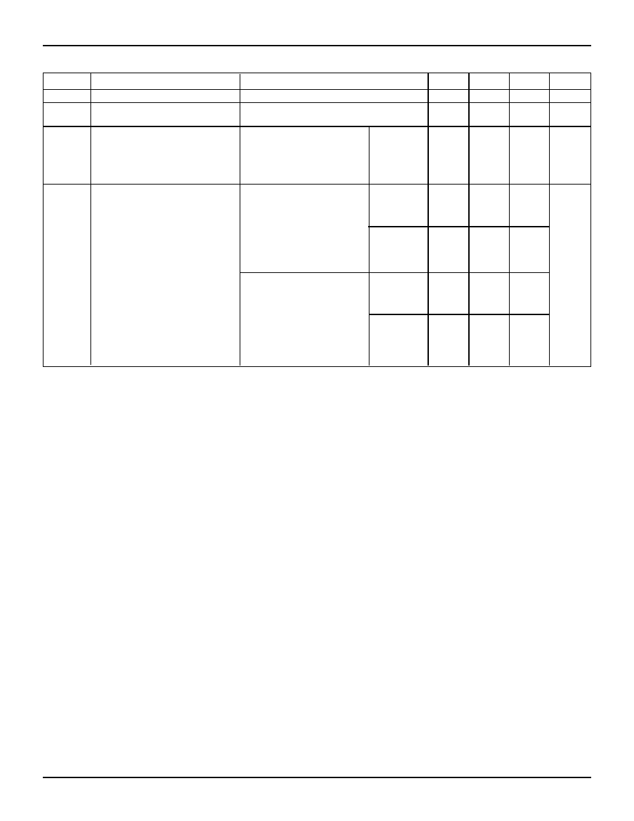
TEST CIRCUITS AND WAVEFORMS
TEST CIRCUITS FOR ALL OUTPUTS
ENABLE AND DISABLE TIMES
PROPAGATION DELAY
SET-UP, HOLD AND RELEASE TIMES
PULSE WIDTH
Pulse
Generator
DATA
INPUT
TIMING
INPUT
ASYNCHRONOUS CONTROL
PRESET
CLEAR
ETC.
SYNCHRONOUS CONTROL
PRESET
CLEAR
CLOCK ENABLE
ETC.
3V
1.5V
0V
3V
1.5V
0V
3V
1.5V
0V
3V
1.5V
0V
t
SU
t
H
t
REM
H
t
SU
R
T
D.U.T.
V
CC
V
IN
C
L
V
OUT
50pF
500
500
7.0V
SAME PHASE
INPUT TRANSITION
3V
1.5V
0V
1.5V
V
OH
V
OL
t
PLH
t
PHL
OUTPUT
OPPOSITE PHASE
INPUT TRANSITION
CONTROL
INPUT
3V
1.5V
0V
3.5V
0V
OUTPUT
NORMALLY
LOW
OUTPUT
NORMALLY
HIGH
SWITCH
CLOSED
SWITCH
OPEN
V
OL
V
OH
3V
1.5V
0V
t
PLH
t
PHL
0.3V
0.3V
t
PLZ
t
PZL
t
PZH
t
PHZ
3.5V
0V
1.5V
1.5V
ENABLE
DISABLE
HIGH-LOW-HIGH
PULSE
LOW-HIGH-LOW
PULSE
t
W
1.5V
1.5V
t
NOTES
2557 drw 04
1. Diagram shown for input Control Enable-LOW and input Control
Disable-HIGH.
2. Pulse Generator for All Pulses: Rate
1.0 MHz; Z
O
50
; t
F
2.5ns;
t
R
2.5ns.
SWITCH POSITION
Test
Switch
Open Drain
Disable Low
Closed
Enable Low
All Other Tests
Open
DEFINITIONS:
2557 tbl 09
C
L
= Load capacitance: includes jig and probe capacitance.
R
T
= Termination resistance: should be equal to Z
OUT
of the Pulse
Generator.
7.21
8
IDT54/74FCT833A/B
FAST CMOS PARITY BUS TRANSCEIVER
MILITARY AND COMMERCIAL TEMPERATURE RANGES
ORDERING INFORMATION
X
Package
X
Process/
Temperature
Range
Blank
B
Commercial (0
∞
C to +70
∞
C)
Military (≠55
∞
C to +125
∞
)
Compliant to MIL-STD-883, Class B
P
D
L
SO
E
Plastic DIP
CERDIP
Leadless Chip Carrier
Small Outline IC
CERPACK
833A
833B
Non-inverting Parity Bus Transceiver
Fast Non-inverting Parity Bus Transceiver
X
Device
Type
2557 drw 03
54
75
≠55
∞
C to +125
∞
C
0
∞
C to +70
∞
C
XXX
Temperature
Range
FCT
IDT