
1
INDUSTRIAL TEMPERATURE RANGE
IDT5V2528/A
2.5 / 3.3V PHASE-LOCK LOOP CLOCK DRIVER
JUNE 2003
2002 Integrated Device Technology, Inc.
DSC 5971/11
c
INDUSTRIAL TEMPERATURE RANGE
The IDT logo is a registered trademark of Integrated Device Technology, Inc.
FEATURES:
∑ Operates at 3.3V V
DD
/AV
DD
and 2.5V/3.3V V
DDQ
∑ 1:10 fanout
∑ 3-level inputs for output control
∑ External feedback (FBIN) pin is used to synchronize the
outputs to the clock input signal
∑ No external RC network required for PLL loop stability
∑ Configurable 2.5V or 3.3V LVTTL outputs
∑ t
PD
Phase Error at 100MHz to 166MHz: ±150ps
∑ Jitter (peak-to-peak) at 133MHz and 166MHz: ±75ps
∑ Spread spectrum compatible
∑ Operating Frequency:
--
--
-
Std: 25MHz to 140MHz
--
--
- A: 25MHz to 167MHz
∑ Available in TSSOP package
FUNCTIONAL BLOCK DIAGRAM
DESCRIPTION:
The IDT5V2528 is a high performance, low-skew, low-jitter, phase-lock
loop (PLL) clock driver. It uses a PLL to precisely align, in both frequency
and phase, the feedback (FBOUT) output to the clock (CLK) input signal.
IDT5V2528/A
2.5V / 3.3V PHASE-LOCK
LOOP CLOCK DRIVER
ZERO DELAY BUFFER
19
Y1, V
DD
pin 21
PLL
3
24
17
16
26
TY0, V
DDQ
pin 4
13
10
20
12
Y0, V
DD
pin 21
6
7
5
AV
DD
FBIN
CLK
G_Ctrl
28
22
FBOUT, V
DD
pin 21
T_Ctrl
1
MODE
SELECT
TY1, V
DDQ
pin 25
TY2, V
DDQ
pin 25
TY3, V
DDQ
pin 15
TY4, V
DDQ
pin 15
TY5, V
DDQ
pin 11
TY6, V
DDQ
pin 11
TY7, V
DDQ
pin 11
The IDT5V2528 inputs, PLL core, Y
0
, Y
1
, and FB
OUT
buffers operate from
the 3.3V V
DD
and AV
DD
power supply pins.
One bank of ten outputs provide low-skew, low-jitter copies of CLK. Of
the ten outputs, up to seven may be configured for 2.5V or 3.3V LVTTL
outputs. The number of 2.5V outputs is controlled by 3-level input signals
G_Ctrl and T_Ctrl, and by connecting the appropriate V
DDQ
pins to 2.5V or
3.3V. The 3-level input signals may be hard-wired to high-mid-low levels.
Output signal duty cycles are adjusted to 50 percent, independent of the duty
cycle at CLK. The outputs can be enabled or disabled via the G_Ctrl input.
When the G_Ctrl input is mid or high, the outputs switch in phase and
frequency with CLK; when the G_Ctrl is low, all outputs (except FB
OUT
) are
disabled to the logic-low state.
Unlike many products containing PLLs, the IDT5V2528 does not require
external RC networks. The loop filter for the PLL is included on-chip,
minimizing component count, board space, and cost.
Because it is based on PLL circuitry, the IDT5V2528 requires a
stabilization time to achieve phase lock of the feedback signal to the
reference signal. This stabilization time is required, following power up and
application of a fixed-frequency, fixed-phase signal at CLK, as well as
following any changes to the PLL reference or feedback signals. The PLL
can be bypassed for test purposes by strapping AV
DD
to ground.

2
INDUSTRIAL TEMPERATURE RANGE
IDT5V2528/A
2.5 / 3.3V PHASE-LOCK LOOP CLOCK DRIVER
PIN CONFIGURATION
TSSOP
TOP VIEW
G_Ctrl
GND
TY1
V
DDQ
TY2
GND
FBOUT
V
DD
Y0
Y1
GND
TY3
V
DDQ
TY6
T_Ctrl
GND
TY0
V
DDQ
AV
DD
CLK
FBIN
AGND
GND
TY7
28
27
26
25
24
23
22
21
20
19
1
2
3
4
5
6
7
8
9
10
TY4
V
DDQ
TY5
GND
18
17
11
12
16
15
13
14
Symbol
Rating
Max.
Unit
V
DD,
V
DDQ,
AV
DD
Supply Voltage Range
≠0.5 to +4.6
V
V
I (2)
Input Voltage Range
≠0.5 to +5.5
V
V
O(2)
Voltage Range applied to any
≠0.5 to
V
output in the HIGH or LOW state V
DD
+0.5
I
IK
(V
I
< 0)
Input Clamp Current
≠50
mA
I
OK
Output Clamp Current
±50
mA
(V
O
< 0 or V
O
> V
DD
)
I
O
Continuous Output Current
±50
mA
(V
O
= 0 to V
DD
)
V
DD
or GND
Continuous Current
±200
mA
T
STG
Storage Temperature Range
≠65 to +150
∞C
T
J
Junction Temperature
+150
∞C
NOTES:
1. Stresses greater than those listed under ABSOLUTE MAXIMUM RATINGS may cause
permanent damage to the device. This is a stress rating only and functional operation
of the device at these or any other conditions above those indicated in the operational
sections of this specification is not implied. Exposure to absolute maximum rating
conditions for extended periods may affect reliability.
2. The input and output negative-voltage ratings may be exceeded if the input and output
clamp-current ratings are observed.
3. The maximum package power dissipation is calculated using a junction temperature
of 150
∞
C and a board trace length of 750 mils.
ABSOLUTE MAXIMUM RATINGS
(1)
Symbol
Description
Min.
Typ.
Max.
Unit
V
DD,
AV
DD (1)
Power Supply Voltage
3
3.3
3.6
V
V
DDQ (1)
Power Supply Voltage
2.5V Outputs
2.3
2.5
2.7
V
3.3V Outputs
3
3.3
3.6
T
A
Ambient Operating Temperature
≠40
+25
+85
∞C
RECOMMENDED OPERATING RANGE
Symbol
Description
Min
Typ.
Max. Unit
C
IN
Input Capacitance
--
5
--
pF
V
I
= V
DD
or GND
C
O
Output Capacitance
--
6
--
pF
V
I
= V
DD
or GND
C
L
Load Capacitance
2.5V outputs --
20
--
pF
3.3V outputs --
30
--
CAPACITANCE
(1)
NOTE:
1. Unused inputs must be held HIGH or LOW to prevent them from floating.
NOTE:
1. All power supplies should operate in tandem. If V
DD
or V
DDQ
is at a maximum, then V
DDQ
or V
DD
(respectively) should be at maximum, and vice-versa.
3
INDUSTRIAL TEMPERATURE RANGE
IDT5V2528/A
2.5 / 3.3V PHASE-LOCK LOOP CLOCK DRIVER
PIN DESCRIPTION
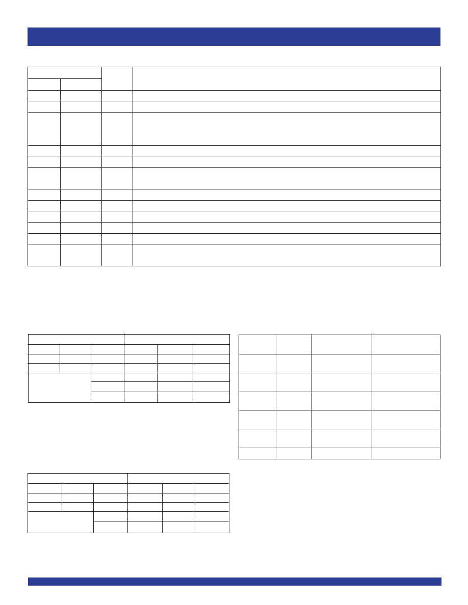
Terminal
Name
No.
Type
Description
CLK
(1)
6
I
Clock input
FBIN
7
I
Feedback input
G_Ctrl
(2)
28
3-level
3-level input for 2.5V / 3.3V Output Select/ Output bank enable. When G_Ctrl is LOW, all outputs except FBOUT are disabled
to a logic-LOW state. When G_Ctrl is MID or HIGH, all outputs are enabled and switch at the same frequency as CLK (see
OUTPUT SELECTION table).
T_Ctrl
(2)
1
3-level
3-level input for 2.5V / 3.3V Output Select (see OUTPUT SELECTION table)
FBOUT
22
O
Feedback output
TY
(7:0)
3, 10, 12, 13,
O
2.5V or 3.3V Clock outputs. 1, 2, 3, 5, or 7 of these outputs may be selected as 2.5V outputs (see OUTPUT SELECTION table).
16, 17, 24, 26
Y
(1:0)
19, 20
O
3.3V Clock Outputs
AV
DD(3)
5
Power
3.3V Analog power supply. AV
DD
provides the power reference for the analog circuitry.
AGND
8
Ground
Analog ground. AGND provides the ground reference for the analog circuitry.
V
DD
21
Power
3.3V Power supply
V
DDQ
4, 11, 15, 25
Power
2.5V or 3.3V Power supply for TY outputs
GND
2, 9, 14, 18
Ground
Ground
23, 27
NOTES:
1. CLK must have a fixed frequency and fixed phase for the PLL to obtain phase lock. Once the circuit is powered up and a valid CLK signal is applied, a stabilization time of 1ms
is required for the PLL to phase lock the feedback signal to the reference signal.
2. 3-level inputs will float to MID logic level if left unconnected.
3. AV
DD
can be used to bypass the PLL for test purposes. When AV
DD
is strapped to ground, PLL is bypassed and CLK is buffered directly to the outputs.
OUTPUT SELECTION
V
DDQ
G_Ctrl
T_Ctrl
TY
(7:0)
Configuration
M
L
TY
0
(2.5V)
Pin 4 (2.5V)
TY
1
- TY
7
(3.3V)
Pins 11, 15, 25 (3.3V)
M
M
TY
1,
TY
2
(2.5V)
Pin 25 (2.5V)
TY
0,
TY
3
- TY
7
(3.3V)
Pins 4, 11, 15 (3.3V)
M
H
TY
0
- TY
2
(2.5V)
Pins 4, 25 (2.5V)
TY
3
- TY
7
(3.3V)
Pins 11, 15 (3.3V)
H
L
TY
0
- TY
4
(2.5V)
Pins 4, 15, 25 (2.5V)
TY
5
- TY
7
(3.3V)
Pin 11 (3.3V)
H
M
TY
1
- TY
7
(2.5V)
Pins 11, 15, 25 (2.5V)
TY
0
(3.3V)
Pin 4 (3.3V)
H
H
TY
o
- TY
7
(3.3V)
Pins 4, 11, 15, 25 (3.3V)
STATIC FUNCTION TABLE
(A
VDD
= 0V)
(1)
Inputs
Outputs
G_Ctrl
T_Ctrl
CLK
TY
(7:0)
Y
(1:0)
FBOUT
L
X
L
L
L
L
L
X
H
L
L
H
see
H
H
H
H
OUTPUT SELECTION
L
L
L
L
table
running
running
running
running
DYNAMIC FUNCTION TABLE
(A
VDD
= 3.3V)
Inputs
Outputs
G_Ctrl
T_Ctrl
CLK
TY
(7:0)
Y
(1:0)
FBOUT
L
X
L
L
L
L
L
X
H
L
L
H
see OUTPUT
L
L
L
L
SELECTION table
H
H
H
H
NOTE:
1. AV
DD
should be powered up along with V
DD
, before setting AV
DD
to ground, to put the
control pins in a valid state.

4
INDUSTRIAL TEMPERATURE RANGE
IDT5V2528/A
2.5 / 3.3V PHASE-LOCK LOOP CLOCK DRIVER
DC ELECTRICAL CHARACTERISTICS OVER OPERATING RANGE
Symbol
Parameter
Test Conditions
Min.
Typ.
(1)
Max
Unit
V
IK
Input Clamp Voltage
I
I
= -18mA
- 1.2
V
V
IH
Input HIGH Level
CLK, FBIN
2
V
V
IL
Input LOW Level
CLK, FBIN
0.8
V
V
IHH
Input HIGH Voltage Level
(2)
3-Level Inputs Only
V
DD
- 0.6
V
V
IMM
Input MID Voltage Level
(2)
3-Level Inputs Only
V
DD
/2 - 0.3
V
DD
/2 + 0.3
V
V
ILL
Input LOW Voltage Level
(2)
3-Level Inputs Only
0.6
V
V
OH
Output HIGH Voltage Level
I
OH
= -100
µA
V
DD
- 0.2
V
(3.3V Outputs)
I
OH
= -12mA
2.4
V
OH
Output HIGH Voltage Level
I
OH
= -100
µA
V
DD
- 0.1
(2.5V Outputs)
I
OH
= -12mA
2
V
V
OL
Output LOW Voltage Level
I
OL
= 100
µA
0.2
V
(3.3V Outputs)
I
OL
= 12mA
0.4
V
OL
Output LOW Voltage Level
I
OL
= 100
µA
0.1
V
(2.5V Outputs)
I
OL
= 12mA
0.4
I
3
3-Level Input DC Current
V
IN
= V
DD
HIGH Level
+200
(G_Ctrl, T_Ctrl)
V
IN
= V
DD
/2
MID Level
≠50
+50
µA
V
IN
= GND
LOW Level
≠200
I
I
Input Current
V
I
= V
DD
or GND
±5
µA
NOTES:
1. For conditions shown as Min or Max, use the appropriate value specified under recommended operating conditions.
2. These inputs are normally wired to V
DD
, GND, or left floating. Internal termination resistors bias floating inputs to V
DD
/2. If these inputs are switched, the function and timing of
the outputs may be glitched, and the PLL may require an additional t
LOCK
time before all datasheet limits are achieved.
POWER SUPPLY CHARACTERISTICS
Symbol
Parameter
Test Conditions
Typ.
(1)
Max
Unit
I
DDPD
Power Down Supply Current
V
DD
= 3.6, V
DDQ
= 2.7V / 3.3V, AV
DD
= 0V
8
40
µA
I
DDA
AV
DD
Supply Current
V
DD
= AV
DD
= 3.6V, V
DDQ
= 2.7V / 3.3V, CLK = 0 or V
DD
3.5
10
mA
I
DD
Dynamic Power Supply Current
V
DD
= AV
DD
= 3.6V, V
DDQ
= 2.7V / 3.3V, C
L
= 0pF
500
--
µA/MHz
V
DD
= AV
DD
= V
DDQ
= 3.6V
15
--
I
DDD
Dynamic Power Supply
C
L
= 30pF, CLK = 100MHz
mA
Current per Output
V
DD
= AV
DD
= 3.6V, V
DDQ
= 2.7V
12
--
C
L
= 20pF, CLK = 100MHz
NOTE:
1. For nominal voltage and temperature.

5
INDUSTRIAL TEMPERATURE RANGE
IDT5V2528/A
2.5 / 3.3V PHASE-LOCK LOOP CLOCK DRIVER
INPUT TIMING REQUIREMENTS OVER OPERATING RANGE
5V2528
5V2528A
Min
Max
Min
Max
Units
f
CLOCK
Clock frequency
25
140
25
167
MHz
Input clock duty cycle
40%
60%
40%
60%
t
LOCK
Stabilization time
(1)
1
1
ms
NOTE:
1.Time required for the integrated PLL circuit to obtain phase lock of its feedback signal to its reference signal. For phase lock to be obtained, a fixed-frequency, fixed-phase reference
signal must be present at CLK. Until phase lock is obtained, the specifications for propagation delay, skew, and jitter parameters given in the switching characteristics table are
not applicable.
NOTES:
1. All parameters are measured with the following load conditions: 30pF || 500
for 3.3V outputs and 20pF || 500 for 2.5V outputs.
2. The specifications for parameters in this table are applicable only after any appropriate stabilization time has elapsed.
3. Phase error does not include jitter.
4. All skew parameters are only valid for equal loading of all outputs.
5. Measured for V
DDQ
= 2.3V and 3V, 2.5V and 3.3V, or 2.7V and 3.6V.
SWITCHING CHARACTERISTICS OVER OPERATING RANGE - 5V2528
(1)
Symbol
Parameter
(2)
Min.
Typ.
Max.
Unit
t
PHASE
error
Phase Error from Rising Edge CLK to Rising Edge FBIN (100MHz-133MHz)
≠
150
--
150
ps
t
PHASE
error - jitter
(3)
Phase Error minus Jitter from Rising Edge CLK to Rising Edge FBIN (133MHz)
≠
50
--
50
ps
t
SK
1(0)
(4)
Output Skew between 3.3V Outputs
--
--
150
ps
t
SK
2(0)
(4)
Output Skew between 2.5V Outputs
--
--
150
ps
t
SK
3(0)
(4,5)
Output Skew between 2.5V and 3.3V Outputs
--
--
200
ps
t
J
Cycle-to-Cycle Output Jitter (Peak-to-Peak) at 133MHz
≠
75
--
75
ps
Duty Cycle
45
--
55
%
t
R
Output Rise Time for 3.3V Outputs (20% to 80%)
0.8
--
2.1
ns
t
F
Output Fall Time for 3.3V Outputs (20% to 80%)
0.8
--
2.1
ns
t
R
Output Rise Time for 2.5V Outputs (20% to 80%)
0.5
--
1.5
ns
t
F
Output Fall Time for 2.5V Outputs (20% to 80%)
0.5
--
1.5
ns
SWITCHING CHARACTERISTICS OVER OPERATING RANGE - 5V2528A
(1)
Symbol
Parameter
(2)
Min.
Typ.
Max.
Unit
t
PHASE
error
Phase Error from Rising Edge CLK to Rising Edge FBIN (100MHz-166MHz)
≠
150
--
150
ps
t
PHASE
error - jitter
(3)
Phase Error minus Jitter from Rising Edge CLK to Rising Edge FBIN (166MHz)
≠
50
--
50
ps
t
SK
1(0)
(4)
Output Skew between 3.3V Outputs
--
--
150
ps
t
SK
2(0)
(4)
Output Skew between 2.5V Outputs
--
--
150
ps
t
SK
3(0)
(4,5)
Output Skew between 2.5V and 3.3V Outputs
25MHz to 133MHz
--
--
200
ps
133MHz to 166MHz
--
--
250
t
J
Cycle-to-Cycle Output Jitter (Peak-to-Peak) at 166MHz
≠
75
--
75
ps
Duty Cycle
45
--
55
%
t
R
Output Rise Time for 3.3V Outputs (20% to 80%)
0.8
--
2.1
ns
t
F
Output Fall Time for 3.3V Outputs (20% to 80%)
0.8
--
2.1
ns
t
R
Output Rise Time for 2.5V Outputs (20% to 80%)
0.5
--
1.5
ns
t
F
Output Fall Time for 2.5V Outputs (20% to 80%)
0.5
--
1.5
ns