1
COMMERCIAL AND INDUSTRIAL TEMPERATURE RANGES
IDT5V991A
3.3V PROGRAMMABLE SKEW PLL CLOCK DRIVER TURBOCLOCK
SEPTEMBER 2001
2001 Integrated Device Technology, Inc.
DSC 5963/3
c
IDT5V991A
COMMERCIAL AND INDUSTRIAL TEMPERATURE RANGES
3.3V PROGRAMMABLE
SKEW PLL CLOCK DRIVER
TURBOCLOCKTM
The IDT logo is a registered trademark of Integrated Device Technology, Inc.
FEATURES:
∑ REF is 5V tolerant
∑ 4 pairs of programmable skew outputs
∑ Low skew: 200ps same pair, 250ps all outputs
∑ Selectable positive or negative edge synchronization:
Excellent for DSP applications
∑ Synchronous output enable
∑ Output frequency: 3.75MHz to 85MHz
∑ 2x, 4x, 1/2, and 1/4 outputs
∑ 3 skew grades:
IDT5V991A-2: t
SKEW0
<250ps
IDT5V991A-5: t
SKEW0
<500ps
IDT5V991A-7: t
SKEW0
<750ps
∑ 3-level inputs for skew and PLL range control
∑ PLL bypass for DC testing
∑ External feedback, internal loop filter
∑ 12mA balanced drive outputs
∑ Low Jitter: <200ps peak-to-peak
∑ Available in 32-pin PLCC Package
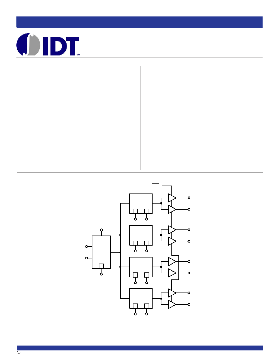
DESCRIPTION:
The IDT5V991A is a high fanout 3.3V PLL based clock driver intended
for high performance computing and data-communications applications. A
key feature of the programmable skew is the ability of outputs to lead or lag
the REF input signal. The IDT5V991A has eight programmable skew
outputs in four banks of 2. Skew is controlled by 3-level input signals that
may be hard-wired to appropriate HIGH-MID-LOW levels.
When the GND/
sOE pin is held low, all the outputs are synchronously
enabled. However, if GND/
sOE is held high, all the outputs except 3Q0 and
3Q1 are synchronously disabled.
Furthermore, when the V
CCQ
/PE is held high, all the outputs are
synchronized with the positive edge of the REF clock input. When V
CCQ
/
PE is held low, all the outputs are synchronized with the negative edge of
REF. Both devices have LVTTL outputs with 12mA balanced drive outputs.
FUNCTIONAL BLOCK DIAGRAM
GND/sOE
1Q
0
Skew
Select
1Q
1
1F1:0
3
3
2Q
0
Skew
Select
2Q
1
2F1:0
FS
3
REF
PLL
FB
3
3Q
0
Skew
Select
3Q
1
3F1:0
3
3
4Q
0
4Q
1
Skew
Select
4F1:0
3
3
3
V
CCQ
/PE
2
COMMERCIAL AND INDUSTRIAL TEMPERATURE RANGES
IDT5V991A
3.3V PROGRAMMABLE SKEW PLL CLOCK DRIVER TURBOCLOCK
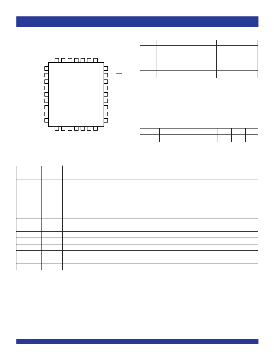
PIN CONFIGURATION
NOTE:
1. Stresses beyond those listed under ABSOLUTE MAXIMUM RATINGS may cause
permanent damage to the device. These are stress ratings only, and functional
operation of the device at these or any other conditions above those indicated in the
operational sections of this specification is not implied. Exposure to absolute-
maximum-rated conditions for extended periods may affect device reliability.
5
6
7
8
9
10
11
12
13
29
28
27
26
25
24
23
22
21
3F
1
4F
0
4F
1
V
CC Q
/PE
4Q
1
4Q
0
G ND
G ND
2F
0
GN D/sO E
1F
1
1F
0
1Q
0
1Q
1
GN D
GN D
4
3
2
1
32
31
30
14
15
16
17
18
19
20
3
F
0
F
S
R
E
F
G
N
D
T
E
S
T
2
F
1
3
Q
1
3
Q
0
F
B
2
Q
1
2
Q
0
V
C C N
V
C
C
N
V
C
C
N
V
C
C
Q
V
C C N
PLCC
TOP VIEW
Output skew with respect to the REF input is adjustable to compensate
for PCB trace delays, backplane propagation delays or to accommodate
requirements for special timing relationships between clocked compo-
nents. Skew is selectable as a multiple of a time unit t
U
which is of the
order of a nanosecond (see PLL Programmable Skew Range and Resolution
Table). There are nine skew configurations available for each output
pair. These configurations are chosen by the nF
1:0
control pins. In order
to minimize the number of control pins, 3-level inputs (HIGH-MID-LOW)
are used, they are intended for but not restricted to hard-wiring. Undriven
3-level inputs default to the MID level. Where programmable skew is
not a requirement, the control pins can be left open for the zero skew
default setting. The Control Summary Table shows how to select specific
skew taps by using the nF
1:0
control pins.
PROGRAMMABLE SKEW
ABSOLUTE MAXIMUM RATINGS
(1)
Symbol
Description
Max
Unit
Supply Voltage to Ground
≠0.5 to +7
V
V
I
DC Input Voltage
≠0.5 to V
CC
+0.5
V
REF Input Voltage
≠0.5 to +5.5
V
T
J
Junction Temperature
150
∞ C
T
STG
Storage Temperature
≠65 to +150
∞ C
NOTE:
1. Capacitance applies to all inputs except TEST, FS, and nF1:0.
CAPACITANCE
(T
A
= +25∞C, f = 1MHz, V
IN
= 0V)
Parameter
Description
Typ.
Max.
Unit
C
IN
Input Capacitance
5
7
pF
PIN DESCRIPTION
Pin Name
Type
Description
REF
I N
Reference Clock Input
FB
I N
Feedback Input
TEST
(1)
I N
When MID or HIGH, disables PLL (except for conditions of Note 1). REF goes to all outputs. Skew selections (see Control
Summary Table) remain in effect. Set LOW for normal operation.
GND/
sOE
(1)
I N
Synchronous Output Enable. When HIGH, it stops clock outputs (except 3Q
0
and 3Q
1
) in a LOW state - 3Q
0
and 3Q
1
may be used
as the feedback signal to maintain phase lock. When TEST is held at MID level and GND/
sOE is HIGH, the nF[
1:0
] pins act as
output disable controls for individual banks when nF[
1:0
] = LL. Set GND/
sOE LOW for normal operation.
V
CCQ
/PE
I N
Selectable positive or negative edge control. When LOW/HIGH the outputs are synchronized with the negative/positive edge of the
reference clock.
nF[
1:0
]
I N
3-level inputs for selecting 1 of 9 skew taps or frequency functions
FS
I N
Selects appropriate oscillator circuit based on anticipated frequency range. (See PLL Programmable Skew Range.)
nQ[
1:0
]
OUT
Four banks of two outputs with programmable skew
V
CCN
PWR
Power supply for output buffers
V
CCQ
PWR
Power supply for phase locked loop and other internal circuitry
GND
PWR
Ground
NOTE:
1.When TEST = MID and GND/
sOE = HIGH, PLL remains active with nF[
1:0
] = LL functioning as an output disable control for individual output banks. Skew selections remain
in effect unless nF[
1:0
] = LL.

3
COMMERCIAL AND INDUSTRIAL TEMPERATURE RANGES
IDT5V991A
3.3V PROGRAMMABLE SKEW PLL CLOCK DRIVER TURBOCLOCK
EXTERNAL FEEDBACK
By providing external feedback, the IDT5V991A gives users flexibility
with regard to skew adjustment. The FB signal is compared with the
input REF signal at the phase detector in order to drive the VCO. Phase
differences cause the VCO of the PLL to adjust upwards or downwards
accordingly.
NOTES:
1. The device may be operated outside recommended frequency ranges without damage, but functional operation is not guaranteed. Selecting the appropriate FS value based on
input frequency range allows the PLL to operate in its `sweet spot' where jitter is lowest.
2. The level to be set on FS is determined by the nominal operating frequency of the VCO and Time Unit Generator. The VCO frequency always appears at 1Q
1:0
, 2Q
1:0
, and the
higher outputs when they are operated in their undivided modes. The frequency appearing at the REF and FB inputs will be the same as the VCO when the output connected
to FB is undivided. The frequency of the REF and FB inputs will be 1/2 or 1/4 the VCO frequency when the part is configured for a frequency multiplication by using a divided
output as the FB input.
3. Skew adjustment range assumes that a zero skew output is used for feedback. If a skewed Q output is used for feedback, then adjustment range will be greater. For example
if a 4t
U
skewed output is used for feedback, all other outputs will be skewed ≠4t
U
in addition to whatever skew value is programmed for those outputs. `Max adjustment' range
applies to output pairs 3 and 4 where ± 6t
U
skew adjustment is possible and at the lowest F
NOM
value.
An internal loop filter moderates the response of the VCO to the
phase detector. The loop filter transfer function has been chosen to
provide minimal jitter (or frequency variation) while still providing accu-
rate responses to input frequency changes.
FS = LOW
FS = MID
FS = HIGH
Comments
Timing Unit Calculation (t
U
)
1/(44 x F
NOM
)
1/(26 x F
NOM
)
1/(16 x F
NOM
)
VCO Frequency Range (F
NOM
)
(1,2)
15 to 35MHz
25 to 60MHz
40 to 85 MHz
Skew Adjustment Range
(3)
Max Adjustment:
±9.09ns
±9.23ns
±9.38ns
ns
±49∫
±83∫
±135∫
Phase Degrees
±14%
±23%
±37%
% of Cycle Time
Example 1, F
NOM
= 15MHz
t
U
= 1.52ns
--
--
Example 2, F
NOM
= 25MHz
t
U
= 0.91ns
t
U
= 1.54ns
--
Example 3, F
NOM
= 30MHz
t
U
= 0.76ns
t
U
= 1.28ns
--
Example 4, F
NOM
= 40MHz
--
t
U
= 0.96ns
t
U
= 1.56ns
Example 5, F
NOM
= 50MHz
--
t
U
= 0.77ns
t
U
= 1.25ns
Example 6, F
NOM
= 80MHz
--
--
t
U
= 0.78ns
PLL PROGRAMMABLE SKEW RANGE AND RESOLUTION TABLE
CONTROL SUMMARY TABLE FOR FEEDBACK SIGNALS
nF1:0
Skew (Pair #1, #2)
Skew (Pair #3)
Skew (Pair #4)
LL
(1)
≠4t
U
Divide by 2
Divide by 2
LM
≠3t
U
≠6t
U
≠6t
U
LH
≠2t
U
≠4t
U
≠4t
U
ML
≠1t
U
≠2t
U
≠2t
U
M M
Zero Skew
Zero Skew
Zero Skew
M H
1t
U
2t
U
2t
U
HL
2t
U
4t
U
4t
U
H M
3t
U
6t
U
6t
U
H H
4t
U
Divide by 4
Inverted
(2)
NOTES:
1.
LL disables outputs if TEST = MID and GND/
sOE = HIGH.
2.
When pair #4 is set to HH (inverted), GND/
sOE disables pair #4 HIGH when V
CCQ
/PE = HIGH, GND/
sOE disables pair #4 LOW when V
CCQ
/PE = LOW.
4
COMMERCIAL AND INDUSTRIAL TEMPERATURE RANGES
IDT5V991A
3.3V PROGRAMMABLE SKEW PLL CLOCK DRIVER TURBOCLOCK
DC ELECTRICAL CHARACTERISTICS OVER OPERATING RANGE
Symbol
Parameter
Conditions
Min.
Max.
Unit
V
IH
Input HIGH Voltage
Guaranteed Logic HIGH (REF, FB Inputs Only)
2
--
V
V
IL
Input LOW Voltage
Guaranteed Logic LOW (REF, FB Inputs Only)
--
0.8
V
V
IHH
Input HIGH Voltage
(1)
3-Level Inputs Only
V
CC
-
0.6
--
V
V
IMM
Input MID Voltage
(1)
3-Level Inputs Only
V
CC
/2
-
0.3
V
CC
/2+0.3
V
V
ILL
Input LOW Voltage
(1)
3-Level Inputs Only
--
0.6
V
I
IN
Input Leakage Current
V
IN
= V
CC
or GND
--
±5
µ A
(REF, FB Inputs Only)
V
CC
= Max.
V
IN
= V
CC
HIGH Level
--
±200
I
3
3-Level Input DC Current (TEST, FS, nF
1:0
)
V
IN
= V
CC
/2
MID Level
--
±50
µ A
V
IN
= GND
LOW Level
--
±200
I
PU
Input Pull-Up Current (V
CCQ
/PE)
V
CC
= Max., V
IN
= GND
--
±100
µ A
I
PD
Input Pull-Down Current (GND/
sOE)
V
CC
= Max., V
IN
= V
CC
--
±100
µ A
V
OH
Output HIGH Voltage
V
CC
= Min., I
OH
=
-
12mA
2.4
--
V
V
OL
Output LOW Voltage
V
CC
= Min., I
OL
= 12mA
--
0.55
V
NOTE:
1.
These inputs are normally wired to V
CC
, GND, or unconnected. Internal termination resistors bias unconnected inputs to V
CC
/2. If these inputs are switched, the function and
timing of the outputs may be glitched, and the PLL may require an additional t
LOCK
time before all datasheet limits are achieved.
RECOMMENDED OPERATING RANGE
IDT5V991A-2, -5, -7
IDT5V991A-2
(Industrial)
(Commercial)
Symbol
Description
Min.
Max.
Min.
Max.
Unit
Vcc
Power Supply Voltage
3
3.6
3
3.6
V
T
A
Ambient Operating Temperature
-40
+85
0
+70
∞ C
POWER SUPPLY CHARACTERISTICS
Symbol
Parameter
Test Conditions
(1)
Typ.
(2)
Max.
Unit
I
CCQ
Quiescent Power Supply Current
V
CC
= Max., TEST = MID, REF = LOW,
8
25
mA
V
CCQ
/PE = LOW, GND/
sOE = LOW
All outputs unloaded
I
CC
Power Supply Current per Input HIGH
V
CC
= Max., V
IN
= 3V
1
30
A
I
CCD
Dynamic Power Supply Current per Output
V
CC
= Max., C
L
= 0pF
55
90
A/MHz
I
TOT
Total Power Supply Current
V
CC
= 3.3V, F
REF
= 20MHz, C
L
= 160pF
(1)
29
--
V
CC
= 3.3V, F
REF
= 33MHz, C
L
= 160pF
(1)
42
--
mA
V
CC
= 3.3V, F
REF
= 66MHz, C
L
= 160pF
(1)
76
--
NOTE:
1. For eight outputs, each loaded with 20pF.
INPUT TIMING REQUIREMENTS
Symbol
Description
(1)
Min.
Max.
Unit
t
R
, t
F
Maximum input rise and fall times, 0.8V to 2V
--
10
ns/V
t
PWC
Input clock pulse, HIGH or LOW
3
--
ns
D
H
Input duty cycle
10
90
%
R
EF
Reference Clock Input
3.75
85
MHz
NOTE:
1. Where pulse width implied by D
H
is less than t
PWC
limit, t
PWC
limit applies.

5
COMMERCIAL AND INDUSTRIAL TEMPERATURE RANGES
IDT5V991A
3.3V PROGRAMMABLE SKEW PLL CLOCK DRIVER TURBOCLOCK
SWITCHING CHARACTERISTICS OVER OPERATING RANGE
IDT5V991A-2
IDT5V991A-5
IDT5V991A-7
Symbol
Parameter
Min.
Typ.
Max.
Min.
Typ.
Max.
Min.
Typ.
Max.
Unit
F
NOM
VCO Frequency Range
See PLL Programmable Skew Range and Resolution Table
t
RPWH
REF Pulse Width HIGH
(11)
3
--
--
3
--
--
3
--
--
ns
t
RPWL
REF Pulse Width LOW
(11)
3
--
--
3
--
--
3
--
--
ns
t
U
Programmable Skew Time Unit
See Control Summary Table
t
SKEWPR
Zero Output Matched-Pair Skew (xQ
0
, xQ
1
)
(1,2,3)
--
0.05
0.2
--
0.1
0.25
--
0.1
0.25
ns
t
SKEW0
Zero Output Skew (All Outputs)
(1,4,5)
--
0.1
0.25
--
0.25
0.5
--
0.3
0.75
ns
t
SKEW1
Output Skew
--
0.25
0.5
--
0.6
0.7
--
0.6
1
ns
(Rise-Rise, Fall-Fall, Same Class Outputs)
(1,6)
t
SKEW2
Output Skew
--
0.3
1.2
--
0.5
1.2
--
1
1.5
ns
(Rise-Fall, Nominal-Inverted, Divided-Divided)
(1,6)
t
SKEW3
Output Skew
--
0.25
0.5
--
0.5
0.7
--
0.7
1.2
ns
(Rise-Rise, Fall-Fall, Different Class Outputs)
(1,6)
t
SKEW4
Output Skew
--
0.5
0.9
--
0.5
1
--
1.2
1.7
ns
(Rise-Fall, Nominal-Divided, Divided-Inverted)
(1,2)
t
DEV
Device-to-Device Skew
(1,2,7)
--
--
0.75
--
--
1.25
--
--
1.65
ns
t
PD
REF Input to FB Propagation Delay
(1,9)
-
0.25
0
0.25
-
0.5
0
0.5
-
0.7
0
0.7
ns
t
ODCV
Output Duty Cycle Variation from 50%
(1)
-
1.2
0
1.2
-
1.2
0
1.2
-
1.2
0
1.2
ns
t
PWH
Output HIGH Time Deviation from 50%
(1,10)
--
--
2
--
--
2.5
--
--
3
ns
t
PWL
Output LOW Time Deviation from 50%
(1,11)
--
--
1.5
--
--
3
--
--
3.5
ns
t
ORISE
Output Rise Time
(1)
0.15
1
1.2
0.15
1
1.5
0.15
1.5
2.5
ns
t
OFALL
Output Fall Time
(1)
0.15
1
1.2
0.15
1
1.5
0.15
1.5
2.5
ns
t
LOCK
PLL Lock Time
(1,8)
--
--
0.5
--
--
0.5
--
--
0.5
ms
t
JR
Cycle-to-Cycle Output Jitter
(1)
RMS
--
--
25
--
--
25
--
--
25
ps
Peak-to-Peak
--
--
200
--
--
200
--
--
200
NOTES:
1.
All timing and jitter tolerances apply for F
NOM
> 25MHz.
2.
Skew is the time between the earliest and the latest output transition among all outputs for which the same t
U
delay has been selected when all are loaded with the specified
load.
3.
t
SKEWPR
is the skew between a pair of outputs (xQ
0
and xQ
1
) when all eight outputs are selected for 0t
U
.
4.
t
SKEW0
is the skew between outputs when they are selected for 0t
U
.
5.
For IDT5V991A-2 t
SKEW0
is measured with C
L
= 0pF; for C
L
= 30pF, t
SKEW0
= 0.35ns Max.
6.
There are 3 classes of outputs: Nominal (multiple of t
U
delay), Inverted (4Q
0
and 4Q
1
only with 4F
0
= 4F
1
= HIGH), and Divided (3Qx and 4Qx only in Divide-by-2 or Divide-
by-4 mode).
7.
t
DEV
is the output-to-output skew between any two devices operating under the same conditions (V
CC
, ambient temperature, air flow, etc.)
8.
t
LOCK
is the time that is required before synchronization is achieved. This specification is valid only after V
CC
is stable and within normal operating limits. This parameter is
measured from the application of a new signal or frequency at REF or FB until t
PD
is within specified limits.
9.
t
PD
is measured with REF input rise and fall times (from 0.8V to 2V) of 1ns.
10. Measured at 2V.
11. Measured at 0.8V.