
SEPTEMBER 1999
DSC-2739/11
1
IDT7006S/L
HIGH-SPEED
16K x 8 DUAL-PORT
STATIC RAM
Features
x
True Dual-Ported memory cells which allow simultaneous
reads of the same memory location
x
High-speed access
Military: 20/25/35/55/70ns (max.)
Industrial: 55ns (max.)
Commercial: 15/17/20/25/35/55ns (max.)
x
Low-power operation
IDT7006S
Active: 750mW (typ.)
Standby: 5mW (typ.)
IDT7006L
Active: 700mW (typ.)
Standby: 1mW (typ.)
x
IDT7006 easily expands data bus width to 16 bits or more
using the Master/Slave select when cascading more than
one device
x
M/S = H for BUSY output flag on Master,
M/S = L for BUSY input on Slave
x
Busy and Interrupt Flags
x
On-chip port arbitration logic
x
Full on-chip hardware support of semaphore signaling
between ports
x
Fully asynchronous operation from either port
x
Devices are capable of withstanding greater than 2001V
electrostatic discharge
x
Battery backup operation2V data retention
x
TTL-compatible, single 5V (±10%) power supply
x
Available in 68-pin PGA, quad flatpack, PLCC, and a 64-pin
TQFP
x
Industrial temperature range (40∞C to +85∞C) is available
for selected speeds
Functional Block Diagram
I/O
Control
Address
Decoder
MEMORY
ARRAY
ARBITRATION
INTERRUPT
SEMAPHORE
LOGIC
Address
Decoder
I/O
Control
R/
W
L
CE
L
OE
L
BUSY
L
A
13L
A
0L
2739 drw 01
I/O
0L
- I/O
7L
CE
L
OE
L
R/
W
L
SEM
L
INT
L
M/S
BUSY
R
I/O
0R
-I/O
7R
A
13R
A
0R
SEM
R
INT
R
CE
R
OE
R
(2)
(1,2)
(1,2)
(2)
R/
W
R
CE
R
OE
R
R/
W
R
14
14
NOTES:
1. (MASTER): BUSY is output; (SLAVE): BUSY is input.
2. BUSY outputs and INT outputs are non-tri-stated push-pull.

2
IDT7006S/L
High-Speed 16K x 8 Dual-Port Static RAM Military, Industrial and Commercial Temperature Ranges
Description
The IDT7006 is a high-speed 16K x 8 Dual-Port Static RAM. The
IDT7006 is designed to be used as a stand-alone 128K-bit Dual-Port RAM
or as a combination MASTER/SLAVE Dual-Port RAM for 16-bit-or-more
word systems. Using the IDT MASTER/SLAVE Dual-Port RAM approach
in 16-bit or wider memory system applications results in full-speed, error-
free operation without the need for additional discrete logic.
This device provides two independent ports with separate control,
address, and I/O pins that permit independent, asynchronous access for
reads or writes to any location in memory. An automatic power down
feature controlled by CE permits the on-chip circuitry of each port to enter
a very low standby power mode.
Fabricated using IDTs CMOS high-performance technology, these
devices typically operate on only 750mW of power. Low-power (L)
versions offer battery backup data retention capability with typical power
consumption of 500µW from a 2V battery.
The IDT7006 is packaged in a ceramic 68-pin PGA, an 68-pin quad
flatpack, a PLCC, and a 64-pin thin quad flatpack, TQFP. Military grade
product is manufactured in compliance with the latest revision of MIL-PRF-
38535 QML, Class B, making it ideally suited to military temperature
applications demanding the highest level of performance and reliability.
2739 drw 02
12
13
14
15
16
17
18
INDEX
19
20
21
22
9
8
7
6
5
4
3
2
1 68 67 66 65
27 28 29 30 31 32 33 34 35 36 37 38 39
V
C
C
V
CC
I/O
1R
I/O
2R
I/O
3R
I/O
4R
INT
L
GND
A
4L
A
3L
A
2L
A
1L
A
0L
A
3R
A
0R
A
1R
A
2R
I/O
2L
A
5L
R
/
W
L
11
10
M/
S
23
24
25
26
40 41 42 43
58
57
56
55
54
53
52
51
50
49
48
59
60
47
46
45
44
64 63 62 61
I/O
3L
GND
I/O
0R
V
CC
A
4R
BUSY
L
GND
BUSY
R
INT
R
A
1
2
R
I
/
O
7
R
N
/
C
G
N
D
O
E
R
R
/
W
R
S
E
M
R
C
E
R
O
E
L
S
E
M
L
C
E
L
N
/
C
I
/
O
0
L
I
/
O
1
L
IDT7006J or F
J68-1
(4)
F68-1
(4)
68 Pin PLCC / Flatpack
Top View
(5)
I/O
4L
I/O
5L
I/O
6L
I/O
7L
I/O
5R
I/O
6R
N
/
C
A
1
2
L
N
/
C
A
1
1
R
A
1
0
R
A
9
R
A
8
R
A
7
R
A
6
R
A
5
R
A
1
1
L
A
1
0
L
A
9
L
A
8
L
A
7
L
A
6
L
A
1
3
R
A
1
3
L
.
INDEX
7006PF
PN-64
(4)
64 Pin TQFP
Top View
(5)
8
9
10
11
12
13
14
15
16
1
2
3
4
5
6
7
46
45
44
43
42
41
40
39
38
37
36
35
34
47
48
33
1
7
1
8
1
9
2
0
3
2
3
1
3
0
2
9
2
8
2
7
2
6
2
5
2
4
2
3
2
2
2
1
4
9
5
0
5
1
5
2
6
3
6
2
6
1
6
0
5
9
5
8
5
7
5
6
5
5
5
4
5
3
6
4
I/O
2L
V
CC
GND
GND
A
4R
BUSY
L
BUSY
R
INT
R
INT
L
GND
M/
S
O
E
L
A
5
L
I
/
O
1
L
R
/
W
L
C
E
L
S
E
M
L
V
C
C
O
E
R
C
E
R
R
/
W
R
S
E
M
R
A
1
2
R
G
N
D
I/O
3L
I/O
4L
I/O
5L
I/O
6L
I/O
7L
I/O
0R
I/O
1R
I/O
2R
V
CC
I/O
3R
I/O
4R
I/O
5R
I
/
O
6
R
I
/
O
7
R
A
1
1
R
A
1
0
R
A
9
R
A
8
R
A
7
R
A
6
R
A
5
R
A
3R
A
2R
A
1R
A
0R
A
0L
A
1L
A
2L
A
3L
A
4L
A
6
L
A
7
L
A
8
L
A
9
L
A
1
0
L
A
1
1
L
A
1
2
L
I
/
O
0
L
2739 drw 03
A
1
3
R
A
1
3
L
.
NOTES:
1. All V
CC
pins must be connected to power supply.
2. All GND pins must be connected to ground supply.
3. J68-1 package body is approximately .95 in x .95 in. x .17 in.
F68-1 package body is approximately .97 in x .97 in x .08 in.
PN64-1 package body is approximately 14mm x 14mm x 1.4mm.
4. This package code is used to reference the package diagram.
5. This text does not indicate orientation of the actual part-marking
Pin Configurations
(1,2,3)

6.42
IDT7006S/L
High-Speed 16K x 8 Dual-Port Static RAM Military, Industrial and Commercial Temperature Ranges
3
Pin Names
NOTES:
1. All V
CC
pins must be connected to power supply.
2. All GND pins must be connected to ground supply.
3. Package body is approximately 1.18 in x 1.18 in x .16 in.
4. This package code is used to reference the package diagram.
5. This text does not indicate orientation of the actual part-marking
Pin Configurations
(1,2,3)
(con't.)
2739 drw 04
51
50
48
46
44
42
40
38
36
53
55
57
59
61
63
65
67
68
66
1
3
5
7
9
11
13
15
20
22
24
26
28
30
32
35
IDT7006G
G68-1
(4)
68-Pin PGA
Top View
(5)
A
B
C
D
E
F
G
H
J
K
L
47
45
43
41
34
21
23
25
27
29
31
33
2
4
6
8
10
12
14
16
18
19
17
56
58
60
62
64
11
10
09
08
07
06
05
04
03
02
01
52
54
49
39
37
A
5L
INT
L
N/C
SEM
L
CE
L
V
CC
OE
L
R/
W
L
I/O
0L
N/C
GND
GND
I/O
0R
V
CC
N/C
OE
R
R/
W
R
SEM
R
CE
R
GND
BUSY
R
BUSY
L
M/
S
INT
R
N/C
GND
A
1R
INDEX
A
4L
A
2L
A
0L
A
3R
A
2R
A
4R
A
5R
A
7R
A
6R
A
9R
A
8R
A
11R
A
10R
A
12R
A
0R
A
7L
A
6L
A
3L
A
1L
A
9L
A
8L
A
11L
A
10L
A
12L
V
CC
I/O
2R
I/O
3R
I/O
5R
I/O
6R
I/O
1R
I/O
4R
I/O
7R
I/O
1L
I/O
2L
I/O
4L
I/O
7L
I/O
3L
I/O
5L
I/O
6L
A
13R
A
13L
.
Left Port
Right Port
Names
CE
L
CE
R
Chip Enable
R/W
L
R/W
R
Read/Write Enable
OE
L
OE
R
Output Enable
A
0L
- A
13L
A
0R
- A
13R
Address
I/O
0L
- I/O
7L
I/O
0R
- I/O
7R
Data Input/Output
SEM
L
SEM
R
Semaphore Enable
INT
L
INT
R
Interrupt Flag
BUSY
L
BUSY
R
Busy Flag
M/S
Master or Slave Select
V
CC
Power
GND
Ground
2739 tbl 01

4
IDT7006S/L
High-Speed 16K x 8 Dual-Port Static RAM Military, Industrial and Commercial Temperature Ranges
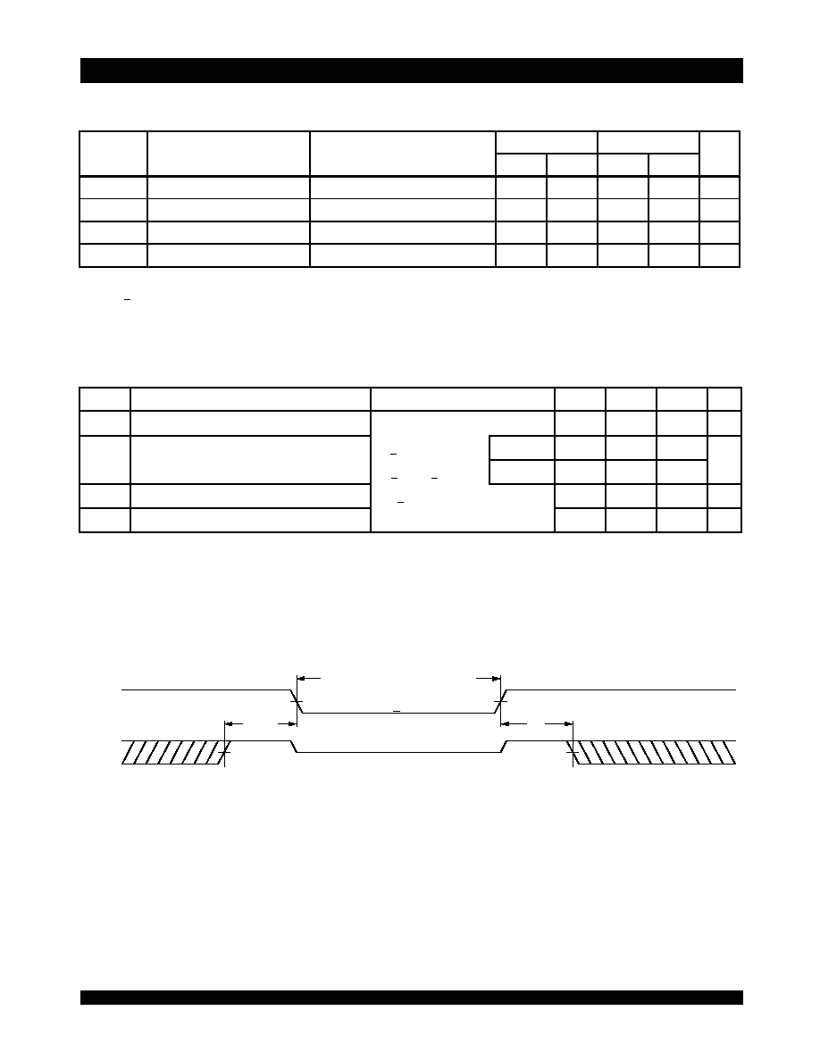
Truth Table I: Non-Contention Read/Write Control
Truth Table II: Semaphore Read/Write Control
(1)
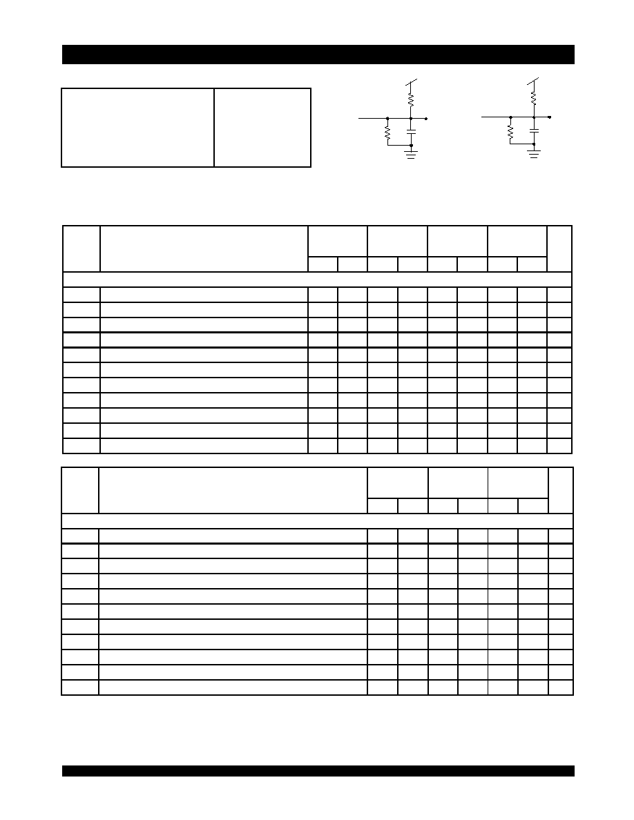
Recommended DC Operating
Conditions
Maximum Operating Temperature
and Supply Voltage
(1,2)
Absolute Maximum Ratings
(1)
Capacitance
(1)
(T
A
= +25∞C, f = 1.0mhz)
NOTE:
1. There are eight semaphore flags written to via I/O
0
and read from I/O
0 -
I/O
7
. These eight semaphores are addressed by A
0
- A
2
.
NOTE:
1. A
0L
A
13L
is not equal to A
0R
A
13R
NOTES:
1. Stresses greater than those listed under ABSOLUTE MAXIMUM RATINGS may
cause permanent damage to the device. This is a stress rating only and
functional operation of the device at these or any other conditions above those
indicated in the operational sec-tions of this specification is not implied. Exposure
to absolute maxi-mum rating conditions for extended periods may affect
reliability.
2. V
TERM
must not exceed Vcc + 10% for more than 25% of the cycle time or 10ns
maximum, and is limited to < 20mA for the period of V
TERM
< Vcc + 10%.
NOTES:
1. This is the parameter T
A
.
2. Industrial temperature: for specific speeds, packages and powers contact your
sales office.
NOTES:
1. V
IL
> -1.5V for pulse width less than 10ns.
2. V
TERM
must not exceed Vcc + 10%.
NOTES:
1. These parameters are determined by device characterization, but are not
production tested (TQFP Package Only).
2. 3dV references the interpolated capacitance when the input and output signals
switch from 0V to 3V or from 3V to 0V.
Inputs
Outputs
Mode
CE
R/W
OE
SEM
I/O
0-7
H
X
X
H
High-Z
Deselected: Power-Down
L
L
X
H
DATA
IN
Write to Memory
L
H
L
H
DATA
OUT
Read Memory
X
X
H
X
High-Z
Outputs Disabled
2739 tbl 02
Inputs
(1)
Outputs
Mode
CE
R/W
OE
SEM
I/O
0-7
H
H
L
L
DATA
OUT
Read in Semaphore Flag Data Out
H
X
L
DATA
IN
Write I/Oo into Semaphore Flag
L
X
X
L
____
Not Allowed
2739 tbl 03
Symbol
Rating
Commercial
& Industrial
Military
Unit
V
TERM
(2)
Terminal Voltage
with Respect
to GND
-0.5 to +7.0
-0.5 to +7.0
V
T
BIAS
Temperature
Under Bias
-55 to +125
-65 to +135
o
C
T
STG
Storage
Temperature
-55 to +125
-65 to +150
o
C
I
OUT
DC Output
Current
50
50
mA
2739 tbl 04
Symbol
Parameter
Conditions
(2)
Max.
Unit
C
IN
Input Capacitance
V
IN
= 3dV
9
pF
C
OUT
Output
Capacitance
V
OUT
= 3dV
10
pF
2739 tbl 05
Symbol
Parameter
Min.
Typ.
Max.
Unit
V
CC
Supply Voltage
4.5
5.0
5.5
V
GND
Ground
0
0
0
V
V
IH
Input High Voltage
2.2
____
6.0
(2)
V
V
IL
Input Low Voltage
-0.5
(1)
____
0.8
V
2739 tbl 06
Grade
Ambient
Temperature
GND
Vcc
Military
-55
O
C to+125
O
C
0V
5.0V
+
10%
Commercial
0
O
C to +70
O
C
0V
5.0V
+
10%
Industrial
40
O
C to +85
O
C
0V
5.0V
+
10%
2739 tbl 07
6.42
IDT7006S/L
High-Speed 16K x 8 Dual-Port Static RAM Military, Industrial and Commercial Temperature Ranges
5
DC Electrical Characteristics Over the 0perating
Temperature and Supply Voltage Range
(V
CC
= 5.0V ± 10%)
NOTE:
1. At Vcc < 2.0V input leakages are undefined.
Data Retention Characteristics Over All Temperature Ranges
(L Version Only)
(V
LC
= 0.2V, V
HC
= V
CC
- 0.2V)
Data Retention Waveform
NOTES:
1. T
A
= +25∞C, V
CC
= 2V, and are not production tested.
2. t
RC
= Read Cycle Time
3. This parameter is guaranteed by characterization, but is not production tested.
DATA RETENTION MODE
V
CC
CE
2739 drw 05
4.5V
t
CDR
t
R
V
IH
V
DR
V
IH
4.5V
V
DR
>
2V
Symbol
Parameter
Test Conditions
7006S
7006L
Unit
Min.
Max.
Min.
Max.
|I
LI
|
Input Leakage Current
(1)
V
CC
= 5.5V, V
IN
= 0V to V
CC
___
10
___
5
µA
|I
LO
|
Output Leakage Current
CE
= V
IH
, V
OUT
= 0V to V
CC
___
10
___
5
µA
V
OL
Output Low Voltage
I
OL
= 4mA
___
0.4
___
0.4
V
V
OH
Output High Voltage
I
OH
= -4mA
2.4
___
2.4
___
V
2739 tbl 08
Symbol
Parameter
Test Condition
Min.
Typ.
(1)
Max.
Unit
V
DR
V
CC
for Data Retention
V
CC
= 2
V
2.0
___
___
V
I
CCDR
Data Retention Current
CE
> V
HC
V
IN
> V
HC
or < V
LC
Mil. & Ind.
___
100
4000
µA
Com'l.
___
100
1500
t
CDR(3)
Chip Deselect to Data Retention Time
SEM
> V
HC
0
___
___
ns
t
R(3)
Operation Recovery Time
t
RC(2)
___
___
ns
2739 tbl 09

6
IDT7006S/L
High-Speed 16K x 8 Dual-Port Static RAM Military, Industrial and Commercial Temperature Ranges
DC Electrical Characteristics Over the Operating
Temperature and Supply Voltage Range
(1,6)
(V
CC
= 5.0V ± 10%)
NOTES:
1. 'X' in part numbers indicates power rating (S or L)
2. V
CC
= 5V, T
A
= +25∞C, and are not production tested. I
CC DC
=120ma (typ)
3. At f = f
MAX
,
address and I/O'
S
are cycling at the maximum frequency read cycle of 1/t
RC
, and using AC Test Conditions of input levels
of GND to 3V.
4. f = 0 means no address or control lines change.
5. Port "A" may be either left or right port. Port "B"is the opposite from port "A".
6. Industrial temperature: for other speeds, packages and powers contact your sales office.
7006X15
Com'l Only
7006X17
Com'l Only
7006X20
Com'l &
Military
7006X25
Com'l &
Military
Symbol
Parameter
Test Condition
Version
Typ.
(2)
Max.
Typ.
(2)
Max.
Typ.
(2)
Max.
Typ.
(2)
Max.
Unit
I
CC
Dynamic Operating
Current
(Both Ports Active)
CE
= V
IL
, Outputs Open
SEM
= V
IH
f = f
MAX
(3)
COM'L
S
L
170
160
310
260
170
160
310
260
160
150
290
240
155
145
265
220
mA
MIL &
IND
S
L
____
____
____
____
____
____
____
____
160
150
370
320
155
145
340
280
I
SB1
Standby Current
(Both Ports - TTL
Level Inputs)
CE
L
= CE
R
= V
IH
SEM
R
= SEM
L
= V
IH
f = f
MAX
(3)
COM'L
S
L
20
10
60
50
20
10
60
50
20
10
60
50
16
10
60
50
mA
MIL &
IND
S
L
____
____
____
____
____
____
____
____
20
10
90
70
16
10
80
65
I
SB2
Standby Current
(One Port - TTL
Level Inputs)
CE
"A"
= V
IL
and CE
"B"
= V
IH
(5)
Active Port Outputs Open,
f=f
MAX
(3)
SEM
R
= SEM
L
= V
IH
COM'L
S
L
105
95
190
160
105
95
190
160
95
85
180
150
90
80
170
140
mA
MIL &
IND
S
L
____
____
____
____
____
____
____
____
95
85
240
210
90
80
215
180
I
SB3
Full Standby Current (Both
Ports - All CMOS Level
Inputs)
Both Ports CE
L
and
CE
R
> V
CC
- 0.2V
V
IN
> V
CC
- 0.2V or
V
IN
< 0.2V, f = 0
(4)
SEM
R
= SEM
L
> V
CC
- 0.2V
COM'L
S
L
1.0
0.2
15
5
1.0
0.2
15
5
1.0
0.2
15
5
1.0
0.2
15
5
mA
MIL &
IND
S
L
____
____
____
____
____
____
____
____
1.0
0.2
30
10
1.0
0.2
30
10
I
SB4
Full Standby Current
(One Port - All
CMOS Level Inputs)
CE
"A"
< 0.2V and
CE
"B"
> V
CC
- 0.2V
(5)
SEM
R
= SEM
L
> V
CC
- 0.2V
V
IN
> V
CC
- 0.2V or V
IN
< 0.2V
Active Port Outputs Open
f = f
MAX
(3)
COM'L
S
L
100
90
170
140
100
90
170
140
90
80
155
130
85
75
145
120
mA
MIL &
IND
S
L
____
____
____
____
____
____
____
____
90
80
225
200
85
75
200
170
2739 tbl 10
7006X35
Com'l &
Military
7006X55
Com'l, Ind
& Military
7006X70
Military
Only
Symbol
Parameter
Test Condition
Version
Typ.
(2)
Max.
Typ.
(2)
Max.
Typ.
(2)
Max.
Unit
I
CC
Dynamic Operating
Current
(Both Ports Active)
CE
= V
IL
, Outputs Open
SEM
= V
IH
f = f
MAX
(3)
COM'L
S
L
150
140
250
210
150
140
250
210
____
____
____
____
mA
MIL &
IND
S
L
150
140
300
250
150
140
300
250
140
130
300
250
I
SB1
Standby Current
(Both Ports - TTL
Level Inputs)
CE
L
= CE
R
= V
IH
SEM
R
= SEM
L
= V
IH
f = f
MAX
(3)
COM'L
S
L
13
10
60
50
13
10
60
50
____
____
____
____
mA
MIL &
IND
S
L
13
10
80
65
13
10
80
65
10
8
80
65
I
SB2
Standby Current
(One Port - TTL
Level Inputs)
CE
"A"
= V
IL
and CE
"B"
= V
IH
(5)
Active Port Outputs Open,
f=f
MAX
(3)
SEM
R
= SEM
L
= V
IH
COM'L
S
L
85
75
155
130
85
75
155
130
____
____
____
____
mA
MIL &
IND
S
L
85
75
190
160
85
75
190
160
80
70
190
160
I
SB3
Full Standby Current
(Both Ports - All CMOS
Level Inputs)
Both Ports CE
L
and
CE
R
> V
CC
- 0.2V
V
IN
> V
CC
- 0.2V or
V
IN
< 0.2V, f = 0
(4)
SEM
R
= SEM
L
> V
CC
- 0.2V
COM'L
S
L
1.0
0.2
15
5
1.0
0.2
15
5
____
____
____
____
mA
MIL &
IND
S
L
1.0
0.2
30
10
1.0
0.2
30
10
1.0
0.2
30
10
I
SB4
Full Standby Current
(One Port - All CMOS
Level Inputs)
CE
"A"
< 0.2V and
CE
"B"
> V
CC
- 0.2V
(5)
SEM
R
= SEM
L
> V
CC
- 0.2V
V
IN
> V
CC
- 0.2V or V
IN
< 0.2V
Active Port Outputs Open
f = f
MAX
(3)
COM'L
S
L
80
70
135
110
80
70
135
110
____
____
____
____
mA
MIL &
IND
S
L
80
70
175
150
80
70
175
150
75
65
175
150
2739 tbl 11
6.42
IDT7006S/L
High-Speed 16K x 8 Dual-Port Static RAM Military, Industrial and Commercial Temperature Ranges
7
AC Test Conditions
NOTES:
1. Transition is measured ±500mV from Low or High-impedance voltage with load (Figures 1 and 2).
2. This parameter is guaranteed by device characterization, but is not production tested.
3. To access RAM, CE = V
IL
and SEM = V
IH
.
To access semaphore,
CE
= V
IH
and
SEM
= V
IL
.
4. 'X' in part numbers indicates power rating (S or L).
5. Industrial temperature: for other speeds, packages and powers contact your sales office.
Figure 2. Output Test Load
(5pF for t
LZ
, t
HZ
, t
WZ
, t
OW
)
*Including scope and jig.
Figure 1. AC Output Test Load
AC Electrical Oharacteristics Over the
Operating temperature and Supply Voltage Range
(4,5)
1250
30pF
775
DATA
OUT
BUSY
INT
5V
5V
1250
5pF*
775
DATA
OUT
2739 drw 06
,
Input Pulse Levels
Input Rise/Fall Times
Input Timing Reference Levels
Output Reference Levels
Output Load
GND to 3.0V
5ns Max.
1.5V
1.5V
Figures 1 and 2
2739 tbl 12
7006X15
Com'l Only
7006X17
Com'l Only
7006X20
Com'l & Military
7006X25
Com'l & Military
Unit
Symbol
Parameter
Min.
Max.
Min.
Max.
Min.
Max.
Min.
Max.
READ CYCLE
t
RC
Read Cycle Time
15
____
17
____
20
____
25
____
ns
t
AA
Address Access Time
____
15
____
17
____
20
____
25
ns
t
ACE
Chip Enable Access Time
(3)
____
15
____
17
____
20
____
25
ns
t
AOE
Output Enable Access Time
____
10
____
10
____
12
____
13
ns
t
OH
Output Hold from Address Change
3
____
3
____
3
____
3
____
ns
t
LZ
Output Low-Z Time
(1,2)
3
____
3
____
3
____
3
____
ns
t
HZ
Output High-Z Time
(1,2)
____
10
____
10
____
12
____
15
ns
t
PU
Chip Enable to Power Up Time
(2,5)
0
____
0
____
0
____
0
____
ns
t
PD
Chip Disable to Power Down Time
(2,5)
____
15
____
17
____
20
____
25
ns
t
SOP
Semaphore Flag Update Pulse (OE or SEM)
10
____
10
____
10
____
10
____
ns
t
SAA
Semaphore Address Access Time
____
15
____
17
____
20
____
25
ns
2739 tbl 13a
7006X35
Com'l &
Military
7006X55
Com'l, Ind
& Military
7006X70
Military
Only
Unit
Symbol
Parameter
Min.
Max.
Min.
Max.
Min.
Max.
READ CYCLE
t
RC
Read Cycle Time
35
____
55
____
70
____
ns
t
AA
Address Access Time
____
35
____
55
____
70
ns
t
ACE
Chip Enable Access Time
(3)
____
35
____
55
____
70
ns
t
AOE
Output Enable Access Time
____
20
____
30
____
35
ns
t
OH
Output Hold from Address Change
3
____
3
____
3
____
ns
t
LZ
Output Low-Z Time
(1,2)
3
____
3
____
3
____
ns
t
HZ
Output High-Z Time
(1,2)
____
15
____
25
____
30
ns
t
PU
Chip Enable to Power Up Time
(2,5)
0
____
0
____
0
____
ns
t
PD
Chip Disable to Power Down Time
(2,5)
____
35
____
50
____
50
ns
t
SOP
Semaphore Flag Update Pulse (OE or SEM)
15
____
15
____
15
____
ns
t
SAA
Semaphore Address Access Time
____
35
____
55
____
70
ns
2739 tbl 13b
8
IDT7006S/L
High-Speed 16K x 8 Dual-Port Static RAM Military, Industrial and Commercial Temperature Ranges
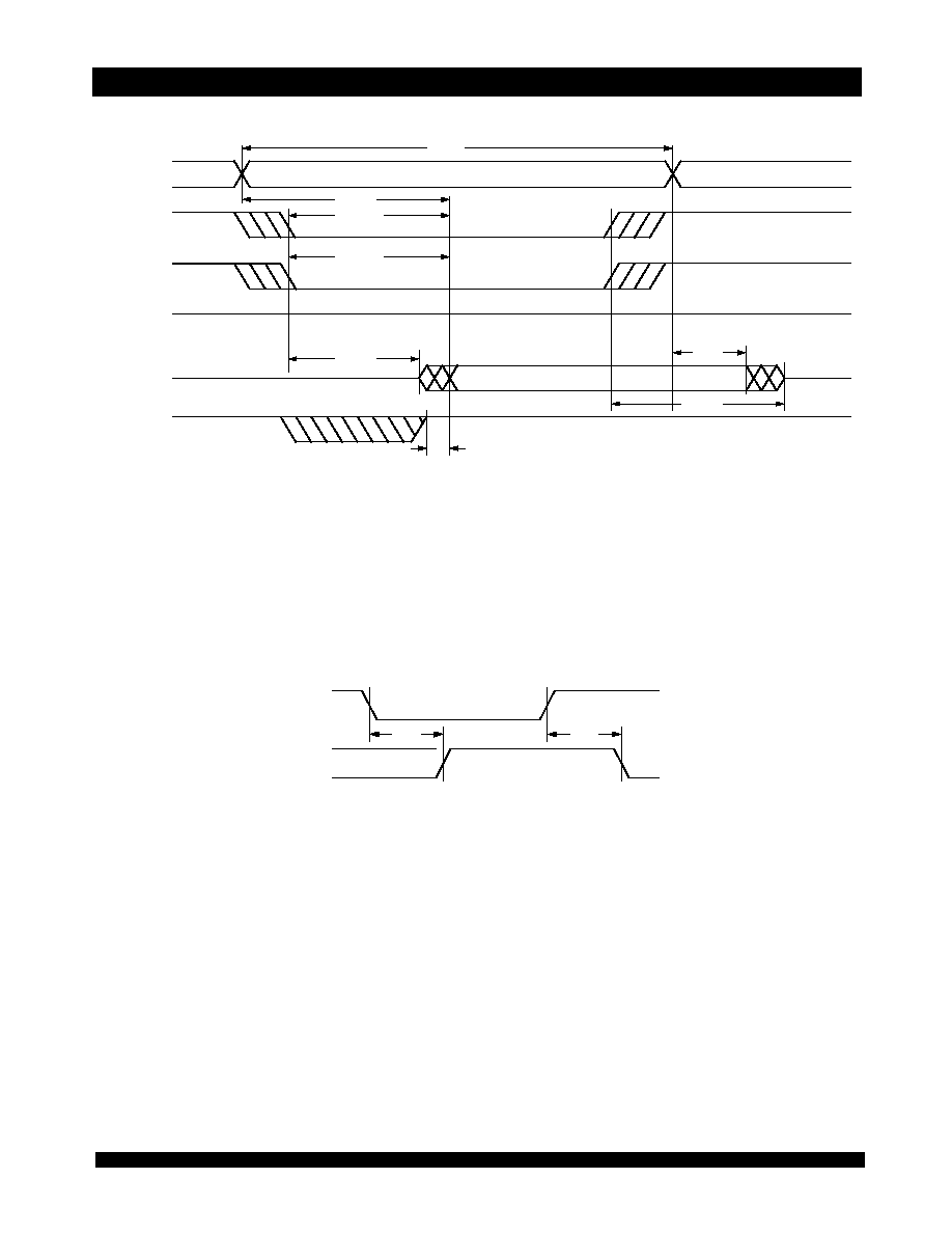
Timing of Power-Up Power-Down
Waveform of Read Cycles
(5)
NOTES:
1. Timing depends on which signal is asserted last, OE or CE.
2. Timing depends on which signal is de-asserted first CE or OE.
3. t
BDD
delay is required only in cases where the opposite port is completing a write operation to the same address location. For simultaneous read operations BUSY
has no relation to valid output data.
4. Start of valid data depends on which timing becomes effective last t
AOE
, t
ACE
, t
AA
or t
BDD
.
5. SEM = V
IH
.
t
RC
R/
W
CE
ADDR
t
AA
(4)
OE
2739 drw 07
t
ACE
(4)
t
AOE
(4)
t
LZ
(1)
t
OH
t
HZ
(2)
t
BDD
(3,4)
DATA
OUT
BUSY
OUT
VALID DATA
(4)
CE
2739 drw 08
t
PU
I
CC
I
SB
t
PD
,

6.42
IDT7006S/L
High-Speed 16K x 8 Dual-Port Static RAM Military, Industrial and Commercial Temperature Ranges
9
NOTES:
1. Transition is measured ±500mV from Low or High-impedance voltage with load (Figure 2).
2. This parameter is guaranteed by device characterization, but is not production tested but not tested.
3. To access RAM, CE = V
IL
, SEM = V
IH
. To access semaphore, CE = V
IH
and SEM = V
IL
. Either condition must be valid for the entire t
EW
time.
4. The specification for t
DH
must be met by the device supplying write data to the RAM under all operating conditions. Although t
DH
and t
OW
values will vary over voltage
and temperature, the actual t
DH
will always be smaller than the actual t
OW
.
5. 'X' in part numbers indicates power rating (S or L).
6. Industrial temperature: for other speeds, packages and powers contact your sales office.
AC Electrical Characteristics Over the
Operating Temperature and Supply Voltage
(5,6)
Symbol
Parameter
7006X15
Com'l Only
7006X17
Com'l Only
7006X20
Com'l &
Military
7006X25
Com'l &
Military
Unit
Min.
Max.
Min.
Max.
Min.
Max.
Min.
Max.
WRITE CYCLE
t
WC
Write Cycle Time
15
____
17
____
20
____
25
____
ns
t
EW
Chip Enable to End-of-Write
(3)
12
____
12
____
15
____
20
____
ns
t
AW
Address Valid to End-of-Write
12
____
12
____
15
____
20
____
ns
t
AS
Address Set-up Time
(3)
0
____
0
____
0
____
0
____
ns
t
WP
Write Pulse Width
12
____
12
____
15
____
20
____
ns
t
WR
Write Recovery Time
0
____
0
____
0
____
0
____
ns
t
DW
Data Valid to End-of-Write
10
____
10
____
15
____
15
____
ns
t
HZ
Output High-Z Time
(1,2)
____
10
____
10
____
12
____
15
ns
t
DH
Data Hold Time
(4)
0
____
0
____
0
____
0
____
ns
t
WZ
Write Enable to Output in High-Z
(1,2)
____
____
____
____
____
12
____
15
ns
t
OW
Output Active from End-of-Write
(1,2,4)
0
____
0
____
0
____
0
____
ns
t
SWRD
SEM
Flag Write to Read Time
5
____
5
____
5
____
5
____
ns
t
SPS
SEM
Flag Contention Window
5
____
5
____
5
____
5
____
ns
2739 tbl 14a
Symbol
Parameter
7006X35
Com'l & Military
7006X55
Com'l, Ind
& Military
7006X70
Military
Only
Unit
Min.
Max.
Min.
Max.
Min.
Max.
WRITE CYCLE
t
WC
Write Cycle Time
35
____
55
____
70
____
ns
t
EW
Chip Enable to End-of-Write
(3)
30
____
45
____
50
____
ns
t
AW
Address Valid to End-of-Write
30
____
45
____
50
____
ns
t
AS
Address Set-up Time
(3)
0
____
0
____
0
____
ns
t
WP
Write Pulse Width
25
____
40
____
50
____
ns
t
WR
Write Recovery Time
0
____
0
____
0
____
ns
t
DW
Data Valid to End-of-Write
15
____
30
____
40
____
ns
t
HZ
Output High-Z Time
(1,2)
____
15
____
25
____
30
ns
t
DH
Data Hold Time
(4)
0
____
0
____
0
____
ns
t
WZ
Write Enable to Output in High-Z
(1,2)
____
15
____
25
____
30
ns
t
OW
Output Active from End-of-Write
(1,2,4)
0
____
0
____
0
____
ns
t
SWRD
SEM
Flag Write to Read Time
5
____
5
____
5
____
ns
t
SPS
SEM
Flag Contention Window
5
____
5
____
5
____
ns
2739 tbl 14b
10
IDT7006S/L
High-Speed 16K x 8 Dual-Port Static RAM Military, Industrial and Commercial Temperature Ranges
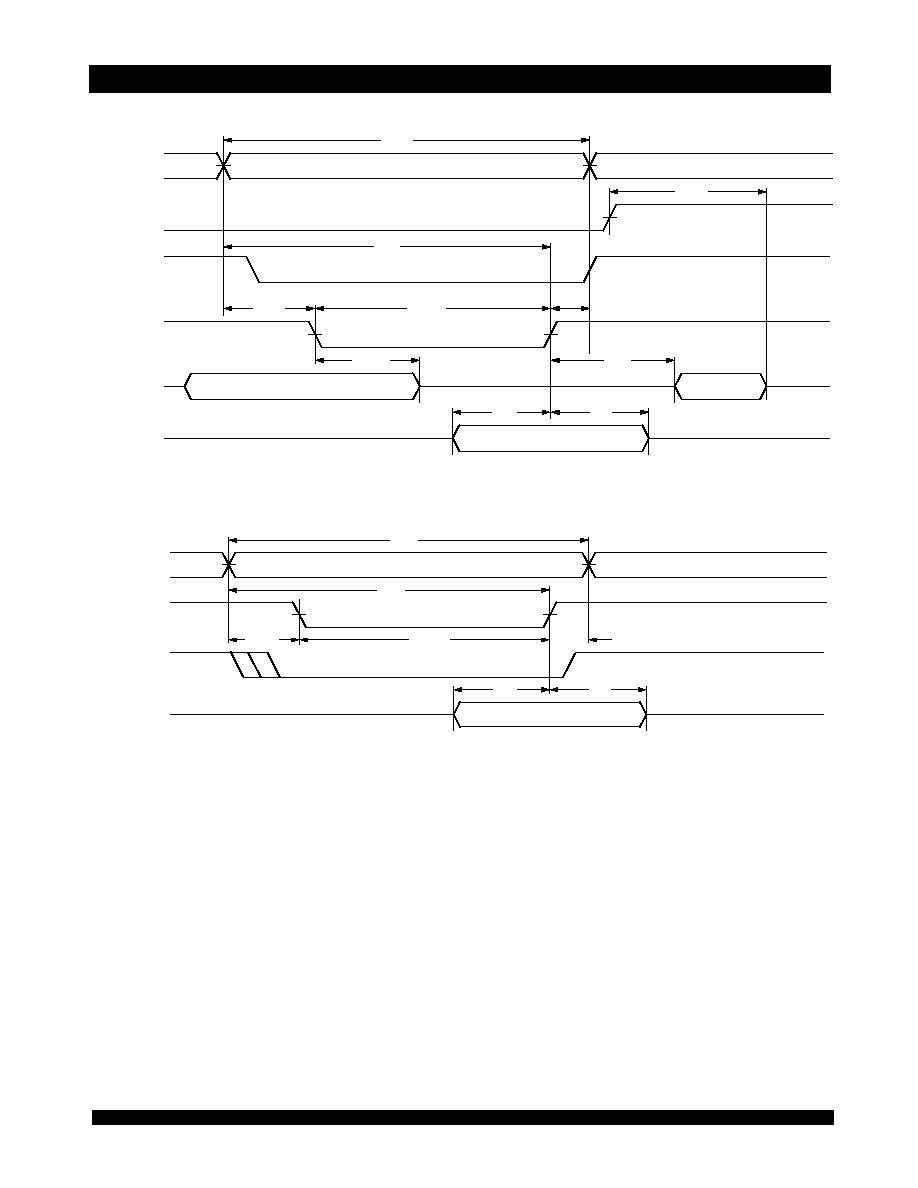
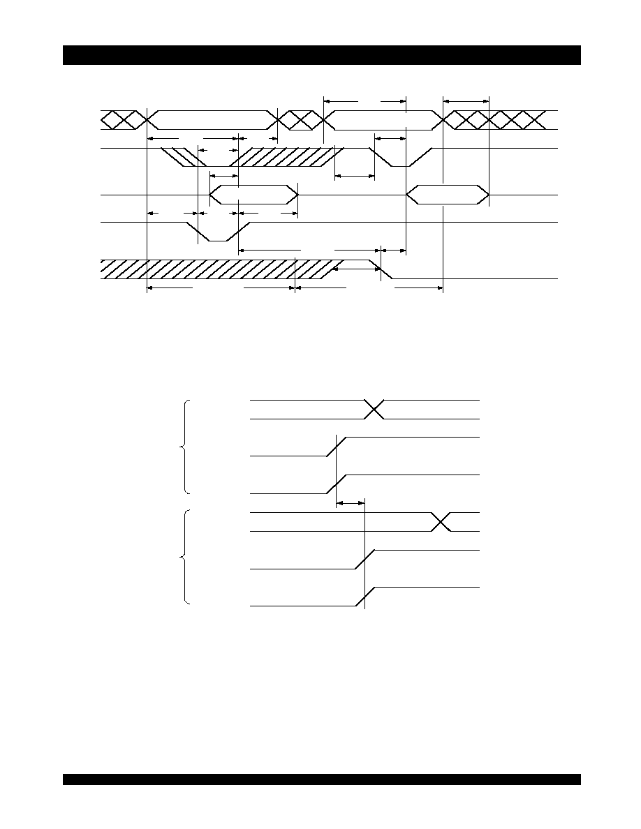
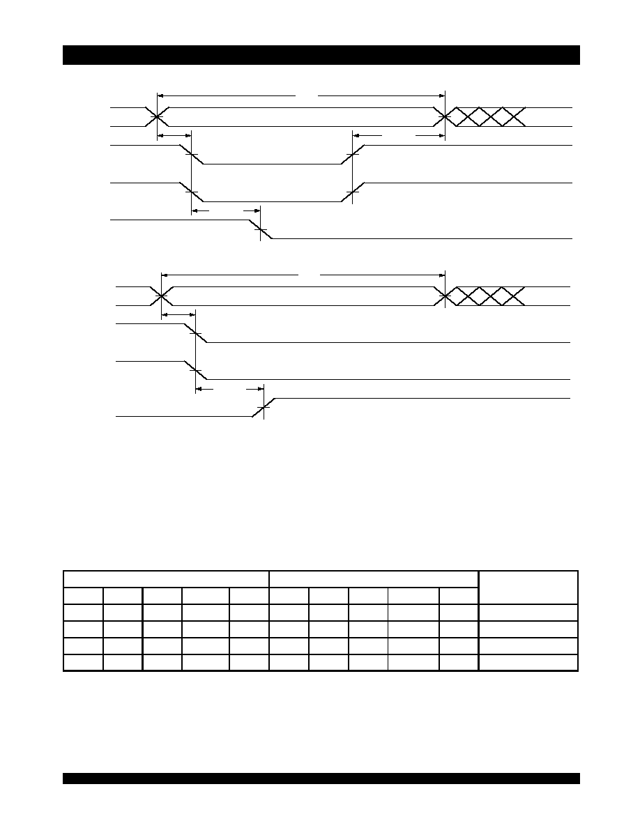
Timing Waveform of Write Cycle No. 1, R/W Controlled Timing
(1,5,8)
Timing Waveform of Write Cycle No. 2, CE Controlled Timing
(1,5)
NOTES:
1. R/W or CE must be HIGH during all address transitions.
2. A write occurs during the overlap (t
EW
or t
WP
) of a LOW CE and a LOW R/W for memory array writing cycle.
3. t
WR
is measured from the earlier of CE or R/W (or SEM or R/W) going HIGH to the end of write cycle.
4. During this period, the I/O pins are in the output state and input signals must not be applied.
5. If the CE or SEM LOW transition occurs simultaneously with or after the R/W low transition, the outputs remain in the High-impedance state.
6. Timing depends on which enable signal is asserted last, CE or R/W.
7. This parameter is guaranteed by device characterization, but is not production tested. Transition is measured by ±500mV from steady state with the Output Test
Load (Figure 2).
8. If OE is LOW during R/W controlled write cycle, the write pulse width must be the larger of t
WP
or (t
WZ
+ t
DW
) to allow the I/O drivers to turn off and data to be placed
on the bus for the required t
DW
. If OE is HIGH during an R/W controlled write cycle, this requirement does not apply and the write pulse can be as short as the specified
t
WP
.
9. To access RAM, CE = V
IL
and
SEM
= V
IH
.
To access semaphore CE = V
IH
and
SEM
= V
IL
.
t
EW
must be met for either condition.
R/
W
t
WC
t
HZ
(7)
t
AW
t
WR
(3)
t
AS
(6)
t
WP
(2)
DATA
OUT
t
WZ
(7)
t
DW
t
DH
t
OW
OE
ADDRESS
DATA
IN
(4)
(4)
2739 drw 09
CE
or
SEM
(9)
2739 drw 10
t
WC
t
AS
(6)
t
WR
(3)
t
DW
t
DH
ADDRESS
DATA
IN
CE
or
SEM
(9)
R/
W
t
AW
t
EW
(2)
6.42
IDT7006S/L
High-Speed 16K x 8 Dual-Port Static RAM Military, Industrial and Commercial Temperature Ranges
11
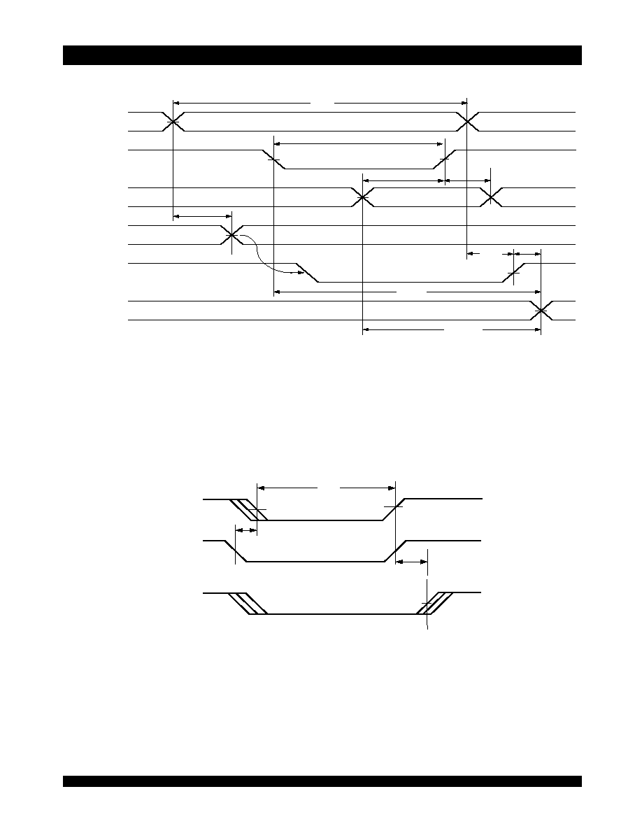
Timing Waveform of Semaphore Read after Write Timing, Either Side
(1)
NOTE:
1. CE = V
IH
for the duration of the above timing (both write and read cycle).
NOTES:
1. D
OR
= D
OL
= V
IL
, CE
R
= CE
L
= V
IH
, Semaphore Flag is released from both sides (reads as ones from both sides) at cycle start.
2. All timing is the same for left and right ports. Port A may be either left or right port. Port B is the opposite from port A.
3. This parameter is measured from R/W
"A"
or SEM
"A"
going HIGH to R/W
"B"
or SEM
"B"
going HIGH.
4. If t
SPS
is not satisfied, the semaphore will fall positively to one side or the other, but there is no guarantee which side will obtain the flag.
Timing Waveform of Semaphore Write Contention
(1,3,4)
SEM
2739 drw 11
t
AW
t
EW
t
SOP
DATA
0
VALID ADDRESS
t
SAA
R/
W
t
WR
t
OH
t
ACE
VALID ADDRESS
DATA
IN
VALID
t
DW
t
WP
t
DH
t
AS
t
SWRD
t
AOE
t
SOP
Read Cycle
Write Cycle
A
0
-A
2
OE
DATA
OUT
VALID
SEM
"A"
2739 drw 12
t
SPS
MATCH
R/
W
"A"
MATCH
A
0"A"
-A
2"A"
SIDE
"A"
(2)
SEM
"B"
R/
W
"B"
A
0"B"
-A
2"B"
SIDE
"B"
(2)
12
IDT7006S/L
High-Speed 16K x 8 Dual-Port Static RAM Military, Industrial and Commercial Temperature Ranges
NOTES:
1. Port-to-port delay through RAM cells from writing port to reading port, refer to "Timing Waveform of Write with Port-to-Port Read and BUSY".
2. To ensure that the earlier of the two ports wins.
3. t
BDD
is a calculated parameter and is the greater of 0, t
WDD
t
WP
(actual) or t
DDD
t
DW
(actual).
4. To ensure that the write cycle is inhibited with port "B" during contention on port "A".
5. To ensure that a write cycle is completed on port "B" after contention with port "A".
6. 'X' is part numbers indicates power rating (S or L).
7. Industrial temperature: for other speeds, packages and powers contact your sales office.
AC Electrical Characteristics Over the
Operating Temperature and Supply Voltage Range
(6,7)
7006X15
Com'l Only
7006X17
Com'l Only
7006X20
Com'l &
Military
7006X25
Com'l &
Military
Symbol
Parameter
Min.
Max.
Min.
Max.
Min.
Max.
Min.
Max.
Unit
BUSY
TIMING (M/S=V
IH
)
t
BAA
BUSY
Access Time from Address Match
____
15
____
17
____
20
____
20
ns
t
BDA
BUSY
Disable Time from Address Not Matched
____
15
____
17
____
20
____
20
ns
t
BAC
BUSY
Access Time from Chip Enable Low
____
15
____
17
____
20
____
20
ns
t
BDC
BUSY
Access Time from Chip Enable High
____
15
____
17
____
17
____
17
ns
J
APS
Arbitration Priority Set-up Time
(2)
5
____
5
____
5
____
5
____
ns
t
BDD
BUSY
Disable to Valid Data
(3)
____
18
____
18
____
30
____
30
ns
t
WH
Write Hold After BUSY
(5)
12
____
13
____
15
____
17
____
ns
BUSY
TIMING (M/S=V
IL
)
t
WB
BUSY
Input to Write
(4)
0
____
0
____
0
____
0
____
ns
t
WH
Write Hold After BUSY
(5)
12
____
13
____
15
____
17
____
ns
PORT-TO-PORT DELAY TIMING
t
WDD
Write Pulse to Data Delay
(1)
____
30
____
30
____
45
____
50
ns
t
DDD
Write Data Valid to Read Data Delay
(1)
____
25
____
25
____
35
____
35
ns
2739 tbl 15a
7006X35 Com'l
& Military
7006X55
Com'l, Ind
& Military
7006X70
Military
Only
Symbol
Parameter
Min.
Max.
Min.
Max.
Min.
Max.
Unit
BUSY
TIMING (M/S=V
IH
)
t
BAA
BUSY
Access Time from Address Match
____
20
____
45
____
45
ns
t
BDA
BUSY
Disable Time from Address Not Matched
____
20
____
40
____
40
ns
t
BAC
BUSY
Access Time from Chip Enable Low
____
20
____
40
____
40
ns
t
BDC
BUSY
Access Time from Chip Enable High
____
20
____
35
____
35
ns
t
APS
Arbitration Priority Set-up Time
(2)
5
____
5
____
5
____
ns
t
BDD
BUSY
Disable to Valid Data
(3)
____
35
____
40
____
45
ns
t
WH
Write Hold After BUSY
(5)
25
____
25
____
25
____
ns
BUSY
TIMING (M/S=V
IL
)
t
WB
BUSY
Input to Write
(4)
0
____
0
____
0
____
ns
t
WH
Write Hold After BUSY
(5)
25
____
25
____
25
____
ns
PORT-TO-PORT DELAY TIMING
t
WDD
Write Pulse to Data Delay
(1)
____
60
____
80
____
95
ns
t
DDD
Write Data Valid to Read Data Delay
(1)
____
45
____
65
____
80
ns
2739 tbl 15b
6.42
IDT7006S/L
High-Speed 16K x 8 Dual-Port Static RAM Military, Industrial and Commercial Temperature Ranges
13
Timing Waveform of Write with Port-to-Port Read and BUSY
(2,5)
(M/S = V
IH
)
(4)
Timing Waveform of Write with BUSY
NOTES:
1. t
WH
must be met for both BUSY input (slave) and output (master).
2. BUSY is asserted on Port "B", blocking R/W
"B"
, until BUSY
"B"
goes HIGH.
3. t
WB
is only for the 'Slave' Version
.
2739 drw 13
t
DW
t
APS
(1)
ADDR
"A"
t
WC
DATA
OUT "B"
MATCH
t
WP
R/
W
"A"
DATA
IN "A"
ADDR
"B"
t
DH
VALID
MATCH
BUSY
"B"
t
BDA
VALID
t
BDD
t
DDD
(3)
t
WDD
2739 drw 14
R/
W
"A"
BUSY
"B"
t
WP
t
WB
(3)
R/
W
"B"
t
WH
(1)
(2)
NOTES:
1. To ensure that the earlier of the two ports wins. t
APS
is ignored for M/S = V
IL
(SLAVE).
2. CE
L
= CE
R
= V
IL
3. OE = V
IL
for the reading port.
4. If M/S = V
IL
(slave) then BUSY is input (BUSY
"A"
= V
IH
)
and BUSY
"B"
= "don't care", for this example.
5. All timing is the same for left and right port. Port "A' may be either left or right port. Port "B" is the port opposite from Port "A".
14
IDT7006S/L
High-Speed 16K x 8 Dual-Port Static RAM Military, Industrial and Commercial Temperature Ranges
Waveform of BUSY Arbitration Controlled by CE Timing
(1)
(M/S = V
IH
)
Waveform of BUSY Arbitration Cycle Controlled by Address Match
Timing
(1)
(M/S = V
IH
)
NOTES:
1. All timing is the same for left and right ports. Port A may be either the left or right port. Port B is the port opposite from port A.
2. If t
APS
is not satisfied, the BUSY signal will be asserted on one side or another but there is no guarantee on which side BUSY will be asserted.
AC Electrical Characteristics Over the
Operating Temperature and Supply Voltage Range
(1,2)
NOTES:
1. 'X' in part numbers indicates power rating (S or L).
2. Industrial temperature: for other speeds, packages and powers contact your sales office.
2739 drw 15
ADDR
"A"
and
"B"
ADDRESSES MATCH
CE
"A"
CE
"B"
BUSY
"B"
t
APS
(2)
t
BAC
t
BDC
2739 drw 16
ADDR
"A"
ADDRESS "N"
ADDR
"B"
BUSY
"B"
t
APS
(2)
t
BAA
t
BDA
MATCHING ADDRESS "N"
7006X15
Com'l Only
7006X17
Com'l Only
7006X20
Com'l &
Military
7006X25
Com'l &
Military
Symbol
Parameter
Min.
Max.
Min.
Max.
Min.
Max.
Min.
Max.
Unit
INTERRUPT TIMING
t
AS
Address Set-up Time
0
____
0
____
0
____
0
____
ns
t
WR
Write Recovery Time
0
____
0
____
0
____
0
____
ns
t
INS
Interrupt Set Time
____
15
____
15
____
20
____
20
ns
t
INR
Interrupt Reset Time
____
15
____
15
____
20
____
20
ns
2739 tbl 16a
7006X35
Com'l &
Military
7006X55
Com'l, Ind
& Military
7006X70
Military Only
Symbol
Parameter
Min.
Max.
Min.
Max.
Min.
Max.
Unit
INTERRUPT TIMING
t
AS
Address Set-up Time
0
____
0
____
0
____
ns
t
WR
Write Recovery Time
0
____
0
____
0
____
ns
t
INS
Interrupt Set Time
____
25
____
40
____
50
ns
t
INR
Interrupt Reset Time
____
25
____
40
____
50
ns
2739 tbl 16b
6.42
IDT7006S/L
High-Speed 16K x 8 Dual-Port Static RAM Military, Industrial and Commercial Temperature Ranges
15
Waveform of Interrupt Timing
(1)
Truth Tables
Truth Table III Interrupt Flag
(1,4)
NOTES:
1. All timing is the same for left and right ports. Port A may be either the left or right port. Port B is the port opposite from port A.
2. See Interrupt Truth Table III.
3. Timing depends on which enable signal (CE or R/W) is asserted last.
4. Timing depends on which enable signal (CE or R/W) is de-asserted first.
NOTES:
1. Assumes BUSY
L
= BUSY
R
= V
IH
.
2. If BUSY
L
= V
IL
, then no change.
3. If BUSY
R
= V
IL
, then no change.
4. INT
R and
INT
L
must be initialized at power-up.
2739 drw 17
ADDR
"A"
INTERRUPT SET ADDRESS
(2)
CE
"A"
R/
W
"A"
t
AS
(3)
t
WC
t
WR
(4)
t
INS
(3)
INT
"B"
2739 drw 18
ADDR
"B"
INTERRUPT CLEAR ADDRESS
(2)
CE
"B"
OE
"B"
t
AS
(3)
t
RC
t
INR
(3)
INT
"B"
Left Port
Right Port
Function
R/W
L
CE
L
OE
L
A
13L
-A
0L
INT
L
R/W
R
CE
R
OE
R
A
13R
-A
0R
INT
R
L
L
X
3FFF
X
X
X
X
X
L
(2)
Set Right INT
R
Flag
X
X
X
X
X
X
L
L
3FFF
H
(3)
Reset Right INT
R
Flag
X
X
X
X
L
(3)
L
L
X
3FFE
X
Set Left INT
L
Flag
X
L
L
3FFE
H
(2)
X
X
X
X
X
Reset Left INT
L
Flag
2739 tbl 17

16
IDT7006S/L
High-Speed 16K x 8 Dual-Port Static RAM Military, Industrial and Commercial Temperature Ranges
Truth Table IV Address BUSY Arbitration
NOTES:
1. Pins BUSY
L
and BUSY
R
are both outputs when the part is configured as a master. Both are inputs when configured as a slave. BUSY
X
outputs on the IDT7006 are
push pull, not open drain outputs. On slaves the BUSY
X
input internally inhibits writes.
2. "L" if the inputs to the opposite port were stable prior to the address and enable inputs of this port. "H" if the inputs to the opposite port became stable after the address
and enable inputs of this port. If t
APS
is not met, either BUSY
L
or BUSY
R
= LOW will result. BUSY
L
and BUSY
R
outputs cannot be low simultaneously.
3. Writes to the left port are internally ignored when BUSY
L
outputs are driving low regardless of actual logic level on the pin. Writes to the right port are internally ignored
when BUSY
R
outputs are driving LOW regardless of actual logic level on the pin.
Truth Table V Example of Semaphore Procurement Sequence
(1,2,3)
NOTES:
1. This table denotes a sequence of events for only one of the eight semaphores on the IDT7006.
2. There are eight semaphore flags written to via I/O
0
and read from all I/O's. These eight semaphores are addressed by A
0
- A
2
.
3. CE = V
IH
, SEM = V
IL
to access the semaphores. Refer to the Semaphore Read/Write Control Truth Table.
The left port clears the interrupt by reading address location 3FFE access
when CE
R
= OE
R
= V
IL,
R/W is a "don't care". Likewise, the right port
interrupt flag (INT
R
) is asserted when the left port writes to memory location
3FFF (HEX) and to clear the interrupt flag (INT
R
), the right port must read
the memory location 3FFF. The message (8 bits) at 3FFE or 3FFF is user-
defined, since it is an addressable SRAM location. If the interrupt function
is not used, address locations 3FFE and 3FFF are not used as mail boxes,
but as part of the random access memory. Refer to Truth Table III for the
interrupt operation.
Busy Logic
Busy Logic provides a hardware indication that both ports of the RAM
Functional Description
The IDT7006 provides two ports with separate control, address and
I/O pins that permit independent access for reads or writes to any location
in memory. The IDT7006 has an automatic power down feature controlled
by CE. The CE controls on-chip power down circuitry that permits the
respective port to go into a standby mode when not selected (CE HIGH).
When a port is enabled, access to the entire memory array is permitted.
Interrupts
If the user chooses the interrupt function, a memory location (mail box
or message center) is assigned to each port. The left port interrupt flag
(INT
L
) is asserted when the right port writes to memory location 3FFE
(HEX) where a write is defined as CE = R/W = V
IL
per the Truth Table
.
Inputs
Outputs
Function
CE
L
CE
R
A
OL
-A
13L
A
OR
-A
13R
BUSY
L
(1)
BUSY
R
(1)
X
X
NO MATCH
H
H
Normal
H
X
MATCH
H
H
Normal
X
H
MATCH
H
H
Normal
L
L
MATCH
(2)
(2)
Write Inhibit
(3)
2739 tbl 18
Functions
D
0
- D
7
Left
D
0
- D
7
Right
Status
No Action
1
1
Semaphore free
Left Port Writes "0" to Semaphore
0
1
Left port has semaphore token
Right Port Writes "0" to Semaphore
0
1
No change. Right side has no write access to semaphore
Left Port Writes "1" to Semaphore
1
0
Right port obtains semaphore token
Left Port Writes "0" to Semaphore
1
0
No change. Left port has no write access to semaphore
Right Port Writes "1" to Semaphore
0
1
Left port obtains semaphore token
Left Port Writes "1" to Semaphore
1
1
Semaphore free
Right Port Writes "0" to Semaphore
1
0
Right port has semaphore token
Right Port Writes "1" to Semaphore
1
1
Semaphore free
Left Port Writes "0" to Semaphore
0
1
Left port has semaphore token
Left Port Writes "1" to Semaphore
1
1
Semaphore free
2739 tbl 19
6.42
IDT7006S/L
High-Speed 16K x 8 Dual-Port Static RAM Military, Industrial and Commercial Temperature Ranges
17
Figure 3. Busy and chip enable routing for both width and depth expansion with IDT7006 RAMs.
have accessed the same location at the same time. It also allows one of the
two accesses to proceed and signals the other side that the RAM is busy.
The BUSY pin can then be used to stall the access until the operation on
the other side is completed. If a write operation has been attempted from
the side that receives a BUSY indication, the write signal is gated internally
to prevent the write from proceeding.
The use of BUSY logic is not required or desirable for all applications.
In some cases it may be useful to logically OR the BUSY outputs together
and use any BUSY indication as an interrupt source to flag the event of
an illegal or illogical operation. If the write inhibit function of BUSY logic is
not desirable, the BUSY logic can be disabled by placing the part in slave
mode with the M/S pin. Once in slave mode the BUSY pin operates solely
as a write inhibit input pin. Normal operation can be programmed by tying
the BUSY pins HIGH. If desired, unintended write operations can be
prevented to a port by tying the BUSY pin for that port LOW.
The BUSY outputs on the IDT 7006 RAM in master mode, are push-
pull type outputs and do not require pull up resistors to operate. If these
RAMs are being expanded in depth, then the BUSY indication for the
resulting array requires the use of an external AND gate.
Width Expansion with Busy Logic
Master/Slave Arrays
When expanding an IDT7006 RAM array in width while using BUSY
logic, one master part is used to decide which side of the RAMs array will
receive a BUSY indication, and to output that indication. Any number of
slaves to be addressed in the same address range as the master, use the
BUSY
signal as a write inhibit signal. Thus on the IDT7006 RAM the BUSY
pin is an output if the part is used as a master (M/S pin = V
IH
), and the BUSY
pin is an input if the part used as a slave (M/S pin = V
IL
) as shown in
Figure 3.
If two or more master parts were used when expanding in width, a split
decision could result with one master indicating BUSY on one side of the
array and another master indicating BUSY on one other side of the array.
This would inhibit the write operations from one port for part of a word and
inhibit the write operations from the other port for the other part of the word.
The BUSY arbitration, on a master, is based on the chip enable and
address signals only. It ignores whether an access is a read or write. In
a master/slave array, both address and chip enable must be valid long
enough for a BUSY flag to be output from the master before the actual write
pulse can be initiated with the R/W signal. Failure to observe this timing can
result in a glitched internal write inhibit signal and corrupted data in the
slave.
SEMAPHORES
The IDT7006 is an extremely fast Dual-Port 16K x 8 CMOS Static RAM
with an additional 8 address locations dedicated to binary semaphore flags.
These flags allow either processor on the left or right side of the Dual-Port
RAM to claim a privilege over the other processor for functions defined by
the system designers software. As an example, the semaphore can be
used by one processor to inhibit the other from accessing a portion of the
Dual-Port RAM or any other shared resource.
The Dual-Port RAM features a fast access time, and both ports are
completely independent of each other. This means that the activity on the
left port in no way slows the access time of the right port. Both ports are
identical in function to standard CMOS Static RAM and can be read from,
or written to, at the same time with the only possible conflict arising from the
simultaneous writing of, or a simultaneous READ/WRITE of, a non-
semaphore location. Semaphores are protected against such ambiguous
situations and may be used by the system program to avoid any conflicts
in the non-semaphore portion of the Dual-Port RAM. These devices have
an automatic power-down feature controlled by CE, the Dual-Port RAM
enable, and SEM, the semaphore enable. The CE and SEM pins control
on-chip power down circuitry that permits the respective port to go into
standby mode when not selected. This is the condition which is shown in
Truth Table I where CE and SEM are both HIGH.
Systems which can best use the IDT7006 contain multiple processors
or controllers and are typically very high-speed systems which are
software controlled or software intensive. These systems can benefit from
a performance increase offered by the IDT7006s hardware semaphores,
which provide a lockout mechanism without requiring complex program-
ming.
Software handshaking between processors offers the maximum in
system flexibility by permitting shared resources to be allocated in varying
configurations. The IDT7006 does not use its semaphore flags to control
2739 drw 19
MASTER
Dual Port
RAM
BUSY
(L)
BUSY
(R)
CE
MASTER
Dual Port
RAM
BUSY
(L)
BUSY
(R)
CE
SLAVE
Dual Port
RAM
BUSY
(L)
BUSY
(R)
CE
SLAVE
Dual Port
RAM
BUSY
(L)
BUSY
(R)
CE
BUSY
(L)
BUSY
(R)

18
IDT7006S/L
High-Speed 16K x 8 Dual-Port Static RAM Military, Industrial and Commercial Temperature Ranges
any resources through hardware, thus allowing the system designer total
flexibility in system architecture.
An advantage of using semaphores rather than the more common
methods of hardware arbitration is that wait states are never incurred in
either processor. This can prove to be a major advantage in very high-
speed systems.
How the Semaphore Flags Work
The semaphore logic is a set of eight latches which are independent
of the Dual-Port RAM. These latches can be used to pass a flag, or token,
from one port to the other to indicate that a shared resource is in use. The
semaphores provide a hardware assist for a use assignment method
called Token Passing Allocation. In this method, the state of a semaphore
latch is used as a token indicating that shared resource is in use. If the left
processor wants to use this resource, it requests the token by setting the
latch. This pro-cessor then verifies its success in setting the latch by reading
it. If it was successful, it proceeds to assume control over the shared
resource. If it was not successful in setting the latch, it determines that the
right side processor has set the latch first, has the token and is using the
shared resource. The left processor can then either repeatedly request
that semaphores status or remove its request for that semaphore to perform
another task and occasionally attempt again to gain control of the token via
the set and test sequence. Once the right side has relinquished the token,
the left side should succeed in gaining control.
The semaphore flags are active LOW. A token is requested by writing
a zero into a semaphore latch and is released when the same side writes
a one to that latch.
The eight semaphore flags reside within the IDT7006 in a separate
memory space from the Dual-Port RAM. This address space is accessed
by placing a LOW input on the SEM pin (which acts as a chip select for the
semaphore flags) and using the other control pins (Address, OE, and
R/W) as they would be used in accessing a standard Static RAM. Each
of the flags has a unique address which can be accessed by either side
through address pins A
0
A
2
. When accessing the semaphores, none
of the other address pins has any effect.
When writing to a semaphore, only data pin D
0
is used. If a LOW level
is written into an unused semaphore location, that flag will be set to a zero
on that side and a one on the other side (see Truth Table V). That
semaphore can now only be modified by the side showing the zero. When
a one is written into the same location from the same side, the flag will be
set to a one for both sides (unless a semaphore request from the other side
is pending) and then can be written to by both sides. The fact that the side
which is able to write a zero into a semaphore subsequently locks out writes
from the other side is what makes semaphore flags useful in interprocessor
communications. (A thorough discussion on the use of this feature follows
shortly.) A zero written into the same location from the other side will be
stored in the semaphore request latch for that side until the semaphore is
freed by the first side.
When a semaphore flag is read, its value is spread into all data bits so
that a flag that is a one reads as a one in all data bits and a flag containing
a zero reads as all zeros. The read value is latched into one sides output
register when that side's semaphore select (SEM) and output enable (OE)
signals go active. This serves to disallow the semaphore from changing
state in the middle of a read cycle due to a write cycle from the other side.
Because of this latch, a repeated read of a semaphore in a test loop must
cause either signal (SEM or OE) to go inactive or the output will never
change.
A sequence WRITE/READ must be used by the semaphore in order
to guarantee that no system level contention will occur. A processor
requests access to shared resources by attempting to write a zero into a
semaphore location. If the semaphore is already in use, the semaphore
request latch will contain a zero, yet the semaphore flag will appear as one,
a fact which the processor will verify by the subsequent read (see Truth
Table V). As an example, assume a processor writes a zero to the left port
at a free semaphore location. On a subsequent read, the processor will
verify that it has written successfully to that location and will assume control
over the resource in question. Meanwhile, if a processor on the right side
attempts to write a zero to the same semaphore flag it will fail, as will be
verified by the fact that a one will be read from that semaphore on the right
side during subsequent read. Had a sequence of READ/WRITE been
used instead, system contention problems could have occurred during the
gap between the read and write cycles.
It is important to note that a failed semaphore request must be followed
by either repeated reads or by writing a one into the same location. The
reason for this is easily understood by looking at the simple logic diagram
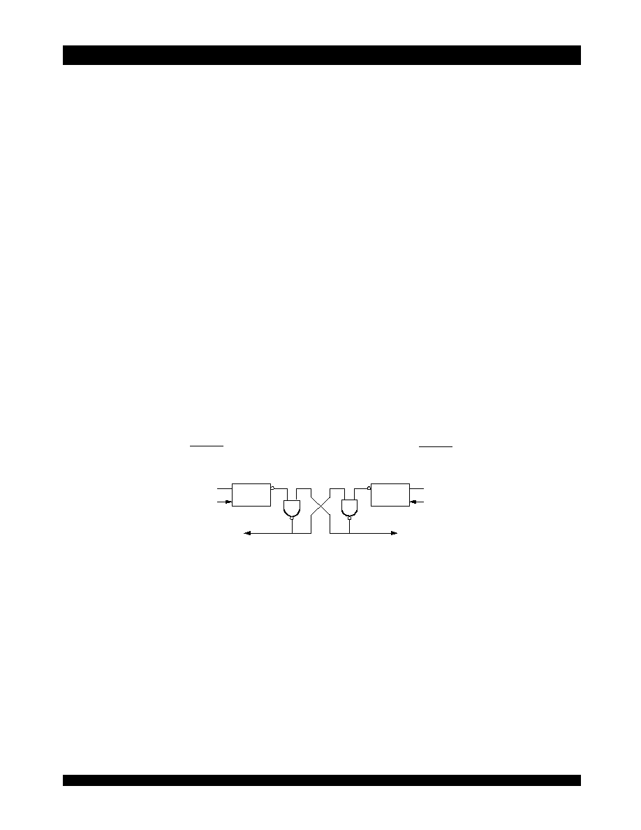
of the semaphore flag in Figure 4. Two semaphore request latches feed
into a semaphore flag. Whichever latch is first to present a zero to the
semaphore flag will force its side of the semaphore flag LOW and the other
side HIGH. This condition will continue until a one is written to the same
semaphore request latch. Should the other sides semaphore request latch
have been written to a zero in the meantime, the semaphore flag will flip
over to the other side as soon as a one is written into the first sides request
latch. The second sides flag will now stay LOW until its semaphore request
latch is written to a one. From this it is easy to understand that, if a semaphore
is requested and the processor which requested it no longer needs the
resource, the entire system can hang up until a one is written into that
semaphore request latch.
The critical case of semaphore timing is when both sides request a
single token by attempting to write a zero into it at the same time. The
semaphore logic is specially designed to resolve this problem. If simulta-
neous requests are made, the logic guarantees that only one side receives
the token. If one side is earlier than the other in making the request, the first
side to make the request will receive the token. If both requests arrive at
the same time, the assignment will be arbitrarily made to one port or the
other.
One caution that should be noted when using semaphores is that
semaphores alone do not guarantee that access to a resource is secure.
As with any powerful programming technique, if semaphores are misused
or misinterpreted, a software error can easily happen.
Initialization of the semaphores is not automatic and must be handled
via the initialization program at power-up. Since any semaphore request
flag which contains a zero must be reset to a one, all semaphores on both
sides should have a one written into them at initialization from both sides
to assure that they will be free when needed.
Using SemaphoresSome Examples
Perhaps the simplest application of semaphores is their application as
resource markers for the IDT7006s Dual-Port RAM. Say the 16K x 8 RAM
was to be divided into two 8K x 8 blocks which were to be dedicated at any
one time to servicing either the left or right port. Semaphore 0 could be used
6.42
IDT7006S/L
High-Speed 16K x 8 Dual-Port Static RAM Military, Industrial and Commercial Temperature Ranges
19
to indicate the side which would control the lower section of memory, and
Semaphore 1 could be defined as the indicator for the upper section of
memory.
To take a resource, in this example the lower 8K of Dual-Port RAM,
the processor on the left port could write and then read a zero in to
Semaphore 0. If this task were successfully completed (a zero was read
back rather than a one), the left processor would assume control of the
lower 8K. Meanwhile the right processor was attempting to gain control of
the resource after the left processor, it would read back a one in response
to the zero it had attempted to write into Semaphore 0. At this point, the
software could choose to try and gain control of the second 8K section by
writing, then reading a zero into Semaphore 1. If it succeeded in gaining
control, it would lock out the left side.
Once the left side was finished with its task, it would write a one to
Semaphore 0 and may then try to gain access to Semaphore 1. If
Semaphore 1 was still occupied by the right side, the left side could undo
its semaphore request and perform other tasks until it was able to write, then
read a zero into Semaphore 1. If the right processor performs a similar task
with Semaphore 0, this protocol would allow the two processors to swap
8K blocks of Dual-Port RAM with each other.
The blocks do not have to be any particular size and can even be
variable, depending upon the complexity of the software using the
semaphore flags. All eight semaphores could be used to divide the Dual-
Port RAM or other shared resources into eight parts. Semaphores can
even be assigned different meanings on different sides rather than being
given a common meaning as was shown in the example above.
Semaphores are a useful form of arbitration in systems like disk
interfaces where the CPU must be locked out of a section of memory during
a transfer and the I/O device cannot tolerate any wait states. With the use
of semaphores, once the two devices has determined which memory area
was off-limits to the CPU, both the CPU and the I/O devices could access
their assigned portions of memory continuously without any wait states.
Semaphores are also useful in applications where no memory WAIT
state is available on one or both sides. Once a semaphore handshake has
been performed, both processors can access their assigned RAM
segments at full speed.
Another application is in the area of complex data structures. In this
case, block arbitration is very important. For this application one processor
may be responsible for building and updating a data structure. The other
processor then reads and interprets that data structure. If the interpreting
processor reads an incomplete data structure, a major error condition may
exist. Therefore, some sort of arbitration must be used between the two
different processors. The building processor arbitrates for the block, locks
it and then is able to go in and update the data structure. When the update
is completed, the data structure block is released. This allows the
interpreting processor to come back and read the complete data structure,
thereby guaranteeing a consistent data structure.
Figure 4. IDT7006 Semaphore Logic
D
0
2739 drw 20
D
Q
WRITE
D
0
D
Q
WRITE
SEMAPHORE
REQUEST FLIP FLOP
SEMAPHORE
REQUEST FLIP FLOP
L PORT
R PORT
SEMAPHORE
READ
SEMAPHORE
READ
,

20
IDT7006S/L
High-Speed 16K x 8 Dual-Port Static RAM Military, Industrial and Commercial Temperature Ranges
Ordering Information
NOTE:
1. Industrial temperature range is available on selected TQFP packages in standard power.
For other speeds, packages and powers contact your sales office.
2739 drw 21
A
Power
999
Speed
A
Package
A
Process/
Temperature
Range
Blank
I
(1)
B
Commercial (0
∞
C to +70
∞
C)
Industrial (-40
∞
C to +85
∞
C)
Military (-55
∞
C to +125
∞
C)
Compliant to MIL-PRF-38535 QML
PF
G
J
F
64-pin TQFP (PN64-1)
68-pin PGA (G68-1)
68-pin PLCC (J68-1)
68-pin Flatpack (F68-1)
15
17
20
25
35
55
70
Commercial Only
Commercial Only
Commercial & Military
Commercial & Military
Commercial & Military
Commercial, Industrial, & Military
Military Only
S
L
Standard Power
Low Power
XXXXX
Device
Type
128K (16K x 8) Dual-Port RAM
7006
IDT
Speed in nanoseconds
CORPORATE HEADQUARTERS
for SALES:
for Tech Support:
2975 Stender Way
800-345-7015 or 408-727-6166
831-754-4613
Santa Clara, CA 95054
fax: 408-492-8674
DualPortHelp@idt.com
www.idt.com
The IDT logo is a registered trademark of Integrated Device Technology, Inc.
Datasheet Document History
1/4/99:
Initiated datasheet document history
Converted to new format
Cosmetic and typographical corrections
Added additional notes to pin configurations
6/3/99:
Changed drawing format
9/14/99:
Page 15 Changed 3FFF to 3FFE in Truth Table III