©2004 Integrated Device Technology, Inc.
APRIL 2004
DSC 5666/6
1
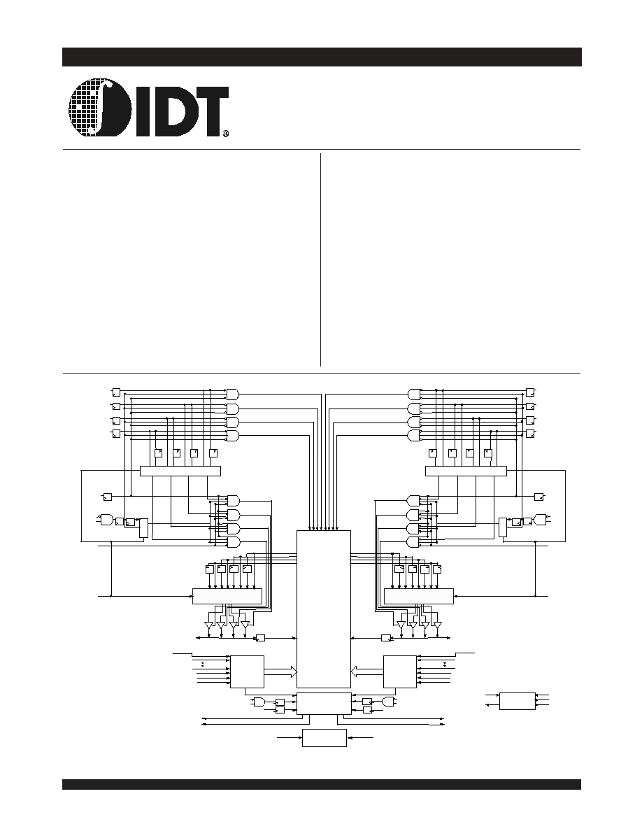
Functional Block Diagram
≠ Data input, address, byte enable and control registers
≠ Self-timed write allows fast cycle time
Separate byte controls for multiplexed bus and bus
matching compatibility
Dual Cycle Deselect (DCD) for Pipelined Output Mode
2.5V (±100mV) power supply for core
LVTTL compatible, selectable 3.3V (±150mV) or 2.5V
(±100mV) power supply for I/Os and control signals on
each port
Industrial temperature range (-40∞C to +85∞C) is
available at 166MHz and 133MHz
Available in a 256-pin Ball Grid Array (BGA), a 208-pin
Plastic Quad Flatpack (PQFP) and 208-pin fine pitch Ball
Grid Array (fpBGA)
Supports JTAG features compliant with IEEE 1149.1
Due to limited pin count JTAG is not supported on the 208-
pin PQFP package
HIGH-SPEED 2.5V
256/128/64K x 36
SYNCHRONOUS
DUAL-PORT STATIC RAM
WITH 3.3V OR 2.5V INTERFACE
IDT70T3519/99/89S
REPEAT
R
A
0R
CNTEN
R
ADS
R
Dout0-8_R
Dout9-17_R
I/O
0R
- I/O
35R
Din_R
ADDR_R
OE
R
BE
3R
BE
2R
BE
1R
BE
0R
R/
W
R
CE
0R
CE
1R
1
0
1/0
FT
/PIPE
R
1a 0a
1b 0b
1c 0c
1d 0d
d
c
b
a
CLK
R
,
Counter/
Address
Reg.
d c b a
0/1
0d 1d
0c 1c
0b 1b
0a 1a
B
W
2
R
B
W
1
R
B
W
0
R
FT
/PIPE
R
Counter/
Address
Reg.
CNTEN
L
ADS
L
REPEAT
L
Dout0-8_L
Dout9-17_L
Dout18-26_L
Dout27-35_L
D out18-26_R
D out27-35_R
B
W
0
L
B
W
1
L
B
W
2
L
B
W
3
L
I/O
0L
- I/O
35L
A
17L(1)
A
0L
Din_L
ADDR_L
OE
L
5666 drw 01
BE
3L
BE
2L
BE
1L
BE
0L
R/
W
L
CE
0L
CE
1L
256/128/64K x 36
MEMORY
ARRAY
CLK
L
a bc d
FT
/PIPE
L
0/1
1d 0d
1c 0c 1b 0b 1a 0a
B
W
3
R
,
JTAG
TCK
TRST
TMS
TDO
TDI
1
0
1/0
0d 1d
0c 1c
0b 1b
0a 1a
a
b
c
d
FT
/PIPE
L
1/0
1/0
INTERRUPT
COLLISION
DETECTION
LOGIC
R /
W
L
CE
0 L
CE1L
R/
W
R
CE
0 R
CE1R
INT
L
COL
L
INT
R
COL
R
ZZ
CONTROL
LOGIC
ZZ
L
(2)
ZZ
R
(2)
A
17R(1)
Features:
True Dual-Port memory cells which allow simultaneous
access of the same memory location
High-speed data access
≠ Commercial: 3.4 (200MHz)/3.6ns (166MHz)/
4.2ns (133MHz)(max.)
≠ Industrial: 3.6ns (166MHz)/4.2ns (133MHz) (max.)
Selectable Pipelined or Flow-Through output mode
Counter enable and repeat features
Dual chip enables allow for depth expansion without
additional logic
Interrupt and Collision Detection Flags
Full synchronous operation on both ports
≠ 5ns cycle time, 200MHz operation (14Gbps bandwidth)
≠ Fast 3.4ns clock to data out
≠ 1.5ns setup to clock and 0.5ns hold on all control, data, and
address inputs @ 200MHz
1. Address A
17
is a NC for the IDT70T3599. Also, Addresses A
17
and A
16
are NC's for the IDT70T3589.
2. The sleep mode pin shuts off all dynamic inputs, except JTAG inputs, when asserted. All static inputs, i.e., PL/FTx and OPTx
and the sleep mode pins themselves (ZZx) are not affected during sleep mode.
NOTES:

6.42
IDT70T3519/99/89S
High-Speed 2.5V 256/128/64K x 36 Dual-Port Synchronous Static RAM Industrial and Commercial Temperature Ranges
2
Description:
The IDT70T3519/99/89 is a high-speed 256/128/64K x 36 bit
synchronous Dual-Port RAM. The memory array utilizes Dual-Port
memory cells to allow simultaneous access of any address from both ports.
Registers on control, data, and address inputs provide minimal setup and
hold times. The timing latitude provided by this approach allows systems
to be designed with very short cycle times. With an input data register, the
IDT70T3519/99/89 has been optimized for applications having unidirec-
tional or bidirectional data flow in bursts. An automatic power down feature,
controlled by CE
0
and CE
1,
permits the on-chip circuitry of each port to
enter a very low standby power mode.
The 70T3519/99/89 can support an operating voltage of either 3.3V
or 2.5V on one or both ports, controllable by the OPT pins. The power
supply for the core of the device (V
DD
) is at 2.5V.

6.42
IDT70T3519/99/89S
High-Speed 2.5V 256/128/64K x 36 Dual-Port Synchronous Static RAM Industrial and Commercial Temperature Ranges
3
Pin Configuration
(3,4,5,6,9)
NOTES:
1. Pin is a NC for IDT70T3599 and IDT70T3589.
2. Pin is a NC for IDT70T3589.
3. All V
DD
pins must be connected to 2.5V power supply.
4. All V
DDQ
pins must be connected to appropriate power supply: 3.3V if OPT pin for that port is set to V
DD
(2.5V), and 2.5V if OPT pin for that port is
set to V
SS
(0V).
5. All V
SS
pins must be connected to ground supply.
6. Package body is approximately 17mm x 17mm x 1.4mm, with 1.0mm ball-pitch.
7. This package code is used to reference the package diagram.
8. This text does not indicate orientation of the actual part-marking.
9. Pins A15 and T15 will be V
REFL
and V
REFR
respectively for future HSTL device.
70T3519/99/89BC
BC-256
(7)
256-Pin BGA
Top View
(8)
E16
I/O
14R
D16
I/O
16R
C16
I/O
16L
B16
NC
A16
NC
A15
NC
B15
I/O
17L
C15
I/O
17R
D15
I/O
15L
E15
I/O
14L
E14
I/O
13L
D14
I/O
15R
D13
V
DD
C12
A
6L
C14
OPT
L
B14
V
DD
A14
A
0L
A12
A
5L
B12
A
4L
C11
ADS
L
D12
V
DDQR
D11
V
DDQR
C10
CLK
L
B11
REPEAT
L
A11
CNTEN
L
D8
V
DDQR
C8
BE
1L
A9
CE
1L
D9
V
DDQL
C9
BE
0L
B9
CE
0L
D10
V
DDQL
C7
A
7L
B8
BE
3L
A8
BE
2L
B13
A
1L
A13
A
2L
A10
OE
L
D7
V
DDQR
B7
A
9L
A7
A
8L
B6
A
12L
C6
A
10L
D6
V
DDQL
A5
A
14L
B5
A
15L
C5
A
13L
D5
V
DDQL
A4
B4
NC
C4
D4
PIPE/
FT
L
A3
NC
B3
TDO
C3
V
SS
D3
I/O
20L
D2
I/O
19R
C2
I/O
19L
B2
NC
A2
TDI
A1
NC
B1
I/O
18L
C1
I/O
18R
D1
I/O
20R
E1
I/O
21R
E2
I/O
21L
E3
I/O
22L
E4
V
DDQL
F1
I/O
23L
F2
I/O
22R
F3
I/O
23R
F4
V
DDQL
G1
I/O
24R
G2
I/O
24L
G3
I/O
25L
G4
V
DDQR
H1
I/O
26L
H2
I/O
25R
H3
I/O
26R
H4
V
DDQR
J1
I/O
27L
J2
I/O
28R
J3
I/O
27R
J4
V
DDQL
K1
I/O
29R
K2
I/O
29L
K3
I/O
28L
K4
V
DDQL
L1
I/O
30L
L2
I/O
31R
L3
I/O
30R
L4
V
DDQR
M1
I/O
32R
M2
I/O
32L
M3
I/O
31L
M4
V
DDQR
N1
I/O
33L
N2
I/O
34R
N3
I/O
33R
N4
PIPE/
FT
R
P1
I/O
35R
P2
I/O
34L
P3
TMS
P4
R1
I/O
35L
R2
NC
R3
TRST
R4
NC
T1
NC
T2
TCK
T3
NC
T4
P5
A
13R
R5
A
15R
P12
A
6R
P8
BE
1R
P9
BE
0R
R8
BE
3R
T8
BE
2R
P10
CLK
R
T11
CNTEN
R
P11
ADS
R
R12
A
4R
T12
A
5R
P13
A
3R
P7
A
7R
R13
A
1R
T13
A
2R
R6
A
12R
T5
A
14R
T14
A
0R
R14
OPT
R
P14
I/O
0L
P15
I/O
0R
R15
NC
T15
NC
T16
NC
R16
NC
P16
I/O
1L
N16
I/O
2R
N15
I/O
1R
N14
I/O
2L
M16
I/O
4L
M15
I/O
3L
M14
I/O
3R
L16
I/O
5R
L15
I/O
4R
L14
I/O
5L
K16
I/O
7L
K15
I/O
6L
K14
I/O
6R
J16
I/O
8L
J15
I/O
7R
J14
I/O
8R
H16
I/O
10R
H15
IO
9L
H14
I/O
9R
G16
I/O
11R
G15
I/O
11L
G14
I/O
10L
F16
I/O
12L
F14
I/O
12R
F15
I/O
13R
R9
CE
0R
R11
REPEAT
R
T6
A
11R
T9
CE
1R
A6
A
11L
B10
R/
W
L
C13
A
3L
P6
A
10R
R10
R/
W
R
R7
A
9R
T10
OE
R
T7
A
8R
,
E5
V
DD
E6
V
DD
E7
INT
L
E8
V
SS
E9
V
SS
E10
V
SS
E11
V
DD
E12
V
DD
E13
V
DDQR
F5
V
DD
F6
NC
F8
V
SS
F9
V
SS
F10
V
SS
F12
V
DD
F13
V
DDQR
G5
V
SS
G6
V
SS
G7
V
SS
G8
V
SS
G9
V
SS
G10
V
SS
G11
V
SS
G12
V
SS
G13
V
DDQL
H5
V
SS
H6
V
SS
H7
V
SS
H8
V
SS
H9
V
SS
H10
V
SS
H11
V
SS
H12
V
SS
H13
V
DDQL
J5
ZZ
R
J6
V
SS
J7
V
SS
J8
V
SS
J9
V
SS
J10
V
SS
J11
V
SS
J12
ZZ
L
J13
V
DDQR
K5
V
SS
K6
V
SS
K7
V
SS
K8
V
SS
L5
V
DD
L6
NC
L7
COL
R
L8
V
SS
M5
V
DD
M6
V
DD
M7
INT
R
M8
V
SS
N5
V
DDQR
N6
V
DDQR
N7
V
DDQL
N8
V
DDQL
K9
V
SS
K10
V
SS
K11
V
SS
K12
V
SS
L9
V
SS
L10
V
SS
L11
V
SS
L12
V
DD
M9
V
SS
M10
V
SS
M11
V
DD
M12
V
DD
N9
V
DDQR
N10
V
DDQR
N11
V
DDQL
N12
V
DDQL
K13
V
DDQR
L13
V
DDQL
M13
V
DDQL
N13
V
DD
F7
COL
L
F11
V
SS
5666 drw 02d
,
06/19/02
A
17R
(1)
A
17L
(1)
A
16L
(2)
A
16R
(2)

6.42
IDT70T3519/99/89S
High-Speed 2.5V 256/128/64K x 36 Dual-Port Synchronous Static RAM Industrial and Commercial Temperature Ranges
4
1
2
3
4
5
6
7
8
9
10
11
12
13
14
15
16
17
18
19
20
21
22
23
24
25
26
27
28
29
30
31
32
33
34
35
36
37
38
39
40
41
42
43
44
45
46
47
48
49
50
51
52
5
3
5
4
5
5
5
6
5
7
5
8
5
9
6
0
6
1
6
2
6
3
6
4
6
5
6
6
6
7
6
8
6
9
7
0
7
1
7
2
7
3
7
4
7
5
7
6
7
7
7
8
7
9
8
0
8
1
8
2
8
3
8
4
8
5
8
6
8
7
8
8
8
9
9
0
9
1
9
2
9
3
9
4
9
5
9
6
9
7
9
8
9
9
1
0
0
1
0
1
1
0
2
1
0
3
1
0
4
156
155
154
153
152
151
150
149
148
147
146
145
144
143
142
141
140
139
138
137
136
135
134
133
132
131
130
129
128
127
126
125
124
123
122
121
120
119
118
117
116
115
114
113
112
111
110
109
108
107
106
105
2
0
8
2
0
7
2
0
6
2
0
5
2
0
4
2
0
3
2
0
2
2
0
1
2
0
0
1
9
9
1
9
8
1
9
7
1
9
6
1
9
5
1
9
4
1
9
3
1
9
2
1
9
1
1
9
0
1
8
9
1
8
8
1
8
7
1
8
6
1
8
5
1
8
4
1
8
3
1
8
2
1
8
1
1
8
0
1
7
9
1
7
8
1
7
7
1
7
6
1
7
5
1
7
4
1
7
3
1
7
2
1
7
1
1
7
0
1
6
9
1
6
8
1
6
7
1
6
6
1
6
5
1
6
4
1
6
3
1
6
2
1
6
1
1
6
0
1
5
9
1
5
8
1
5
7
70T3519/99/89DR
DR-208
(7)
208-Pin PQFP
Top View
(8)
I/O
19L
I/O
19R
I/O
20L
I/O
20R
V
DDQL
V
SS
I/O
21L
I/O
21R
I/O
22L
I/O
22R
V
DDQR
V
SS
I/O
23L
I/O
23R
I/O
24L
I/O
24R
V
DDQL
V
SS
I/O
25L
I/O
25R
I/O
26L
I/O
26R
V
DDQR
ZZ
R
V
DD
V
DD
V
SS
V
SS
V
DDQL
V
SS
I/O
27R
I/O
27L
I/O
28R
I/O
28L
V
DDQR
V
SS
I/O
29R
I/O
29L
I/O
30R
I/O
30L
V
DDQL
V
SS
I/O
31R
I/O
31L
I/O
32R
I/O
32L
V
DDQR
V
SS
I/O
33R
I/O
33L
I/O
34R
I/O
34L
V
S
S
V
D
D
Q
L
I
/
O
3
5
R
I
/
O
3
5
L
P
L
/
F
T
R
N
C
C
O
L
R
I
N
T
R
N
C
N
C
A
1
7
R
(
1
)
A
1
6
R
(
2
)
A
1
5
R
A
1
4
R
A
1
3
R
A
1
2
R
A
1
1
R
A
1
0
R
A
9
R
A
8
R
A
7
R
B
E
3
R
B
E
2
R
B
E
1
R
B
E
0
R
C
E
1
R
C
E
0
R
V
D
D
V
D
D
V
S
S
V
S
S
C
L
K
R
O
E
R
R
/
W
R
A
D
S
R
C
N
T
E
N
R
R
E
P
E
A
T
R
A
6
R
A
5
R
A
4
R
A
3
R
A
2
R
A
1
R
A
0
R
V
D
D
V
S
S
N
C
O
P
T
R
I
/
O
0
L
I
/
O
0
R
V
D
D
Q
L
V
S
S
I/O
16L
I/O
16R
I/O
15L
I/O
15R
V
SS
V
DDQL
I/O
14L
I/O
14R
I/O
13L
I/O
13R
V
SS
V
DDQR
I/O
12L
I/O
12R
I/O
11L
I/O
11R
V
SS
V
DDQL
I/O
10L
I/O
10R
I/O
9L
I/O
9R
V
SS
V
DDQR
V
DD
V
DD
V
SS
V
SS
ZZ
L
V
DDQL
I/O
8R
I/O
8L
I/O
7R
I/O
7L
V
SS
V
DDQR
I/O
6R
I/O
6L
I/O
5R
I/O
5L
V
SS
V
DDQL
I/O
4R
I/O
4L
I/O
3R
I/O
3L
V
SS
V
DDQR
I/O
2R
I/O
2L
I/O
1R
I/O
1L
V
S
S
V
D
D
Q
R
I
/
O
1
8
R
I
/
O
1
8
L
V
S
S
P
L
/
F
T
L
C
O
L
L
I
N
T
L
N
C
N
C
A
1
7
L
(
1
)
A
1
6
L
(
2
)
A
1
5
L
A
1
4
L
A
1
3
L
A
1
2
L
A
1
1
L
A
1
0
L
A
9
L
A
8
L
A
7
L
B
E
3
L
B
E
2
L
B
E
1
L
B
E
0
L
C
E
1
L
C
E
0
L
V
D
D
V
D
D
V
S
S
V
S
S
C
L
K
L
O
E
L
R
/
W
L
A
D
S
L
C
N
T
E
N
L
R
E
P
E
A
T
L
A
6
L
A
5
L
A
4
L
A
3
L
A
2
L
A
1
L
A
0
L
V
D
D
V
D
D
N
C
O
P
T
L
I
/
O
1
7
L
I
/
O
1
7
R
V
D
D
Q
R
V
S
S
5666 drw 02a
,
06/19/02
Pin Configuration
(3,4,5,6,9,10)
(con't.)
NOTES:
3. All V
DD
pins must be connected to 2.5V power supply.
4. All V
DDQ
pins must be connected to appropriate power supply: 3.3V if OPT pin for that port is set to V
DD
(2.5V), and 2.5V if OPT pin for that port is set to V
ss
(0V).
5. All V
SS
pins must be connected to ground supply.
6. Package body is approximately 28mm x 28mm x 3.5mm.
7. This package code is used to reference the package diagram.
8. This text does not indicate orientation of the actual part-marking.
9. Due to limited pin count, JTAG is not supported in the DR-208 package.
10. Pins 162 and 99 will be V
REFL
and V
REFR
respectively for future HSTL device.
1. Pin is a NC for IDT70T3599 and IDT70T3589.
2. Pin is a NC for IDT70T3589.
6.42
IDT70T3519/99/89S
High-Speed 2.5V 256/128/64K x 36 Dual-Port Synchronous Static RAM Industrial and Commercial Temperature Ranges
5
NOTES:
3. All V
DD
pins must be connected to 2.5V power supply.
4. All V
DDQ
pins must be connected to appropriate power supply: 3.3V if OPT pin for that port is set to V
DD
(2.5V), and 2.5V if OPT pin for that port is
set to V
SS
(0V).
5. All V
SS
pins must be connected to ground supply.
6. Package body is approximately 15mm x 15mm x 1.4mm with 0.8mm ball pitch.
7. This package code is used to reference the package diagram.
8. This text does not indicate orientation of the actual part-marking.
9. Pins B14 and R14 will be V
REFL
and V
REFR
respectively for future HSTL device.
Pin Configuration
(3,4,5,6,9)
(con't.)
1. Pin is a NC for IDT70T3599 and IDT70T3589.
2. Pin is a NC for IDT70T3589.
A17
V
SS
B17
I/O
15R
C17
V
SS
D17
I/O
14R
E16
V
SS
E17
I/O
13L
D16
I/O
14L
C16
I/O
15L
B16
I/O
16L
A16
I/O
17L
A15
OPT
L
B15
V
DDQR
C15
I/O
16R
D15
V
DDQL
E15
I/O
13R
E14
I/O
12L
D14
I/O
17R
D13
V
DD
C12
A
6L
C14
V
DD
B14
NC
A14
A
0L
A12
CNTEN
L
B12
A
5L
C11
R/
W
L
D12
A
3L
D11
REPEAT
L
C10
V
SS
B11
ADS
L
A11
CLK
L
D8
BE
0L
C8
BE
3L
A9
BE
1L
D9
V
DD
C9
CE
1L
B9
CE
0L
D10
OE
L
C7
A
10L
B8
BE
2L
A8
A
8L
B13
A
1L
A13
A
4L
A10
V
DD
D7
A
7L
B7
A
9L
A7
A
12L
B6
A
13L
C6
A
14L
D6
A
11L
A5
COL
L
B5
C5
INT
L
D5
A
15L
A4
TDO
B4
TDI
C4
PL/
FT
L
D4
I/O
20L
A3
V
SS
B3
I/O
18R
C3
V
DDQR
D3
I/O
21L
D2
V
SS
C2
I/O
19R
B2
V
SS
A2
I/O
18L
A1
I/O
19L
B1
I/O
20R
C1
V
DDQL
D1
I/O
22L
E1
I/O
23L
E2
I/O
22R
E3
V
DDQR
E4
I/O
21R
F1
V
DDQL
F2
I/O
23R
F3
I/O
24L
F4
V
SS
G1
I/O
26L
G2
V
SS
G3
I/O
25L
G4
I/O
24R
H1
V
DD
H2
I/O
26R
H3
V
DDQR
H4
I/O
25R
J1
V
DDQL
J2
V
DD
J3
V
SS
J4
ZZ
R
K1
I/O
28R
K2
V
SS
K3
I/O
27R
K4
V
SS
L1
I/O
29R
L2
I/O
28L
L3
V
DDQR
L4
I/O
27L
M1
V
DDQL
M2
I/O
29L
M3
I/O
30R
M4
V
SS
N1
I/O
31L
N2
V
SS
N3
I/O
31R
N4
I/O
30L
P1
I/O
32R
P2
I/O
32L
P3
V
DDQR
P4
I/O
35R
R1
V
SS
R2
I/O
33L
R3
I/O
34R
R4
TCK
T1
I/O
33R
T2
I/O
34L
T3
V
DDQL
T4
TMS
U1
V
SS
U2
I/O
35L
U3
PL/
FT
R
U4
COL
R
P5
TRST
R5
U6
A
11R
P12
P8
A
8R
U10
OE
R
P9
BE
1R
R8
BE
2R
T8
BE
3R
U9
V
DD
P10
V
DD
T11
R/
W
R
U8
BE
0R
P11
CLK
R
R12
A
5R
T12
A
6R
U12
A
3R
P13
A
4R
P7
A
12R
R13
A
1R
T13
A
2R
U13
A
0R
R6
A
13R
T5
INT
R
U7
A
7R
U14
V
DD
T14
V
SS
R14
NC
P14
I/O
2L
P15
I/O
3L
R15
V
DDQL
T15
I/O
0R
U15
OPT
R
U16
I/O
0L
U17
I/O
1L
T16
V
SS
T17
I/O
2R
R17
V
DDQR
R16
I/O
1R
P17
I/O
4L
P16
V
SS
N17
I/O
5L
N16
I/O
4R
N15
V
DDQL
N14
I/O
3R
M17
V
DDQR
M16
I/O
5R
M15
I/O
6L
M14
V
SS
L17
I/O
8L
L16
V
SS
L15
I/O
7L
L14
I/O
6R
K17
V
SS
K16
I/O
8R
K15
V
DDQL
K14
I/O
7R
J17
V
DDQR
J16
V
SS
J15
V
DD
J14
ZZ
L
H17
I/O
10R
H16
V
SS
H15
I/O
9R
H14
V
DD
G17
I/O
11R
G16
I/O
10L
G15
V
DDQL
G14
I/O
9L
F17
V
DDQR
F16
I/O
11L
F14
V
SS
70T3519/99/89BF
BF-208
(7)
208-Pin fpBGA
Top View
(8)
F15
I/O
12R
R9
CE
0R
R11
ADS
R
T6
A
14R
T9
CE
1R
A6
B10
V
SS
C13
A
2L
P6
R10
V
SS
R7
A
9R
T10
V
SS
T7
A
10R
U5
A
15R
5666 drw 02c
A
17R
(1)
A
17L
(1)
A
16L
(2)
A
16R
(2)
01/23/03
CNTEN
R

6.42
IDT70T3519/99/89S
High-Speed 2.5V 256/128/64K x 36 Dual-Port Synchronous Static RAM Industrial and Commercial Temperature Ranges
6
Pin Names
Left Port
Right Port
Names
CE
0L
,
CE
1L
CE
0R
,
CE
1R
Chip Enables (Input)
(7)
R/W
L
R/W
R
Read/Write Enable (Input)
OE
L
OE
R
Output Enable (Input)
A
0L
- A
17L
(6)
A
0R
- A
17R
(6)
Address (Input)
I/O
0L
- I/O
35L
I/O
0R
- I/O
35R
Data Input/Output
CLK
L
CLK
R
Clock (Input)
PL/FT
L
PL/FT
R
Pipeline/Flow-Through (Input)
ADS
L
ADS
R
Address Strobe Enable (Input)
CNTEN
L
CNTEN
R
Counter Enable (Input)
REPEAT
L
REPEAT
R
Counter Repeat
(3)
BE
0L
- BE
3L
BE
0R
- BE
3R
Byte Enables (9-bit bytes) (Input)
(7)
V
DDQL
V
DDQR
Power (I/O Bus) (3.3V or 2.5V)
(1)
(Input)
OPT
L
OPT
R
Option for selecting V
DDQX
(1,2)
(Input)
ZZ
L
ZZ
R
Sleep Mode pin
(4)
(Input)
V
DD
Power (2.5V)
(1)
(Input)
V
SS
Ground (0V) (Input)
TDI
(5)
Test Data Input
TDO
(5)
Test Data Output
TCK
(5)
Test Logic Clock (10MHz) (Input)
TMS
(5)
Test Mode Select (Input)
TRST
(5)
Reset (Initialize TAP Controller) (Input)
INT
L
INT
R
Interrupt Flag (Output)
COL
L
COL
R
Collision Alert (Output)
5666 tbl 01
NOTES:
1. V
DD
, OPT
X
, and V
DDQX
must be set to appropriate operating levels prior to
applying inputs on the I/Os and controls for that port.
2. OPT
X
selects the operating voltage levels for the I/Os and controls on that port.
If OPT
X
is set to V
DD
(2.5V), then that port's I/Os and controls will operate at 3.3V
levels and V
DDQX
must be supplied at 3.3V. If OPT
X
is set to V
SS
(0V), then that
port's I/Os and address controls will operate at 2.5V levels and V
DDQX
must be
supplied at 2.5V. The OPT pins are independent of one another--both ports can
operate at 3.3V levels, both can operate at 2.5V levels, or either can operate
at 3.3V with the other at 2.5V.
3. When REPEAT
X
is asserted, the counter will reset to the last valid address loaded
via ADS
X
.
4. The sleep mode pin shuts off all dynamic inputs, except JTAG inputs, when
asserted. All static inputs, i.e., PL/FTx and OPTx and the sleep mode pins
themselves (ZZx) are not affected during sleep mode. It is recommended that
boundry scan not be operated during sleep mode.
5. Due to limited pin count, JTAG is not supported in the DR-208 package.
6. Address A
17x
is a NC for the IDT70T3599. Also, Addresses A
17x
and A
16x
are
NC's for the IDT 70T3589.
7. Chip Enables and Byte Enables are double buffered when PL/FT = V
IH
, i.e., the
signals take two cycles to deselect.

6.42
IDT70T3519/99/89S
High-Speed 2.5V 256/128/64K x 36 Dual-Port Synchronous Static RAM Industrial and Commercial Temperature Ranges
7
NOTES:
1. "H" = V
IH,
"L" = V
IL,
"X" = Don't Care.
2. ADS, CNTEN, REPEAT = V
IH
.
3. OE and ZZ are asynchronous input signals.
4. It is possible to read or write any combination of bytes during a given access. A few representative samples have been illustrated here.
Truth Table I--Read/Write and Enable Control
(1,2,3,4)
OE
CLK
CE
0
CE
1
BE
3
BE
2
BE
1
BE
0
R/W
ZZ
Byte 3
I/O
27-35
Byte 2
I/O
18-26
Byte 1
I/O
9-17
Byte 0
I/O
0-8
MODE
X
H
X
X
X
X
X
X
L
High-Z
High-Z
High-Z
High-Z
Deselected≠Power Down
X
X
L
X
X
X
X
X
L
High-Z
High-Z
High-Z
High-Z
Deselected≠Power Down
X
L
H
H
H
H
H
X
L
High-Z
High-Z
High-Z
High-Z
All Bytes Deselected
X
L
H
H
H
H
L
L
L
High-Z
High-Z
High-Z
D
IN
Write to Byte 0 Only
X
L
H
H
H
L
H
L
L
High-Z
High-Z
D
IN
High-Z
Write to Byte 1 Only
X
L
H
H
L
H
H
L
L
High-Z
D
IN
High-Z
High-Z
Write to Byte 2 Only
X
L
H
L
H
H
H
L
L
D
IN
High-Z
High-Z
High-Z
Write to Byte 3 Only
X
L
H
H
H
L
L
L
L
High-Z
High-Z
D
IN
D
IN
Write to Lower 2 Bytes Only
X
L
H
L
L
H
H
L
L
D
IN
D
IN
High-Z
High-Z
Write to Upper 2 bytes Only
X
L
H
L
L
L
L
L
L
D
IN
D
IN
D
IN
D
IN
Write to All Bytes
L
L
H
H
H
H
L
H
L
High-Z
High-Z
High-Z
D
OUT
Read Byte 0 Only
L
L
H
H
H
L
H
H
L
High-Z
High-Z
D
OUT
High-Z
Read Byte 1 Only
L
L
H
H
L
H
H
H
L
High-Z
D
OUT
High-Z
High-Z
Read Byte 2 Only
L
L
H
L
H
H
H
H
L
D
OUT
High-Z
High-Z
High-Z
Read Byte 3 Only
L
L
H
H
H
L
L
H
L
High-Z
High-Z
D
OUT
D
OUT
Read Lower 2 Bytes Only
L
L
H
L
L
H
H
H
L
D
OUT
D
OUT
High-Z
High-Z
Read Upper 2 Bytes Only
L
L
H
L
L
L
L
H
L
D
OUT
D
OUT
D
OUT
D
OUT
Read All Bytes
H
X
X
X
X
X
X
X
L
High-Z
High-Z
High-Z
High-Z
Outputs Disabled
X
X
X
X
X
X
X
X
X
H
High-Z
High-Z
High-Z
High-Z
Sleep Mode
5666 tbl 02
Truth Table II--Address Counter Control
(1,2)
NOTES:
1. "H" = V
IH,
"L" = V
IL,
"X" = Don't Care.
2. Read and write operations are controlled by the appropriate setting of R/W, CE
0
, CE
1
, BEn and OE.
3. Outputs configured in flow-through output mode: if outputs are in pipelined mode the data out will be delayed by one cycle.
4. ADS and REPEAT are independent of all other memory control signals including CE
0
, CE
1
and BEn
5. The address counter advances if CNTEN = V
IL
on the rising edge of CLK, regardless of all other memory control signals including CE
0
, CE
1
, BEn.
6. When REPEAT is asserted, the counter will reset to the last valid address loaded via ADS. This value is not set at power-up: a known location should be loaded
via ADS during initialization if desired. Any subsequent ADS access during operations will update the REPEAT address location.
Address
Previous
Internal
Address
Internal
Address
Used
CLK
ADS
CNTEN
REPEAT
(6)
I/O
(3)
MODE
An
X
An
L
(4)
X
H
D
I/O
(n)
External Address Used
X
An
An + 1
H
L
(5)
H
D
I/O
(n+1)
Counter Enabled--Internal Address generation
X
An + 1
An + 1
H
H
H
D
I/O
(n+1)
External Address Blocked--Counter disab led (An + 1 reused)
X
X
An
X
X
L
(4)
D
I/O
(n)
Counter Set to last valid ADS load
5666 tbl 03
6.42
IDT70T3519/99/89S
High-Speed 2.5V 256/128/64K x 36 Dual-Port Synchronous Static RAM Industrial and Commercial Temperature Ranges
8
Recommended Operating
Temperature and Supply Voltage
(1)
NOTES:
1. This is the parameter TA. This is the "instant on" case temperature.
Grade
Ambient
Temperature
GND
V
DD
Commercial
0
O
C to +70
O
C
0V
2.5V
+
100mV
Industrial
-40
O
C to +85
O
C
0V
2.5V
+
100mV
5666 tbl 04
Recommended DC Operating
Conditions with V
DDQ
at 3.3V
NOTES:
1. V
IL
(min.) = -1.0V for pulse width less than t
CYC
/2, or 5ns, whichever is less.
2. V
IH
(max.) = V
DDQ
+ 1.0V for pulse width less than t
CYC
/2 or 5ns, whichever is less.
3. To select operation at 3.3V levels on the I/Os and controls of a given port, the OPT pin
for that port must be set to V
DD
(2.5V), and V
DDQX
for that port must be supplied as indicated
above.
Symbol
Parameter
Min.
Typ.
Max.
Unit
V
DD
Core Supply Voltage
2.4
2.5
2.6
V
V
DDQ
I/O Supply Voltage
(3)
3.15
3.3
3.45
V
V
SS
Ground
0
0
0
V
V
IH
Input High Voltage
(Address, Control
&Data I/O Inputs)
(3)
2.0
____
V
DDQ
+ 150mV
(2)
V
V
IH
Input High Voltage
_
JTAG
1.7
____
V
DD
+ 100mV
(2)
V
V
IH
Input High Voltage -
ZZ, OPT, PIPE/FT
V
DD
- 0.2V
____
V
DD
+ 100mV
(2)
V
V
IL
Input Low Voltage
-0.3
(1)
____
0.8
V
V
IL
Input Low Voltage -
ZZ, OPT, PIPE/FT
-0.3
(1)
____
0.2
V
5666 tbl 05b
Recommended DC Operating
Conditions with V
DDQ
at 2.5V
NOTES:
1. V
IL
(min.) = -1.0V for pulse width less than t
CYC
/2 or 5ns, whichever is less.
2. V
IH
(max.) = V
DDQ
+ 1.0V for pulse width less than t
CYC
/2 or 5ns, whichever is less.
3. To select operation at 2.5V levels on the I/Os and controls of a given port, the OPT
pin for that port must be set to V
ss
(0V), and V
DDQX
for that port must be supplied as indicated
above.
Symbol
Parameter
Min.
Typ.
Max.
Unit
V
DD
Core Supply Voltage
2.4
2.5
2.6
V
V
DDQ
I/O Supply Voltage
(3)
2.4
2.5
2.6
V
V
SS
Ground
0
0
0
V
V
IH
Input High Volltage
(Address, Control &
Data I/O Inputs)
(3)
1.7
____
V
DDQ
+ 100mV
(2)
V
V
IH
Input High Voltage
_
JTAG
1.7
____
V
DD
+ 100mV
(2)
V
V
IH
Input High Voltage -
ZZ, OPT, PIPE/FT
V
DD
- 0.2V
____
V
DD
+ 100mV
(2)
V
V
IL
Input Low Voltage
-0.3
(1)
____
0.7
V
V
IL
Input Low Voltage -
ZZ, OPT, PIPE/FT
-0.3
(1)
____
0.2
V
5666 tbl 05a

6.42
IDT70T3519/99/89S
High-Speed 2.5V 256/128/64K x 36 Dual-Port Synchronous Static RAM Industrial and Commercial Temperature Ranges
9
Absolute Maximum Ratings
(1)
Symbol
Rating
Commercial
& Industrial
Unit
V
TERM
(V
DD
)
V
DD
Terminal Voltage
with Respect to GND
-0.5 to 3.6
V
V
TERM
(2)
(V
DDQ
)
V
DDQ
Terminal Voltage
with Respect to GND
-0.3 to V
DDQ
+ 0.3
V
V
TERM
(2)
(INPUTS and I/O's)
Input and I/O Terminal
Voltage with Respect to GND
-0.3 to V
DDQ
+ 0.3
V
T
BIAS
(3)
Temperature Under Bias
-55 to +125
o
C
T
STG
Storage Temperature
-65 to +150
o
C
T
JN
Junction Temperature
+150
o
C
I
OUT
(For V
DDQ
=
3.3V) DC Output Current
50
mA
I
OUT
(For V
DDQ
=
2.5V) DC Output Current
40
mA
5666 tbl 06
NOTES:
1. Stresses greater than those listed under ABSOLUTE MAXIMUM RATINGS may cause
permanent damage to the device. This is a stress rating only and functional operation of the
device at these or any other conditions above those indicated in the operational sections
of this specification is not implied. Exposure to absolute maximum rating conditions for
extended periods may affect reliability.
2. This is a steady-state DC parameter that applies after the power supply has reached its
nominal operating value. Power sequencing is not necessary; however, the voltage on
any Input or I/O pin cannot exceed V
DDQ
during power supply ramp up.
3. Ambient Temperature under DC Bias. No AC Conditions. Chip Deselected.
NOTES:
1. These parameters are determined by device characterization, but are not
production tested.
2. 3dV references the interpolated capacitance when the input and output switch
from 0V to 3V or from 3V to 0V.
3. C
OUT
also references C
I/O
.
Capacitance
(1)
(T
A
= +25∞C, F = 1.0MH
Z
) PQFP ONLY
Symbol
Parameter
Conditions
(2)
Max.
Unit
C
IN
Input Capacitance
V
IN
= 3dV
8
pF
C
OUT
(3)
Output Capacitance
V
OUT
= 3dV
10.5
pF
5666 tbl 07
DC Electrical Characteristics Over the Operating
Temperature and Supply Voltage Range
(V
DD
= 2.5V ± 100mV)
Symbol
Parameter
Test Conditions
70T3519/99/89S
Unit
Min.
Max.
|I
LI
|
Input Leakage Current
(1)
V
DDQ
= Max., V
IN
= 0V to V
DDQ
___
10
µA
|I
LI
|
JTAG & ZZ Input Leakage Current
(1,2)
V
DD =
Max.
,
V
IN
= 0V to V
DD
___
±30
µA
|I
LO
|
Output Leakage Current
(1,3)
CE
0
= V
IH
or CE
1
= V
IL
, V
OUT
= 0V to V
DDQ
___
10
µA
V
OL
(3.3V)
Output Low Voltage
(1)
I
OL
= +4mA, V
DDQ
= Min.
___
0.4
V
V
OH
(3.3V)
Output High Voltage
(1)
I
OH
= -4mA, V
DDQ
= Min.
2.4
___
V
V
OL
(2.5V)
Output Low Voltage
(1)
I
OL
= +2mA, V
DDQ
= Min.
___
0.4
V
V
OH
(2.5V)
Output High Voltage
(1)
I
OH
= -2mA, V
DDQ
= Min.
2.0
___
V
5666 tbl 08
NOTES:
1. V
DDQ
is selectable (3.3V/2.5V) via OPT pins. Refer to p.5 for details.
2. Applicable only for TMS, TDI and TRST inputs.
3. Outputs tested in tri-state mode.
6.42
IDT70T3519/99/89S
High-Speed 2.5V 256/128/64K x 36 Dual-Port Synchronous Static RAM Industrial and Commercial Temperature Ranges
10
DC Electrical Characteristics Over the Operating
Temperature and Supply Voltage Range
(3)
(V
DD
= 2.5V ± 100mV)
NOTES:
1. At f = f
MAX
, address and control lines (except Output Enable) are cycling at the maximum frequency clock cycle of 1/t
CYC
, using "AC TEST CONDITIONS".
2. f = 0 means no address, clock, or control lines change. Applies only to input at CMOS level standby.
3. Port "A" may be either left or right port. Port "B" is the opposite from port "A".
4. V
DD
= 2.5V, T
A
= 25∞C for Typ, and are not production tested. I
DD DC
(f=0)
= 15mA (Typ).
5. CE
X
= V
IL
means CE
0X
= V
IL
and CE
1X
= V
IH
CE
X
= V
IH
means CE
0X
= V
IH
or CE
1X
= V
IL
CE
X
< 0.2V means CE
0X
< 0.2V and CE
1X
> V
DD
- 0.2V
CE
X
> V
DD
- 0.2V means CE
0X
> V
DD
- 0.2V or CE
1X
- 0.2V
"X" represents "L" for left port or "R" for right port.
6. I
SB
1
, I
SB
2
and
I
SB
4
will all reach full standby levels
(
I
SB
3)
on the appropriate port(s) if ZZ
L
and/or ZZ
R
= V
IH
.
7. 166MHz I-Temp is not available in the BF-208 package.
8. 200Mhz is not available in the BF-208 and DR-208 packages.
70T3519/99/89
S200
Com'l Only
(8)
70T3519/99/89
S166
Com'l
& Ind
(7)
70T3519/99/89
S133
Com'l
& Ind
Symbol
Parameter
Test Condition
Version
Typ.
(4)
Max.
Typ.
(4)
Max.
Typ.
(4)
Max.
Unit
I
DD
Dynamic Operating
Current (Both
Ports Active)
CE
L
and CE
R
= V
IL
,
Outputs Disabled,
f = f
MAX
(1)
COM'L
S
375
525
320
450
260
370
mA
IND
S
___
___
320
510
260
450
I
SB1
(6)
Standby Current
(Both Ports - TTL
Level Inputs)
CE
L
= CE
R
= V
IH
f = f
MAX
(1)
COM'L
S
205
270
175
230
140
190
mA
IND
S
___
___
175
275
140
235
I
SB2
(6)
Standby Current
(One Port - TTL
Level Inputs)
CE
"A"
= V
IL
and CE
"B"
= V
IH
(5)
Active Port Outputs Disabled,
f=f
MAX
(1)
COM'L
S
300
375
250
325
200
250
mA
IND
S
___
___
250
365
200
310
I
SB3
Full Standby Current
(Both Ports - CMOS
Level Inputs)
Both Ports CE
L
and
CE
R
> V
DDQ
- 0.2V, V
IN
> V
DDQ
- 0.2V
or V
IN
< 0.2V, f = 0
(2)
COM'L
S
5
15
5
15
5
15
mA
IND
S
___
___
5
20
5
20
I
SB4
(6)
Full Standby Current
(One Port - CMOS
Level Inputs)
CE
"A"
< 0.2V and CE
"B"
> V
DDQ
- 0.2V
(5)
V
IN
> V
DDQ
- 0.2V or V
IN
< 0.2V
Active Port, Outputs Disabled, f = f
MAX
(1)
COM'L
S
300
375
250
325
200
250
mA
IND
S
___
___
250
365
200
310
Izz
Sleep Mode Current
(Both Ports - TTL
Level Inputs)
ZZ
L =
ZZ
R =
V
IH
f=f
MAX
(1)
COM'L
S
5
15
5
15
5
15
mA
IND
S
___
___
5
20
5
20
5666 tbl 09

6.42
IDT70T3519/99/89S
High-Speed 2.5V 256/128/64K x 36 Dual-Port Synchronous Static RAM Industrial and Commercial Temperature Ranges
11
AC Test Conditions
(V
DDQ
- 3.3V/2.5V)
Figure 1. AC Output Test load.
Input Pulse Levels (Address & Controls)
Input Pulse Levels (I/Os)
Input Rise/Fall Times
Input Timing Reference Levels
Output Reference Levels
Output Load
GND to 3
.
0V/GND to 2.4V
GND to 3.0V/GND to 2.4V
2ns
1.5V/1.25V
1.5V/1.25V
Figure 1
5666 tbl 10
1.5V/1.25
50
50
5666 drw 03
10pF
(Tester)
DATA
OUT
,
Capacitance (pF) from AC Test Load
5666 drw 04
tCD
(Typical, ns)
6.42
IDT70T3519/99/89S
High-Speed 2.5V 256/128/64K x 36 Dual-Port Synchronous Static RAM Industrial and Commercial Temperature Ranges
12
AC Electrical Characteristics Over the Operating Temperature Range
(Read and Write Cycle Timing)
(2,3)
(V
DD
= 2.5V ± 100mV, T
A
= 0∞C to +70∞C)
NOTES:
1. The Pipelined output parameters (t
CYC2
, t
CD2
) apply to either or both left and right ports when FT/PIPE
X
= V
DD
(2.5V). Flow-through parameters (t
CYC1
, t
CD1
)
apply when FT/PIPE = V
ss
(0V) for that port.
2. All input signals are synchronous with respect to the clock except for the asynchronous Output Enable (OE), FT/PIPE and OPT. FT/PIPE and OPT should be
treated as DC signals, i.e. steady state during operation.
3. These values are valid for either level of V
DDQ
(3.3V/2.5V). See page 6 for details on selecting the desired operating voltage levels for each port.
4. 166MHz I-Temp is not available in the BF-208 package.
5. 200Mhz is not available in the BF-208 and DR-208 packages.
6. Guaranteed by design (not production tested).
70T3519/99/89
S200
Com'l Only
(5)
70T3519/99/89
S166
Com'l
& Ind
(4)
70T3519/99/89
S133
Com'l
& Ind
Symbol
Parameter
Min.
Max.
Min.
Max.
Min.
Max.
Unit
t
CYC1
Clock Cycle Time (Flow-Through)
(1)
15
____
20
____
25
____
ns
t
CYC2
Clock Cycle Time (Pipelined)
(1)
5
____
6
____
7.5
____
ns
t
CH1
Clock High Time (Flow-Through)
(1)
6
____
8
____
10
____
ns
t
CL1
Clock Low Time (Flow-Through)
(1)
6
____
8
____
10
____
ns
t
CH2
Clock High Time (Pipelined)
(2)
2
____
2.4
____
3
____
ns
t
CL2
Clock Low Time (Pipelined)
(1)
2
____
2.4
____
3
____
ns
t
SA
Address Setup Time
1.5
____
1.7
____
1.8
____
ns
t
HA
Address Hold Time
0.5
____
0.5
____
0.5
____
ns
t
SC
Chip Enable Setup Time
1.5
____
1.7
____
1.8
____
ns
t
HC
Chip Enable Hold Time
0.5
____
0.5
____
0.5
____
ns
t
SB
Byte Enable Setup Time
1.5
____
1.7
____
1.8
____
ns
t
HB
Byte Enable Hold Time
0.5
____
0.5
____
0.5
____
ns
t
SW
R/W Setup Time
1.5
____
1.7
____
1.8
____
ns
t
HW
R/W Hold Time
0.5
____
0.5
____
0.5
____
ns
t
SD
Input Data Setup Time
1.5
____
1.7
____
1.8
____
ns
t
HD
Input Data Hold Time
0.5
____
0.5
____
0.5
____
ns
t
SAD
ADS
Setup Time
1.5
____
1.7
____
1.8
____
ns
t
HAD
ADS
Hold Time
0.5
____
0.5
____
0.5
____
ns
t
SCN
CNTEN
Setup Time
1.5
____
1.7
____
1.8
____
ns
t
HCN
CNTEN
Hold Time
0.5
____
0.5
____
0.5
____
ns
t
SRPT
REPEAT
Setup Time
1.5
____
1.7
____
1.8
____
ns
t
HRPT
REPEAT
Hold Time
0.5
____
0.5
____
0.5
____
ns
t
OE
Output Enable to Data Valid
____
4.4
____
4.4
____
4.6
ns
t
OLZ
(6)
Output Enable to Output Low-Z
1
____
1
____
1
____
ns
t
OHZ
(6)
Output Enable to Output High-Z
1
3.4
1
3.6
1
4.2
ns
t
CD1
Clock to Data Valid (Flow-Through)
(1)
____
10
____
12
____
15
ns
t
CD2
Clock to Data Valid (Pipelined)
(1)
____
3.4
____
3.6
____
4.2
ns
t
DC
Data Output Hold After Clock High
1
____
1
____
1
____
ns
t
CKHZ
(6)
Clock High to Output High-Z
1
3.4
1
3.6
1
4.2
ns
t
CKLZ
(6)
Clock High to Output Low-Z
1
____
1
____
1
____
ns
t
INS
Interrupt Flag Set Time
____
7
____
7
____
7
ns
t
INR
Interrupt Flag Reset Time
____
7
____
7
____
7
ns
t
COLS
Collision Flag Set Time
____
3.4
____
3.6
____
4.2
ns
t
COLR
Collision Flag Reset Time
____
3.4
____
3.6
____
4.2
ns
t
ZZSC
Sleep Mode Set Cycles
2
____
2
____
2
____
cycles
t
ZZRC
Sleep Mode Recovery Cycles
3
____
3
____
3
____
cycles
Port-to-Port Delay
t
CO
Clock-to-Clock Offset
4
____
5
____
6
____
ns
t
OFS
Clock-to-Clock Offset for Collision Detection
Please refer to Collision Detection Timing Table on Page 21
5666 tbl 11
6.42
IDT70T3519/99/89S
High-Speed 2.5V 256/128/64K x 36 Dual-Port Synchronous Static RAM Industrial and Commercial Temperature Ranges
13
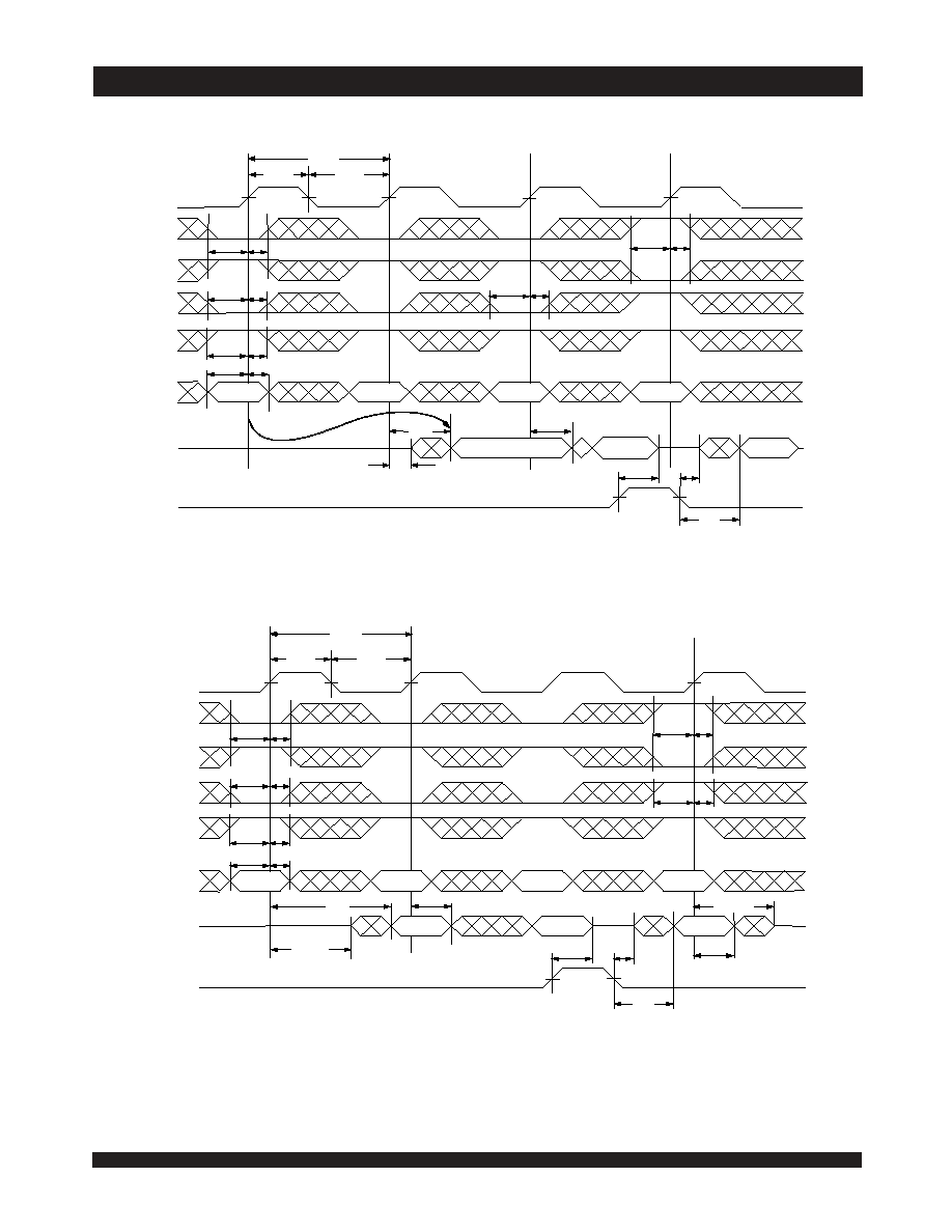
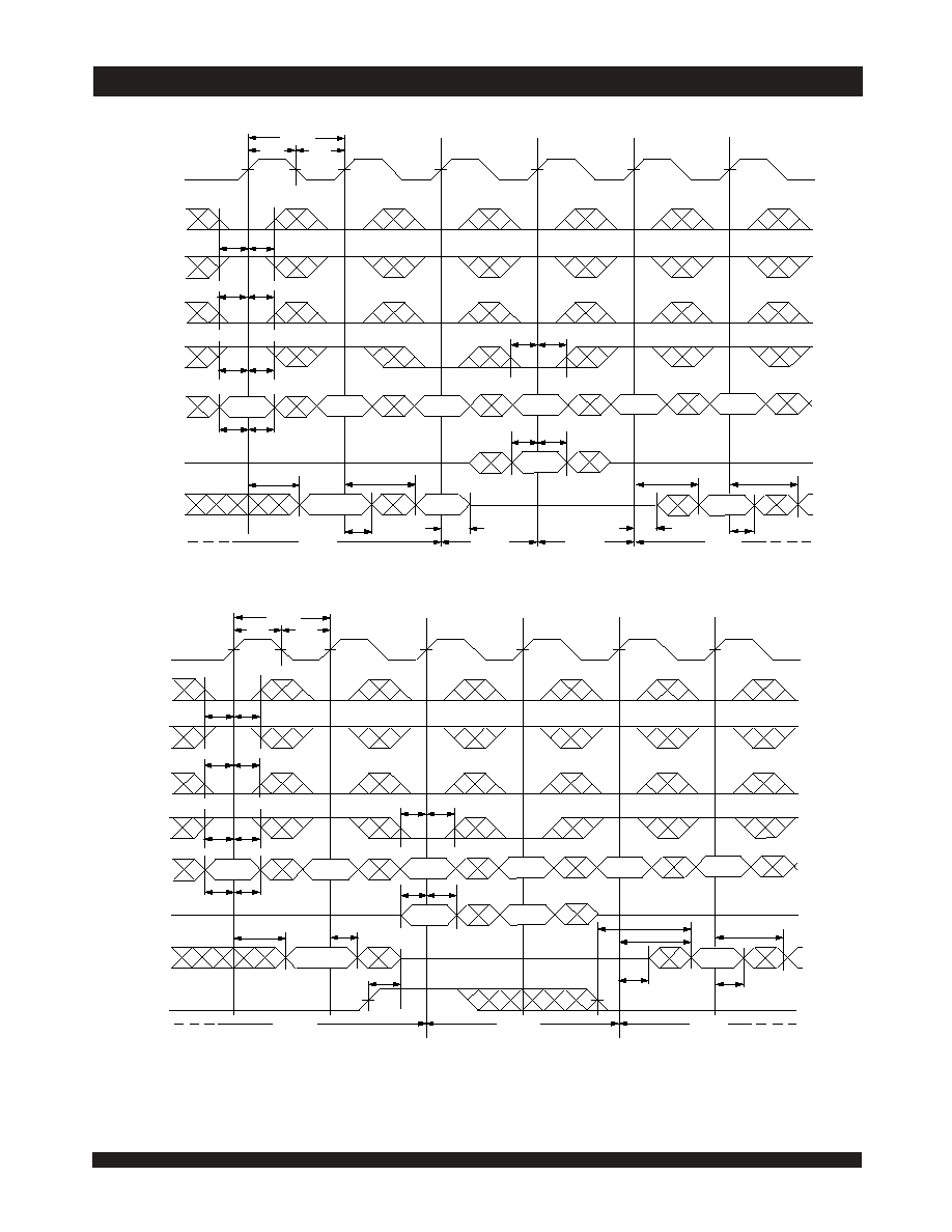
An
An + 1
An + 2
An + 3
t
CYC2
t
CH2
t
CL2
R/
W
ADDRESS
CE
0
CLK
CE
1
BE
n
(3)
DATA
OUT
OE
t
CD2
t
CKLZ
Qn
Qn + 1
Qn + 2
t
OHZ
t
OLZ
t
OE
5666 drw 05
(1)
(1)
t
SC
t
HC
t
SB
t
HB
t
SW
t
HW
t
SA
t
HA
t
DC
t
SC
t
HC
t
SB
t
HB
(4)
(1 Latency)
(5)
(5)
Timing Waveform of Read Cycle for Pipelined Operation
(FT/PIPE
'X'
= V
IH
)
(1,2)
NOTES:
1. OE is asynchronously controlled; all other inputs depicted in the above waveforms are synchronous to the rising clock edge.
2. ADS = V
IL
, CNTEN and REPEAT = V
IH
.
3. The output is disabled (High-Impedance state) by CE
0
= V
IH
, CE
1
= V
IL
, BE
n
= V
IH
following the next rising edge of the clock. Refer to
Truth Table 1.
4. Addresses do not have to be accessed sequentially since ADS = V
IL
constantly loads the address on the rising edge of the CLK; numbers
are for reference use only.
5. If BE
n
was HIGH, then the appropriate Byte of DATA
OUT
for Qn + 2 would be disabled (High-Impedance state).
6. "x" denotes Left or Right port. The diagram is with respect to that port.
Timing Waveform of Read Cycle for Flow-through Output
(FT/PIPE
"X"
= V
IL
)
(1,2,6)
An
An + 1
An + 2
An + 3
t
CYC1
t
CH1
t
CL1
R/
W
ADDRESS
DATA
OUT
CE
0
CLK
OE
t
SC
t
HC
t
CD1
t
CKLZ
Qn
Qn + 1
Qn + 2
t
OHZ
t
OLZ
t
OE
t
CKHZ
5666 drw 06
(5)
(1)
CE
1
BE
n
(3)
t
SB
t
HB
t
SW
t
HW
t
SA
t
HA
t
DC
t
DC
(4)
t
SC
t
HC
t
SB
t
HB

6.42
IDT70T3519/99/89S
High-Speed 2.5V 256/128/64K x 36 Dual-Port Synchronous Static RAM Industrial and Commercial Temperature Ranges
14
t
SC
t
HC
CE
0(B1)
ADDRESS
(B1)
A
0
A
1
A
2
A
3
A
4
A
5
t
SA
t
HA
CLK
Q
0
Q
1
Q
3
DATA
OUT(B1)
t
CH2
t
CL2
t
CYC2
ADDRESS
(B2)
A
0
A
1
A
2
A
3
A
4
A
5
t
SA
t
HA
CE
0(B2)
DATA
OUT(B2)
Q
2
Q
4
t
CD2
t
CD2
t
CKHZ
t
CD2
t
CKLZ
t
DC
t
CKHZ
t
CD2
t
CKLZ
t
SC
t
HC
t
CKHZ
t
CKLZ
t
CD2
A
6
A
6
t
DC
t
SC
t
HC
t
SC
t
HC
5666 drw 07
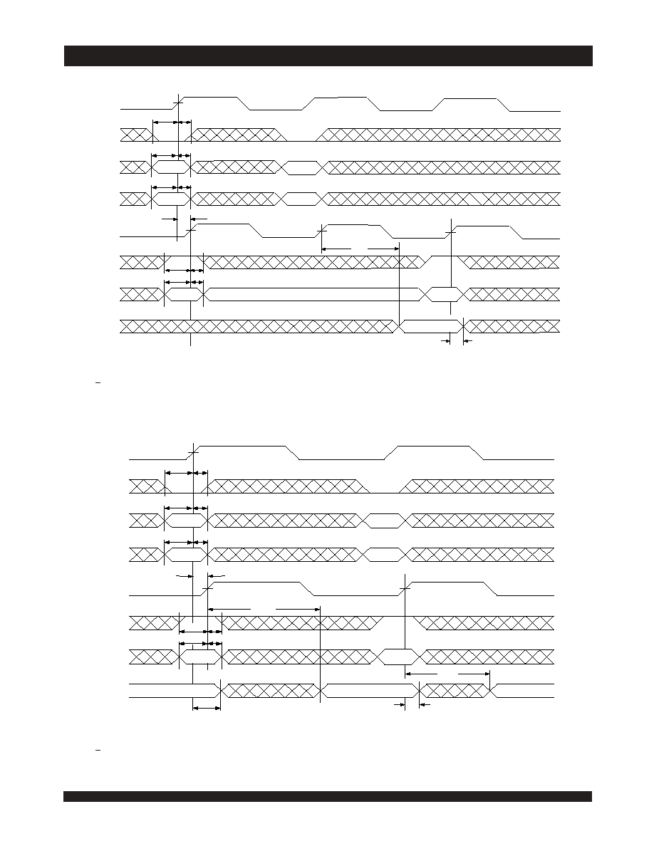
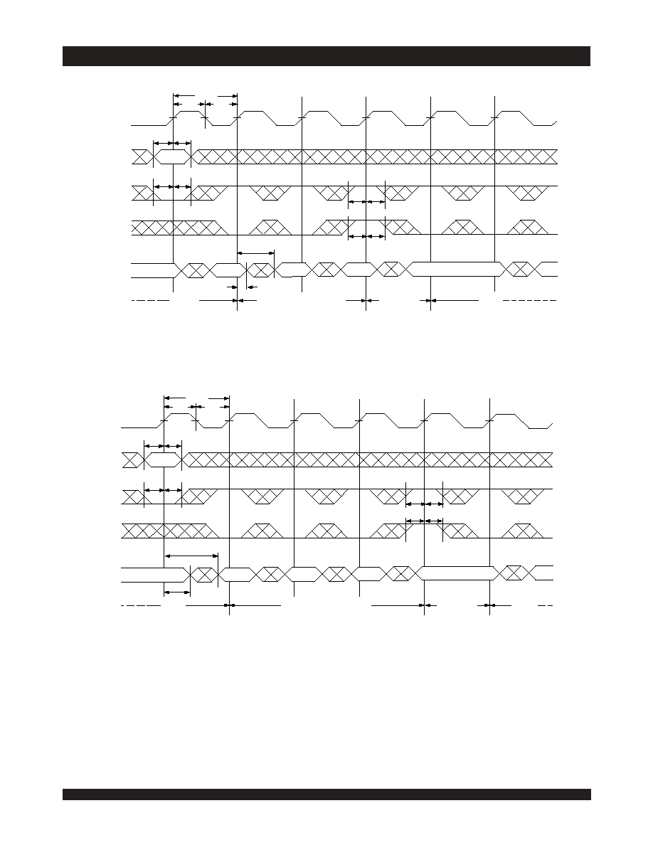
Timing Waveform of a Multi-Device Pipelined Read
(1,2)
NOTES:
1. B1 Represents Device #1; B2 Represents Device #2. Each Device consists of one IDT70T3519/99/89 for this waveform,
and are setup for depth expansion in this example. ADDRESS
(B1)
= ADDRESS
(B2)
in this situation.
2. BE
n
, OE, and ADS = V
IL
; CE
1(B1)
, CE
1(B2)
, R/W, CNTEN, and REPEAT = V
IH
.
Timing Waveform of a Multi-Device Flow-Through Read
(1,2)
t
SC
t
HC
CE
0(B1)
ADDRESS
(B1)
A
0
A
1
A
2
A
3
A
4
A
5
t
SA
t
HA
CLK
5666 drw 08
D
0
D
3
t
CD1
t
CKLZ
t
CKHZ
(1)
(1)
D
1
DATA
OUT(B1)
t
CH1
t
CL1
t
CYC1
(1)
ADDRESS
(B2)
A
0
A
1
A
2
A
3
A
4
A
5
t
SA
t
HA
CE
0(B2)
DATA
OUT(B2)
D
2
D
4
t
CD1
t
CD1
t
CKHZ
t
DC
t
CD1
t
CKLZ
t
SC
t
HC
(1)
t
CKHZ
(1)
t
CKLZ
(1)
t
CD1
A
6
A
6
t
DC
t
SC
t
HC
t
SC
t
HC
D
5
t
CD1
t
CKLZ
(1)
t
CKHZ
(1)
6.42
IDT70T3519/99/89S
High-Speed 2.5V 256/128/64K x 36 Dual-Port Synchronous Static RAM Industrial and Commercial Temperature Ranges
15
CLK
"A"
R/
W
"A"
ADDRESS
"A"
DATA
IN"A"
CLK
"B"
R/
W
"B"
ADDRESS
"B"
DATA
OUT"B"
t
SW
t
HW
t
SA
t
HA
t
SD
t
HD
t
SW
t
HW
t
SA
t
HA
t
CO
(3)
t
CD2
NO
MATCH
VALID
NO
MATCH
MATCH
MATCH
VALID
5666 drw 09
t
DC
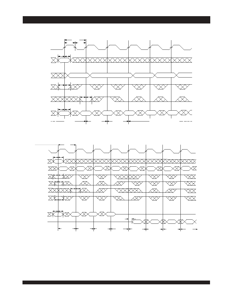
Timing Waveform of Left Port Write to Pipelined Right Port Read
(1,2,4)
NOTES:
1. CE
0
, BE
n
, and ADS = V
IL
; CE
1
, CNTEN, and REPEAT = V
IH
.
2. OE = V
IL
for Port "B", which is being read from. OE = V
IH
for Port "A", which is being written to.
3. If t
CO
< minimum specified, then data from Port "B" read is not valid until following Port "B" clock cycle (ie, time from write to valid read on opposite port will be
t
CO
+ 2 t
CYC2
+ t
CD2
). If t
CO
> minimum, then data from Port "B" read is available on first Port "B" clock cycle (ie, time from write to valid read on opposite port
will be t
CO
+ t
CYC2
+ t
CD2
).
4. All timing is the same for Left and Right ports. Port "A" may be either Left or Right port. Port "B" is the opposite of Port "A"
Timing Waveform with Port-to-Port Flow-Through Read
(1,2,4)
DATA
IN "A"
CLK
"B"
R/
W
"B"
ADDRESS
"A"
R/
W
"A"
CLK
"A"
ADDRESS
"B"
NO
MATCH
MATCH
NO
MATCH
MATCH
VALID
t
CD1
t
DC
DATA
OUT "B"
5666 drw 10
VALID
VALID
t
SW
t
HW
t
SA
t
HA
t
SD
t
HD
t
HW
t
CD1
t
CO
t
DC
t
SA
t
SW
t
HA
(3)
NOTES:
1. CE
0
, BEn, and ADS = V
IL
; CE
1
, CNTEN, and REPEAT = V
IH
.
2. OE = V
IL
for the Right Port, which is being read from. OE = V
IH
for the Left Port, which is being written to.
3. If t
CO
< minimum specified, then data from Port "B" read is not valid until following Port "B" clock cycle (i.e., time from write to valid read on opposite port will be
t
CO
+ t
CYC
+ t
CD1
). If t
CO
> minimum, then data from Port "B" read is available on first Port "B" clock cycle (i.e., time from write to valid read on opposite port will
be t
CO
+ t
CD1
).
4. All timing is the same for both left and right ports. Port "A" may be either left or right port. Port "B" is the opposite of Port "A".
6.42
IDT70T3519/99/89S
High-Speed 2.5V 256/128/64K x 36 Dual-Port Synchronous Static RAM Industrial and Commercial Temperature Ranges
16
R/
W
ADDRESS
An
An +1
An + 2
An + 2
An + 3
An + 4
DATA
IN
Dn + 2
CE
0
CLK
5666 drw 11
Qn
Qn + 3
DATA
OUT
CE
1
BE
n
t
CD2
t
CKHZ
t
CKLZ
t
CD2
t
SC
t
HC
t
SB
t
HB
t
SW
t
HW
t
SA
t
HA
t
CH2
t
CL2
t
CYC2
READ
NOP
READ
t
SD
t
HD
(3)
(1)
t
SW
t
HW
WRITE
(4)
Timing Waveform of Pipelined Read-to-Write-to-Read
(OE = V
IL
)
(2)
NOTES:
1. Output state (High, Low, or High-impedance) is determined by the previous cycle control signals.
2. CE
0
, BE
n
, and ADS = V
IL
; CE
1
, CNTEN, and REPEAT = V
IH
. "NOP" is "No Operation".
3. Addresses do not have to be accessed sequentially since ADS = V
IL
constantly loads the address on the rising edge of the CLK; numbers
are for reference use only.
4. "NOP" is "No Operation." Data in memory at the selected address may be corrupted and should be re-written to guarantee data integrity.
R/
W
ADDRESS
An
An +1
An + 2
An + 3
An + 4
An + 5
DATA
IN
Dn + 3
Dn + 2
CE
0
CLK
5666 drw 12
DATA
OUT
Qn
Qn + 4
CE
1
BE
n
OE
t
CH2
t
CL2
t
CYC2
t
CKLZ
t
CD2
t
OHZ
t
CD2
t
SD
t
HD
READ
WRITE
READ
t
SC
t
HC
t
SB
t
HB
t
SW
t
HW
t
SA
t
HA
(3)
(1)
t
SW
t
HW
(4)
Timing Waveform of Pipelined Read-to-Write-to-Read ( OE Controlled)
(2)
NOTES:
1. Output state (High, Low, or High-impedance) is determined by the previous cycle control signals.
2. CE
0
, BE
n
, and ADS = V
IL
; CE
1
, CNTEN, and REPEAT = V
IH
.
3. Addresses do not have to be accessed sequentially since ADS = V
IL
constantly loads the address on the rising edge of the CLK; numbers are for reference
use only.
4. This timing does not meet requirements for fastest speed grade. This waveform indicates how logically it could be done if timing so allows.
6.42
IDT70T3519/99/89S
High-Speed 2.5V 256/128/64K x 36 Dual-Port Synchronous Static RAM Industrial and Commercial Temperature Ranges
17
Timing Waveform of Flow-Through Read-to-Write-to-Read ( OE = V
IL
)
(2)
Timing Waveform of Flow-Through Read-to-Write-to-Read (OE Controlled)
(2)
NOTES:
1. Output state (High, Low, or High-impedance) is determined by the previous cycle control signals.
2. CE
0
, BEn, and ADS = V
IL
; CE
1
, CNTEN, and REPEAT = V
IH
.
3. Addresses do not have to be accessed sequentially since ADS = V
IL
constantly loads the address on the rising edge of the CLK; numbers are for
reference use only.
4. "NOP" is "No Operation." Data in memory at the selected address may be corrupted and should be re-written to guarantee data integrity.
R/
W
ADDRESS
An
An +1
An + 2
An + 2
An + 3
An + 4
DATA
IN
Dn + 2
CE
0
CLK
5666 drw 13
Qn
DATA
OUT
CE
1
BE
n
t
CD1
Qn + 1
t
CH1
t
CL1
t
CYC1
t
SD
t
HD
t
CD1
t
CD1
t
DC
t
CKHZ
Qn + 3
t
CD1
t
DC
t
SC
t
HC
t
SB
t
HB
t
SW
t
HW
t
SA
t
HA
READ
NOP
READ
t
CKLZ
(3)
(1)
t
SW
t
HW
WRITE
(5)
R/
W
ADDRESS
An
An +1
An + 2
An + 3
An + 4
An + 5
(3)
DATA
IN
Dn + 2
CE
0
CLK
5666 drw 14
Qn
DATA
OUT
CE
1
BE
n
t
CD1
t
CH1
t
CL1
t
CYC1
t
SD
t
HD
t
CD1
t
DC
Qn + 4
t
CD1
t
DC
t
SC
t
HC
t
SB
t
HB
t
SW
t
HW
t
SA
t
HA
READ
WRITE
READ
t
CKLZ
(1)
Dn + 3
t
OHZ
t
SW
t
HW
OE
t
OE
6.42
IDT70T3519/99/89S
High-Speed 2.5V 256/128/64K x 36 Dual-Port Synchronous Static RAM Industrial and Commercial Temperature Ranges
18
ADDRESS
An
CLK
DATA
OUT
Qx - 1
(2)
Qx
Qn
Qn + 2
(2)
Qn + 3
ADS
CNTEN
t
CYC2
t
CH2
t
CL2
5666 drw 15
t
SA
t
HA
t
SAD
t
HAD
t
CD2
t
DC
READ
EXTERNAL
ADDRESS
READ WITH COUNTER
COUNTER
HOLD
t
SAD
t
HAD
t
SCN
t
HCN
READ
WITH
COUNTER
Qn + 1
Timing Waveform of Pipelined Read with Address Counter Advance
(1)
NOTES:
1. CE
0
, OE, BEn = V
IL
; CE
1
, R/W, and REPEAT = V
IH
.
2. If there is no address change via ADS = V
IL
(loading a new address) or CNTEN = V
IL
(advancing the address), i.e. ADS = V
IH
and CNTEN = V
IH
, then
the data output remains constant for subsequent clocks.
Timing Waveform of Flow-Through Read with Address Counter Advance
(1)
ADDRESS
An
CLK
DATA
OUT
Qx
(2)
Qn
Qn + 1
Qn + 2
Qn + 3
(2)
Qn + 4
ADS
CNTEN
t
CYC1
t
CH1
t
CL1
5666 drw 16
t
SA
t
HA
t
SAD
t
HAD
READ
EXTERNAL
ADDRESS
READ WITH COUNTER
COUNTER
HOLD
t
CD1
t
DC
t
SAD
t
HAD
t
SCN
t
HCN
READ
WITH
COUNTER
6.42
IDT70T3519/99/89S
High-Speed 2.5V 256/128/64K x 36 Dual-Port Synchronous Static RAM Industrial and Commercial Temperature Ranges
19
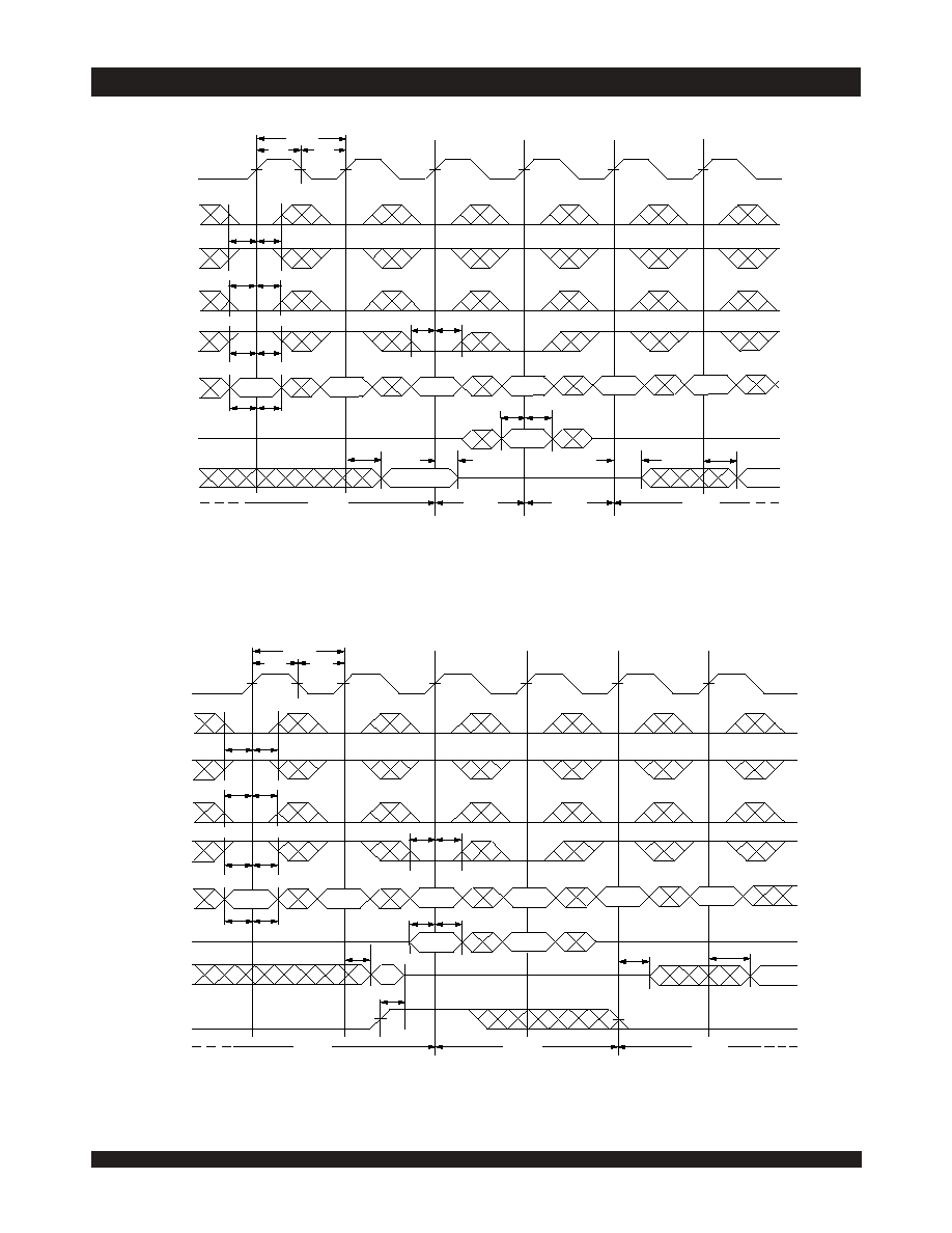
ADDRESS
An
t
CYC2
CLK
DATA
IN
R/
W
REPEAT
5666 drw 18
INTERNAL
(3)
ADDRESS
ADS
CNTEN
WRITE TO
ADS
ADDRESS
An
ADVANCE
COUNTER
WRITE TO
An+1
ADVANCE
COUNTER
WRITE TO
An+2
HOLD
COUNTER
WRITE TO
An+2
REPEAT
READ LAST
ADS
ADDRESS
An
DATA
OUT
t
SA
t
HA
,
An
t
SAD
t
HAD
t
SW
t
HW
t
SCN
t
HCN
t
SRPT
t
HRPT
t
SD
t
HD
t
CD1
An+1
An+2
An+2
An
An+1
An+2
An+2
D
0
D
1
D
2
D
3
An
An+1
An+2
An+2
ADVANCE
COUNTER
READ
An+1
ADVANCE
COUNTER
READ
An+2
HOLD
COUNTER
READ
An+2
(4)
Timing Waveform of Write with Address Counter Advance
(Flow-through or Pipelined Inputs)
(1)
Timing Waveform of Counter Repeat
(2,6)
ADDRESS
An
CLK
DATA
IN
Dn
Dn + 1
Dn + 1
Dn + 2
ADS
CNTEN
t
CH2
t
CL2
t
CYC2
5666 drw 17
INTERNAL
(3)
ADDRESS
An
(7)
An + 1
An + 2
An + 3
An + 4
Dn + 3
Dn + 4
t
SA
t
HA
t
SAD
t
HAD
WRITE
COUNTER HOLD
WRITE WITH COUNTER
WRITE
EXTERNAL
ADDRESS
WRITE
WITH COUNTER
t
SD
t
HD
t
SCN
t
HCN
NOTES:
1. CE
0
, BE
n
, and R/W = V
IL
; CE
1
and REPEAT = V
IH
.
2. CE
0
, BE
n
= V
IL
; CE
1
= V
IH
.
3. The "Internal Address" is equal to the "External Address" when ADS = V
IL
and equals the counter output when ADS = V
IH
.
4. No dead cycle exists during REPEAT operation. A READ or WRITE cycle may be coincidental with the counter REPEAT cycle: Address loaded by last valid
ADS
load will be accessed. For more information on REPEAT function refer to Truth Table II.
5. CNTEN = V
IL
advances Internal Address from `An' to `An +1'. The transition shown indicates the time required for the counter to advance. The `An +1'Address is
written to during this cycle.
6. For Pipelined Mode user should add 1 cycle latency for outputs as per timing waveform of read cycle for pipelined operations.

6.42
IDT70T3519/99/89S
High-Speed 2.5V 256/128/64K x 36 Dual-Port Synchronous Static RAM Industrial and Commercial Temperature Ranges
20
Truth Table III -- Interrupt Flag
(1)
Left Port
Right Port
Function
CLK
L
R/W
L
(2)
CE
L
(2)
A
17L
-A
0L
(3,4,5)
INT
L
CLK
R
R/W
R
(2)
CE
R
(2)
A
17R
-A
0R
(3,4,5)
INT
R
L
L
3FFFF
X
X
X
X
L
Set Right INT
R
Flag
X
X
X
X
H
L
3FFFF
H
Reset Right INT
R
Flag
X
X
X
L
L
L
3FFFE
X
Set Left INT
L
Flag
H
L
3FFFE
H
X
X
X
X
Reset Left INT
L
Flag
5666 tbl 12
NOTES:
1. INT
L
and INT
R
must be initialized at power-up by Resetting the flags.
2. CE
0 =
V
IL
and
CE
1 =
V
IH
.
R/W and CE
are synchronous with respect to the clock and need valid set-up and hold times.
3. A17
X
is a NC for IDT70T3599, therefore Interrupt Addresses are 1FFFF and 1FFFE.
4. A17
X
and A16
X
are NC's for IDT70T3589, therefore Interrupt Addresses are FFFF and FFFE.
5. Address is for internal register, not the external bus, i.e., address needs to be qualified by one of the Address counter control signals.
Waveform of Interrupt Timing
(2)
NOTES:
1. CE
0 =
V
IL
and
CE
1 =
V
IH
2. All timing is the same for Left and Right ports.
3. Address is for internal register, not the external bus, i.e., address needs to be qualified by one of the Address counter control signals.
t
SW
t
HW
3FFFF
CLK
R
CE
R
(1)
ADDRESS
R
(3)
t
SA
t
HA
3FFFF
t
SC
t
HC
t
INR
CLK
L
R/
W
L
ADDRESS
L
(3)
CE
L
(1)
t
SA
t
HA
t
SC
t
HC
5666 drw 19
INT
R
t
INS
R/
W
R
t
SW
t
HW
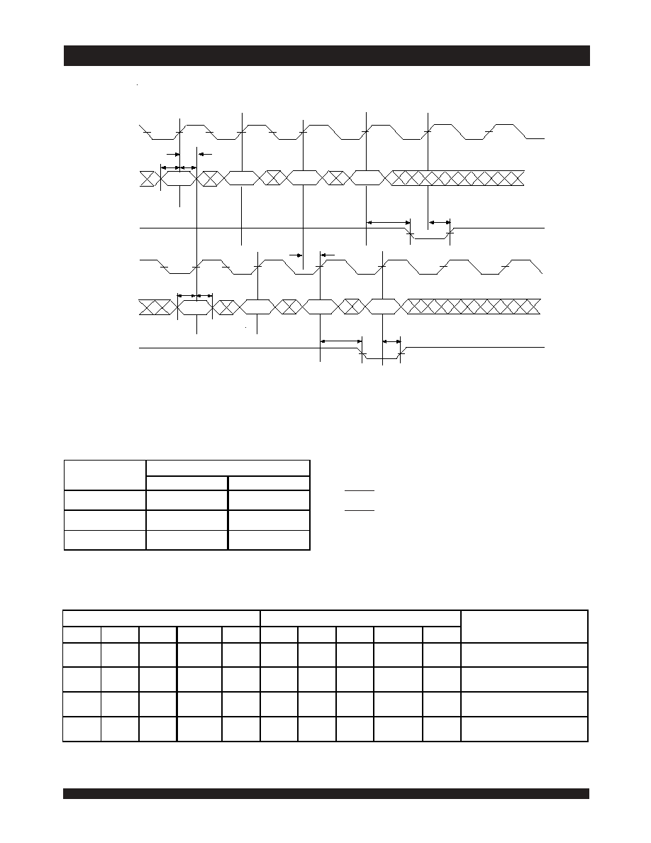
6.42
IDT70T3519/99/89S
High-Speed 2.5V 256/128/64K x 36 Dual-Port Synchronous Static RAM Industrial and Commercial Temperature Ranges
21
t
SA
t
HA
(3)
t
COLS
t
COLR
A
3
HA
t
SA
t
t
COLS
t
COLR
5666 drw 20
COL
R
COL
L
(4)
CLK
R
ADDRESS
R
A
0
A
1
A
2
t
OFS
(4)
CLK
L
ADDRESS
L
A
0
A
1
A
2
A
3
t
OFS
Waveform of Collision Timing
(1,2)
Both
Ports Writing with Left Port Clock Leading
NOTES:
1. CE
0
= V
IL
, CE
1
= V
IH
.
2. For reading port, OE is a Don't care on the Collision Detection Logic. Please refer to Truth Table IV for specific cases.
3. Leading Port Output flag might output 3t
CYC
2
+ t
COLS
after Address match.
4. Address is for internal register, not the external bus, i.e., address needs to be qualified by one of the Address counter control signals.
Collision Detection Timing
(3,4)
Cycle Time
t
OFS
(ns)
Region 1 (ns)
(1)
Region 2 (ns)
(2)
5ns
0 - 2.8
2.81 - 4.6
6ns
0 - 3.8
3.81 - 5.6
7.5ns
0 - 5.3
5.31 - 7.1
5666 tbl 13
NOTES:
1. Region 1
Both ports show collision after 2nd cycle for Addresses 0, 2, 4 etc.
2. Region 2
Leading port shows collision after 3rd cycle for addresses 0, 3, 6, etc.
while trailing port shows collision after 2nd cycle for addresses 0, 2, 4 etc.
3. All the production units are tested to midpoint of each region.
4. These ranges are based on characterization of a typical device.
Left Port
Right Port
Function
CLK
L
R/W
L
(1)
CE
L
(1)
A
17L
-A
0L
(2)
COL
L
CLK
R
R/W
R
(1)
CE
R
(1)
A
17R
-A
0R
(2)
COL
R
H
L
MATCH
H
H
L
MATCH
H
Both ports reading. Not a valid collision.
No flag output on either port.
H
L
MATCH
L
L
L
MATCH
H
Left port reading, Right port writing.
Valid collision, flag output on Left port.
L
L
MATCH
H
H
L
MATCH
L
Right port reading, Left port writing.
Valid collision, flag output on Right port.
L
L
MATCH
L
L
L
MATCH
L
Both ports writing. Valid collision. Flag
output on both ports.
5666 tbl 14
Truth Table IV -- Collision Detection Flag
NOTES:
1. CE
0 =
V
IL
and
CE
1 =
V
IH
.
R/W and CE
are synchronous with respect to the clock and need valid set-up and hold times.
2. Address is for internal register, not the external bus, i.e., address needs to be qualified by one of the Address counter control signals.

6.42
IDT70T3519/99/89S
High-Speed 2.5V 256/128/64K x 36 Dual-Port Synchronous Static RAM Industrial and Commercial Temperature Ranges
22
(3)
R/
W
Timing Waveform - Entering Sleep Mode
(1,2)
DATA
OUT
R/
W
OE
(4)
Dn
Dn+1
An+1
An
(5)
(5)
Timing Waveform - Exiting Sleep Mode
(1,2)
NOTES:
1. CE
1 =
V
IH.
2. All timing is same for Left and Right ports.
3. CE
0
has to be deactivated (CE
0
= V
IH
) three cycles prior to asserting ZZ (ZZx = V
IH
) and held for two cycles after asserting ZZ (ZZx = V
IH
).
4. CE
0
has to be deactivated (CE
0
= V
IH
) one cycle prior to de-asserting ZZ
(ZZx = V
IL
) and held for three cycles after de-asserting ZZ (ZZx = V
IL
).
5. The device must be in Read Mode (R/W High) when exiting sleep mode. Outputs are active but data is not valid until the following cycle.

6.42
IDT70T3519/99/89S
High-Speed 2.5V 256/128/64K x 36 Dual-Port Synchronous Static RAM Industrial and Commercial Temperature Ranges
23
Functional Description
The IDT70T3519/99/89 provides a true synchronous Dual-Port Static
RAM interface. Registered inputs provide minimal set-up and hold times
on address, data, and all critical control inputs. All internal registers are
clocked on the rising edge of the clock signal, however, the self-timed
internal write pulse width is independent of the cycle time.
An asynchronous output enable is provided to ease asyn-
chronous bus interfacing. Counter enable inputs are also provided to stall
the operation of the address counters for fast interleaved
memory applications.
A HIGH on CE
0
or a LOW on CE
1
for one clock cycle will power down
the internal circuitry to reduce static power consumption. Multiple chip
enables allow easier banking of multiple IDT70T3519/99/89s for depth
expansion configurations. Two cycles are required with CE
0
LOW and
CE
1
HIGH to re-activate the outputs.
Interrupts
If the user chooses the interrupt function, a memory location (mail
box or message center) is assigned to each port. The left port interrupt
flag (INT
L
) is asserted when the right port writes to memory location
3FFFE (HEX), where a write is defined as CE
R
= R/W
R
= V
IL
per the
Truth Table. The left port clears the interrupt through access of
address location 3FFFE when CE
L
= V
IL
and R/WL = V
IH
. Likewise, the
right port interrupt flag (INT
R
) is asserted when the left
port writes to memory location 3FFFF (HEX) and to clear the interrupt
flag (INT
R
), the right port must read the memory location 3FFFF (1FFFF
or 1FFFE for IDT70T3599 and FFFF or FFFE for IDT70T3589). The
message (36 bits) at 3FFFE or 3FFFF (1FFFF or 1FFFE for IDT70T3599
and FFFF or FFFE for IDT70T3589) is user-defined since it is an
addressable SRAM location. If the interrupt function is not used, address
locations 3FFFE and 3FFFF (1FFFF or 1FFFE for IDT70T3599 and
FFFF or FFFE for IDT70T3589) are not used as mail boxes, but as part
of the random access memory. Refer to Truth Table III for the interrupt
operation.
Collision Detection
Sleep Mode
The IDT70T3519/99/89 is equipped with an optional sleep or low
power mode on both ports. The sleep mode pin on both ports is
asynchronous and active high. During normal operation, the ZZ pin is
pulled low. When ZZ is pulled high, the port will enter sleep mode where
it will meet lowest possible power conditions. The sleep mode timing
diagram shows the modes of operation: Normal Operation, No Read/Write
Allowed and Sleep Mode.
For normal operation all inputs must meet setup and hold times prior
to sleep and after recovering from sleep. Clocks must also meet cycle high
and low times during these periods. Three cycles prior to asserting ZZ
(ZZx = V
IH
) and three cycles after de-asserting ZZ (ZZx = V
IL
), the device
must be disabled via the chip enable pins. If a write or read operation occurs
during these periods, the memory array may be corrupted. Validity of data
out from the RAM cannot be guaranteed immediately after ZZ is asserted
(prior to being in sleep). When exiting sleep mode, the device must be in
Read mode (R/Wx = V
IH
)when chip enable is asserted, and the chip
enable must be valid for one full cycle before a read will result in the output
of valid data.
During sleep mode the RAM automatically deselects itself. The RAM
disconnects its internal clock buffer. The external clock may continue to run
without impacting the RAMs sleep current (I
ZZ
). All outputs will remain in
high-Z state while in sleep mode. All inputs are allowed to toggle. The RAM
will not be selected and will not perform any reads or writes.
Collision is defined as an overlap in access between the two ports
resulting in the potential for either reading or writing incorrect data to a
specific address. For the specific cases: (a) Both ports reading - no
data is corrupted, lost, or incorrectly output, so no collision flag is output
on either port. (b) One port writing, the other port reading - the end
result of the write will still be valid. However, the reading port might
capture data that is in a state of transition and hence the reading port's
collision flag is output. (c) Both ports writing - there is a risk that the two
ports will interfere with each other, and the data stored in memory will
not be a valid write from either port (it may essentially be a random
combination of the two). Therefore, the collision flag is output on both
ports. Please refer to Truth Table IV for all of the above cases.
The alert flag
(COL
X
) is asserted on the 2nd or 3rd rising clock
edge of the affected port following the collision, and remains low for
one cycle. Please refer to Collision Detection Timing table on Page 21.
During that next cycle, the internal arbitration is engaged in resetting
the alert flag (this avoids a specific requirement on the part of the user
to reset the alert flag). If two collisions occur on subsequent clock
cycles, the second collision may not generate the appropriate alert
Collision detection on the IDT70T3519/99/89 represents a
significant advance in functionality over current sync multi-ports, which
have no such capability. In addition to this functionality the
IDT70T3519/99/89 sustains the key features of bandwidth and
flexibility. The collision detection function is very useful in the case of
bursting data, or a string of accesses made to sequential addresses, in
that it indicates a problem within the burst, giving the user the option of
either repeating the burst or continuing to watch the alert flag to see
whether the number of collisions increases above an acceptable
threshold value. Offering this function on chip also allows users to
reduce their need for arbitration circuits, typically done in CPLD's or
FPGA's. This reduces board space and design complexity, and gives
the user more flexibility in developing a solution.
flag. A third collision will generate the alert flag as appropriate. In the
event that a user initiates a burst access on both ports with the same
starting address on both ports and one or both ports writing during
each access (i.e., imposes a long string of collisions on contiguous
clock cycles), the alert flag will be asserted and cleared every other
cycle. Please refer to the Collision Detection timing waveform on Page
21.
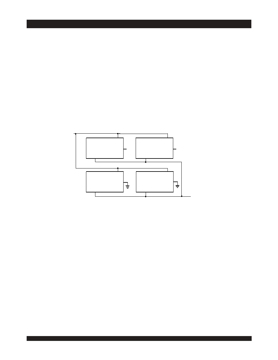
6.42
IDT70T3519/99/89S
High-Speed 2.5V 256/128/64K x 36 Dual-Port Synchronous Static RAM Industrial and Commercial Temperature Ranges
24
Figure 4. Depth and Width Expansion with IDT70T3519/99/89
Depth and Width Expansion
The IDT70T3519/99/89 features dual chip enables (refer to Truth
Table I) in order to facilitate rapid and simple depth expansion with no
requirements for external logic. Figure 4 illustrates how to control the
various chip enables in order to expand two devices in depth.
The IDT70T3519/99/89 can also be used in applications requiring
expanded width, as indicated in Figure 4. Through combining the control
signals, the devices can be grouped as necessary to accommodate
applications needing 72-bits or wider.
NOTE:
1. A
18
is for IDT70T3519, A
17
is for IDT70T3599, A
16
is for IDT70T3589.
5666 drw 23
IDT70T3519/99/89
CE
0
CE
1
CE
1
CE
0
CE
0
CE
1
A
18
/A
17
/A
16
CE
1
CE
0
V
DD
V
DD
IDT70T3519/99/89
IDT70T3519/99/89
IDT70T3519/99/89
Control Inputs
Control Inputs
Control Inputs
Control Inputs
BE
,
R/
W
,
OE
,
CLK,
ADS
,
REPEAT
,
CNTEN
,
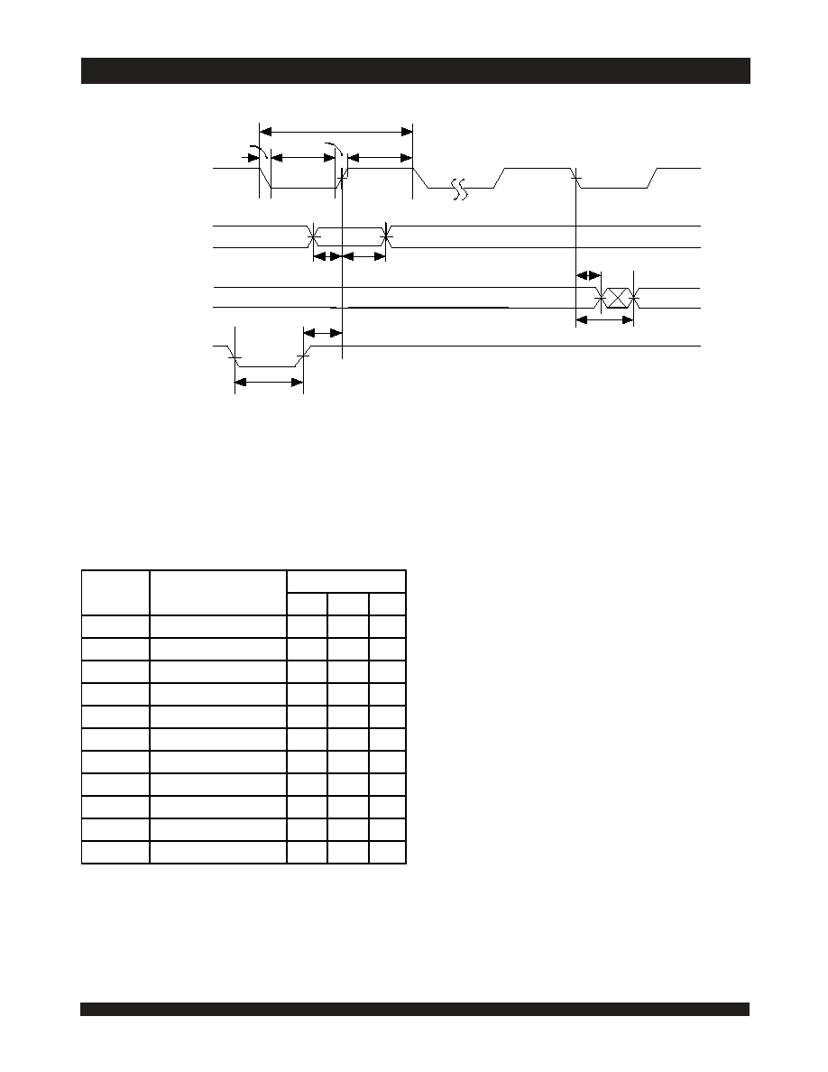
6.42
IDT70T3519/99/89S
High-Speed 2.5V 256/128/64K x 36 Dual-Port Synchronous Static RAM Industrial and Commercial Temperature Ranges
25
JTAG AC Electrical
Characteristics
(1,2,3,4)
70T3519/99/89
Symbol
Parameter
Min.
Max.
Units
t
JCYC
JTAG Clock Input Period
100
____
ns
t
JCH
JTAG Clock HIGH
40
____
ns
t
JCL
JTAG Clock Low
40
____
ns
t
JR
JTAG Clock Rise Time
____
3
(1)
ns
t
JF
JTAG Clock Fall Time
____
3
(1)
ns
t
JRST
JTAG Reset
50
____
ns
t
JRSR
JTAG Reset Recovery
50
____
ns
t
JCD
JTAG Data Output
____
25
ns
t
JDC
JTAG Data Output Hold
0
____
ns
t
JS
JTAG Setup
15
____
ns
t
JH
JTAG Hold
15
____
ns
5666 tbl 15
NOTES:
1. Guaranteed by design.
2. 30pF loading on external output signals.
3. Refer to AC Electrical Test Conditions stated earlier in this document.
4. JTAG operations occur at one speed (10MHz). The base device may run at
any speed specified in this datasheet.
JTAG Timing Specifications
TCK
Device Inputs
(1)
/
TDI/TMS
Device Outputs
(2)
/
TDO
TRST
t
JCD
t
JDC
t
JRST
t
JS
t
JH
t
JCYC
t
JRSR
t
JF
t
JCL
t
JR
t
JCH
5666 drw 24
,
Figure 5. Standard JTAG Timing
NOTES:
1. Device inputs = All device inputs except TDI, TMS, and TRST.
2. Device outputs = All device outputs except TDO.

6.42
IDT70T3519/99/89S
High-Speed 2.5V 256/128/64K x 36 Dual-Port Synchronous Static RAM Industrial and Commercial Temperature Ranges
26
Identification Register Definitions
Instruction Field
Value
Description
Revision Number (31:28)
0x0
Reserved for version number
IDT Device ID (27:12)
0x330
(1)
Defines IDT part number
IDT JEDEC ID (11:1)
0x33
Allows unique identification of device vendor as IDT
ID Register Indicator Bit (Bit 0)
1
Indicates the presence of an ID register
5666 tbl 16
NOTE:
1. Device ID for IDT70T3599 is 0x331. Device ID for IDT70T3589 is 0x332.
Scan Register Sizes
Register Name
Bit Size
Instruction (IR)
4
Bypass (BYR)
1
Identification (IDR)
32
Boundary Scan (BSR)
Note (3)
5666 tbl 17
System Interface Parameters
Instruction
Code
Description
EXTEST
0000
Forces contents of the boundary scan cells onto the device outputs
(1)
.
Places the boundary scan register (BSR) between TDI and TDO.
BYPASS
1111
Places the bypass register (BYR) between TDI and TDO.
IDCODE
0010
Loads the ID register (IDR) with the vendor ID code and places the
register between TDI and TDO.
HIGHZ
0100
Places the bypass register (BYR) between TDI and TDO. Forces all
device output drivers to a High-Z state except COLx & INTx outputs.
CLAMP
0011
Uses BYR. Forces contents of the boundary scan cells onto the device
outputs. Places the bypass register (BYR) between TDI and TDO.
SAMPLE/PRELOAD
0001
Places the boundary scan register (BSR) between TDI and TDO.
SAMPLE allows data from device inputs
(2)
to be captured in the
boundary scan cells and shifted serially through TDO. PRELOAD allows
data to be input serially into the boundary scan cells via the TDI.
RESERVED
0101, 0111, 1000, 1001,
1010, 1011, 1100
Several combinations are reserved. Do not use codes other than those
identified above.
PRIVATE
0110,1110,1101
For internal use only.
5666 tbl 18
NOTES:
1. Device outputs = All device outputs except TDO.
2. Device inputs = All device inputs except TDI, TMS, and TRST.
3. The Boundary Scan Descriptive Language (BSDL) file for this device is available on the IDT website (www.idt.com), or by contacting your local
IDT sales representative.

6.42
IDT70T3519/99/89S
High-Speed 2.5V 256/128/64K x 36 Dual-Port Synchronous Static RAM Industrial and Commercial Temperature Ranges
27
Ordering Information
A
Power
999
Speed
A
Package
A
Process/
Temperature
Range
XXXXX
Device
Type
Blank
I
BC
DR
BF
200
166
133
70T3519
70T3599
70T3589
S
Commercial (0∞C to +70∞C)
Industrial (-40∞C to +85∞C)
256-pin BGA (BC-256)
208-pin PQFP (DR-208)
208-pin fpBGA (BF-208)
9Mbit (256K x 36)
2.5V Synchronous Dual-Port RAM
4Mbit (128K x 36)
2.5V Synchronous Dual-Port RAM
2Mbit (64K x 36)
2.5V Synchronous Dual-Port RAM
Standard Power
Speed in Megahertz
Commercial Only
(2)
Commercial & Industrial
(1)
Commercial & Industrial
5666 drw 25
IDT
NOTES:
1. 166MHz I-Temp is not available in the BF-208 package.
2. 200Mhz is not available in the BF-208 and DR-208 packages.
IDT Clock Solution for IDT70T3519/99/89 Dual-Port
IDT Dual-Port
Part Number
Dual-Port I/O Specitications
Clock Specifications
IDT
PLL
Clock Device
IDT
Non-PLL
Clock Device
Voltage
I/O
Input
Capacitance
Input Duty
Cycle
Requirement
Maximum
Frequency
Jitter
Tolerance
70T3519/99/89
2.5
LVTTL
8pF
40%
200
75ps
5T2010
5T9010
5T905, 5T9050
5T907, 5T9070
5666 tbl 19

6.42
IDT70T3519/99/89S
High-Speed 2.5V 256/128/64K x 36 Dual-Port Synchronous Static RAM Industrial and Commercial Temperature Ranges
28
The IDT logo is a registered trademark of Integrated Device Technology, Inc.
CORPORATE HEADQUARTERS
for SALES:
for Tech Support:
2975 Stender Way
800-345-7015 or 408-727-5166
831-754-4613
Santa Clara, CA 95054
fax: 408-492-8674
DualPortHelp@idt.com
www.idt.com
Datasheet Document History:
01/23/03:
Initial Datasheet
01/30/03:
Page 1 Corrected 208-pin package from TQFP to PQFP
04/25/03:
Page 11 Added Capacitance Derating drawing
Page 12 Changed t
INS
and t
INR
specs in AC Electrical Characteristics table
11/11/03:
Page 10 Updated power numbers in DC Electrical Characteristics table
Page 12 Added t
OFS
symbol and parameter to AC Electrical Characteristics table
Page 21 Updated Collision Timing waveform
Page 22 Added Collision DetectionTiming table and footnotes
Page 26 Updated HIGHZ function in System Interface Parameters table
Page 27 Added IDT Clock Solution table
03/30/04:
Page 22 & 23 Clarified Sleep Mode Text and Waveforms
Page 1 & 27 Removed Preliminary status
04/22/04:
Page 6 Added another sentence to footnote 4 to recommend that boundary scan not be operated during sleep mode