Äîêóìåíòàöèÿ è îïèñàíèÿ www.docs.chipfind.ru
©2000 Integrated Device Technology, Inc.
6.01
1
JANUARY 2001
DSC 3603/7
Features:
x
True Dual-Ported memory cells which allow simultaneous
access of the same memory location
x
High-speed access
Industrial: 35ns (max.)
Commercial: 15/20/25/35/55ns (max.)
x
Low-power operation
IDT70V27S
Active: 500mW (typ.)
Standby: 3.3mW (typ.)
IDT70V27L
Active: 500mW (typ.)
Standby: 660
µ
W (typ.)
x
Separate upper-byte and lower-byte control for bus
matching capability
x
Dual chip enables allow for depth expansion without
external logic
IDT70V27S/L
x
IDT70V27 easily expands data bus width to 32 bits or more
using the Master/Slave select when cascading more than
one device
x
M/
S = V
IH
for
BUSY output flag on Master,
M/
S = V
IL
for
BUSY input on Slave
x
Busy and Interrupt Flags
x
On-chip port arbitration logic
x
Full on-chip hardware support of semaphore signaling
between ports
x
Fully asynchronous operation from either port
x
LVTTL-compatible, single 3.3V (±0.3V) power supply
x
Available in 100-pin Thin Quad Flatpack (TQFP), 108-pin
Ceramic Pin Grid Array (PGA), and 144-pin Fine Pitch BGA
(fpBGA)
x
Industrial temperature range (-40°C to +85°C) is available
for selected speeds
I/O
Control
Address
Decoder
32Kx16
MEMORY
ARRAY
70V27
ARBITRATION
INTERRUPT
SEMAPHORE
LOGIC
CE
0L
OE
L
R/
W
L
A
14L
A
0L
A
14L
A
0L
SEM
L
INT
L
(2)
BUSY
L
(1,2)
LB
L
CE
0L
OE
L
UB
L
I/O
Control
Address
Decoder
CE
0R
OE
R
R/
W
R
A
14R
A
0R
A
14R
A
0R
SEM
R
INT
R
(2)
BUSY
R
(1,2)
LB
R
R/
W
R
OE
R
UB
R
M/
S
(2)
CE
1L
CE
0R
CE
1R
3603 drw 01
I/O
0-7L
CE
1R
CE
1L
I/O
8-15L
I/O
0-7R
I/O
8-15R
R/
W
L
NOTES:
1)
BUSY is an input as a Slave (M/S=V
IL
) and an output as a Master (M/
S=V
IH
).
2)
BUSY and INT are non-tri-state totem-pole outputs (push-pull).
HIGH-SPEED 3.3V
32K x 16 DUAL-PORT
STATIC RAM
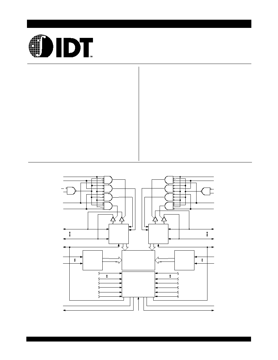
Functional Block Diagram
Commercial and Industrial Temperature Range
IDT 70V27S/L
High-Speed 3.3V 32K x 16 Dual-Port Static RAM
2
Description:
The IDT70V27 is a high-speed 32K x 16 Dual-Port Static RAM,
designed to be used as a stand-alone 512K-bit Dual-Port RAM or as a
combination MASTER/SLAVE Dual-Port RAM for 32-bit and wider word
systems. Using the IDT MASTER/SLAVE Dual-Port RAM approach in 32-
bit or wider memory system applications results in full-speed, error-free
operation without the need for additional discrete logic.
The device provides two independent ports with separate control,
address, and I/O pins that permit independent, asynchronous access for
reads or writes to any location in memory. An automatic power down
feature controlled by the chip enables (
CE
0
and
CE
1
) permits the on-chip
circuitry of each port to enter a very low standby power mode.
Fabricated using IDT's CMOS high-performance technology,
these devices typically operate on only 500mW of power. The IDT70V27
is packaged in a 100-pin Thin Quad Flatpack (TQFP), a 108-pin ceramic
Pin Grid Array (PGA), and a 144-pin Fine Pitch BGA (fp BGA).
Pin Configurations
(1,2,3)
NOTES:
1. All V
CC
pins must be connected to power supply.
2. All GND pins must be connected to ground supply.
3. Package body is approximately 14mm x 14mm x 1.4mm.
4. This package code is used to reference the package diagram.
5. This text does not indicate orientation of the actual part-marking.
INDEX
1
2
3
4
5
6
7
8
9
10
11
12
13
14
15
16
17
18
19
20
21
22
23
24
25
75
74
73
72
71
70
69
68
67
66
65
64
63
62
61
60
59
58
57
56
55
54
53
52
51
26 27 28 29 30 31 32 33 34 35 36 37 38 39 40 41 42 43 44 45 46 47 48 49 50
100 99 98 97 96 95 94 93 92 91 90 89 88 87 86 85 84 83 82 81 80 79 78 77 76
IDT70V27PF
PN100-1
(4)
100-PIN TQFP
TOP VIEW
(5)
GND
OE
R
R/
W
R
SEM
R
CE
1R
CE
0R
NC
NC
GND
A
12R
A
13R
A
11R
A
10R
A
9R
A
14R
NC
I/O
10R
I/O
11R
I/O
12R
I/O
13R
I/O
14R
I/O
15R
GND
UB
R
LB
R
3603 drw 02
I/O
15L
GND
OE
L
R/
W
L
SEM
L
CE
1L
CE
0L
Vcc
NC
A
14L
A
13L
NC
NC
A
12L
A
11L
A
10L
A
9L
I/O
10L
I/O
11L
I/O
12L
I/O
13L
I/O
14L
UB
L
LB
L
GND
I
/
O
5
R
I
/
O
4
R
I
/
O
3
R
I
/
O
2
R
I
/
O
0
R
I
/
O
0
L
G
N
D
I
/
O
2
L
I
/
O
4
L
I
/
O
5
L
I
/
O
6
L
I
/
O
7
L
I
/
O
3
L
I
/
O
1
R
I
/
O
7
R
N
C
I
/
O
8
R
I
/
O
9
R
I
/
O
8
L
I
/
O
9
L
I
/
O
6
R
A
7
R
A
8
L
A
7
L
A
6
R
A
5
R
A
4
R
A
3
R
A
2
R
A
1
R
A
0
R
I
N
T
R
B
U
S
Y
R
M
/
S
B
U
S
Y
L
I
N
T
L
N
C
A
0
L
A
2
L
A
3
L
A
5
L
A
6
L
A
1
L
A
4
L
A
8
R
G
N
D
V
c
c
I
/
O
1
L
V
c
c
G
N
D

Commercial and Industrial Temperature Range
IDT 70V27S/L
High-Speed 3.3V 32K x 16 Dual-Port Static RAM
3
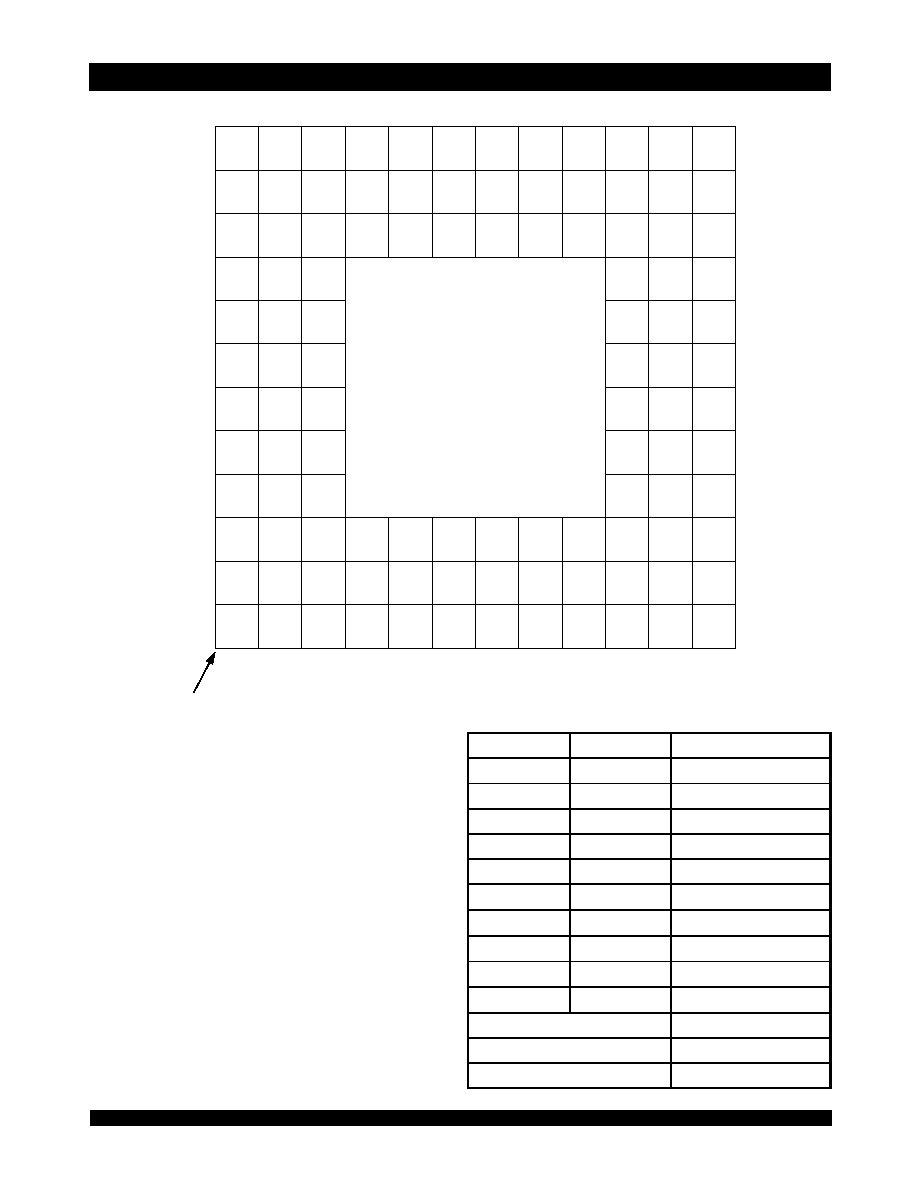
Pin Configurations
(1,2,3)
(con't.)
NOTES:
1. All V
CC
pins must be connected to power supply.
2. All GND pins must be connected to ground supply.
3. Package body is approximately 12mm x 12mm x 1.4mm.
4. This package code is used to reference the package diagram.
5. This text does not indicate orientation of the actual part-marking.
3603 drw 02a
IDT70V27BF
BF144-1
(4)
144-Pin fpBGA
Top View
(5)
M/
S
BUSY
L
A
2L
A
4L
A
7L
NC
NC
A
11L
I/O
3R
V
CC
I/O
2R
GND
I/O
0R
GND
I/O
0L
I/O
3L
NC
I/O
6L
I/O
5L
V
CC
NC
NC
NC
NC
LB
R
CE
0R
SEM
R
GND
I/O
14R
GND
NC
GND
R/
W
R
OE
R
I/O1
5R
I/O
12R
NC
GND
CE
1R
NC
I/O
10R
NC
NC
NC
A
12L
A
13L
NC
NC
UB
L
CE
0L
V
CC
V
CC
NC
R/
W
L
CE
1L
I/O
15L
NC
NC
NC
OE
L
I/O
14L
NC
A
9L
I/O
10L
I/0
13L
A
6L
NC
NC
I/O
11R
NC
I/O
8R
NC
I/O
6R
NC
I/O
2L
I/O
4L
I/O
5R
NC
NC
NC
I/O
4R
I/O
7R
NC
UB
R
NC
NC
I/O
13R
A1
NC
A2
NC
A3
A
8L
A4
A
5L
A5
A
1L
A6
INT
L
A7
GND
A8
BUSY
R
A9
A
1R
NC
A
10L
A
14L
A10
A
5R
A11
NC
A12
NC
A13
NC
LB
L
SEM
L
V
CC
NC
GND
I/O
12L
I/O
11L
I/O
9L
NC
NC
I/O
8L
I/O
7L
NC
I/O
1L
V
CC
I/O
1R
NC
V
CC
NC
NC
NC
B1
B2
B3
B4
B5
B6
B7
B8
B9
B10
B11
B12
B13
C1
C2
C3
C4
C5
C6
C7
C8
C9
C10
C11
C12
C13
D1
D2
D3
D4
D5
D6
D7
D8
D9
D10
D11
D12
D13
E1
E2
E3
E4
E10
E11
E12
E13
F1
F2
F3
F4
F10
F11
F12
F13
G1
G2
G3
G4
G10
G11
G12
G13
H1
H2
H3
H4
H10
H11
H12
H13
J1
J2
J3
J4
J10
J11
J12
J13
K1
K2
K3
K4
K5
K6
K7
K8
K9
K10
K11
K12
K13
L1
L2
L3
L4
L5
L6
L7
L8
L9
L10
L11
L12
L13
M1
M2
M3
M4
M5
M6
M7
M8
M9
M10
M11
M12
M13
N1
N2
N3
N4
N5
N6
N7
N8
N9
N10
N11
N12
N13
INT
R
A
2R
A
6R
A
3L
NC
NC
NC
A
3R
A
7R
A
9R
A
10R
A
11R
A
4R
A
8R
A
12R
A
13R
A
14R
A
0R
A
0L
I/O
9R
,
Commercial and Industrial Temperature Range
IDT 70V27S/L
High-Speed 3.3V 32K x 16 Dual-Port Static RAM
4
Pin Configurations
(1,2,3)
(con't.)
3603 drw 03
80
77
74
72
69
68
65
63
60
83
78
76
73
70
67
64
61
59
84
56
86
87
88
90
91
92
94
95
97
96
100
99
103
101
105
104
2
1
5
4
7
8
10
12
13
17
16
21
19
25
22
28
24
32
31
34
35
37
39
40
44
43
48
46
52
49
55
51
IDT70V27G
G108-1
(4)
108-PIN PGA
TOP VIEW
(5)
A
B
C
D
E
F
G
H
J
K
L
M
81
57
54
53
82
79
75
71
66
62
58
50
33
36
38
41
42
45
47
3
6
9
11
14
15
18
20
23
29
30
26
27
85
89
93
98
102
106
107
108
12
11
10
09
08
07
06
05
04
03
02
01
INDEX
GND
OE
R
R/
W
R
SEM
R
CE
1R
CE
0R
NC
NC
GND
A
12R
A
13R
A
11R
A
10R
A
9R
GND
OE
L
R/
W
L
SEM
L
CE
1L
CE
0L
Vcc
NC
A
14L
A
13L
NC
NC
A
12L
A
11L
A
10L
A
9L
I/O
6R
I/O
5R
I/O
4R
I/O
3R
I/O
2R
I/O
0R
GND
Vcc
I/O
0L
I/O
1L
GND
I/O
2L
I/O
4L
I/O
5L
I/O
6L
I/O
7L
I/O
3L
I/O
1R
I/O
7R
NC
I/O
8R
I/O
9R
I/O
8L
I/O
9L
Vcc
A
6R
A
5R
A
4R
A
3R
A
2R
A
1R
A
0R
INT
R
BUSY
R
M/
S
BUSY
L
INT
L
NC
A
0L
GND
A
2L
A
3L
A
5L
A
6L
A
1L
A
4L
A
8R
A
7R
A
8L
A
7L
A
14R
NC
I/O
10R
I/O
11R
I/O
12R
I/O
13R
I/O
14R
I/O
15R
I/O
10L
I/O
11L
I/O
12L
I/O
13L
I/O
14L
GND
UB
R
LB
R
UB
L
LB
L
GND
NC
NC
NC
NC
NC
NC
NC
NC
I/O
15L
Left Port
Right Port
Names
CE
0L
, CE
1L
CE
0R
, CE
1R
Chip Enable
R/W
L
R/W
R
Read/Write Enable
OE
L
OE
R
Output Enable
A
0L
- A
14L
A
0R
- A
14R
Address
I/O
0L
- I/O
15L
I/O
0R
- I/O
15R
Data Input/Output
SEM
L
SEM
R
Semaphore Enable
UB
L
UB
R
Upper Byte Select
LB
L
LB
R
Lower Byte Select
INT
L
INT
R
Interrupt Flag
BUSY
L
BUSY
R
Busy Flag
M/S
Master or Slave Select
V
CC
Power
GND
Ground
3603 tbl 01
Pin Names
NOTES:
1. All V
CC
pins must be connected to power supply.
2. All GND pins must be connected to ground supply.
3. Package body is approximately 1.21in x 1.21in x .16in.
4. This package code is used to reference the package diagram.
5. This text does not indicate orientation of the actual part-marking.
Commercial and Industrial Temperature Range
IDT 70V27S/L
High-Speed 3.3V 32K x 16 Dual-Port Static RAM
5
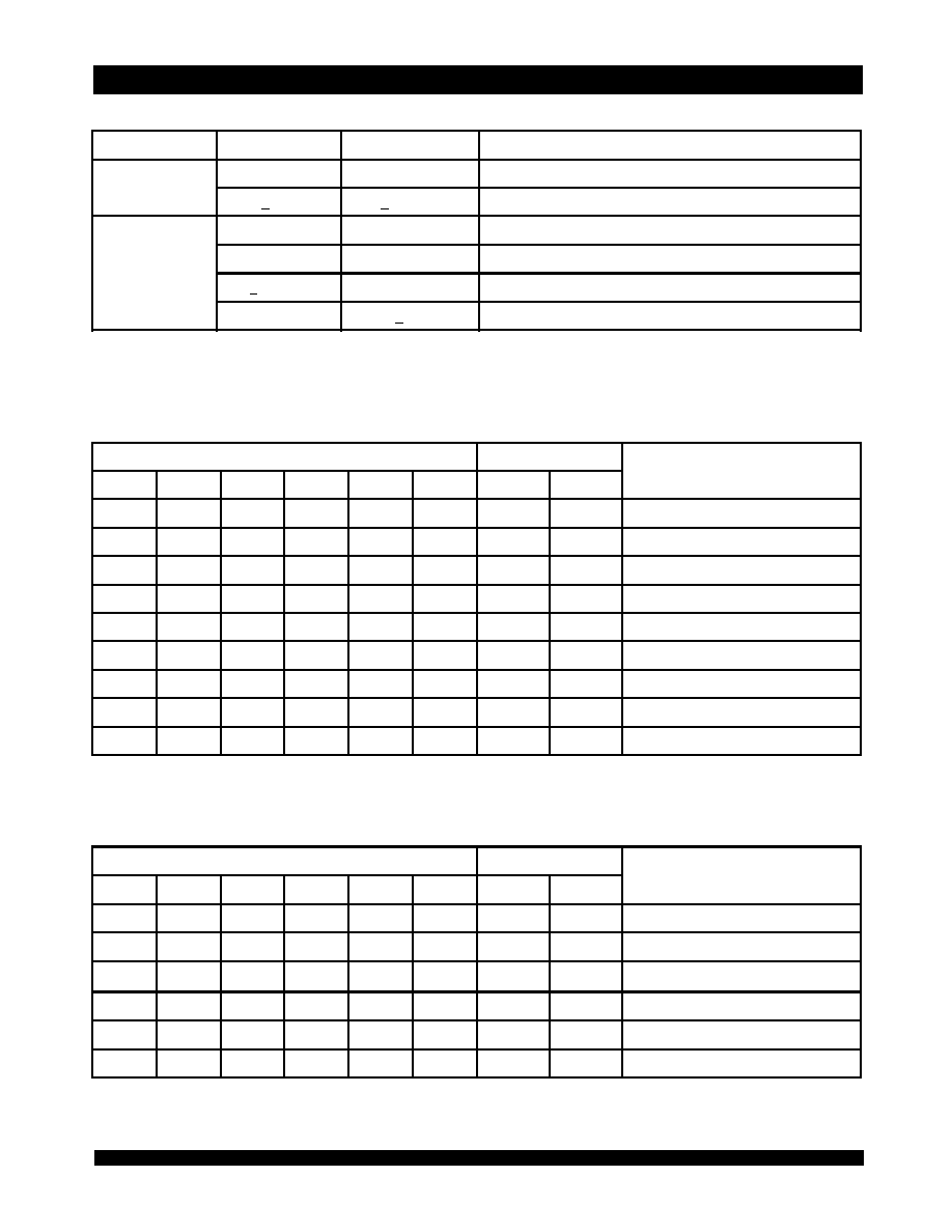
Truth Table II Non-Contention Read/Write Control
NOTES:
1. Chip Enable references are shown above with the actual
CE
0
and CE
1
levels,
CE is a reference only.
2. Port "A" and "B" references are located where
CE is used.
3. "H" = V
IH
and "L" = V
IL
Truth Table I Chip Enable
(1,2,3)
Truth Table III Semaphore Read/Write Control
NOTES:
1. A
0L
-- A
14L
A
0R
-- A
14R.
2. Refer to Chip Enable Truth Table.
NOTES:
1. There are eight semaphore flags written to I/O
0
and read from all the I/Os (I/O
0
-I/O
15
). These eight semaphore flags are addressed by A
0
-A
2
.
2. Refer to Chip Enable Truth Table.
CE
CE
0
CE
1
Mode
L
V
IL
V
IH
Port Selected (TTL Active)
< 0.2V
>V
CC
-0.2V
Port Selected (CMOS Active)
H
V
IH
X
Port Deselected (TTL Inactive)
X
V
IL
Port Deselected (TTL Inactive)
>V
CC
-0.2V
X
Port Deselected (CMOS Inactive)
X
<0.2V
Port Deselected (CMOS Inactive)
3603 tbl 02
Inputs
(1)
Outputs
Mode
CE
(2)
R/
W
OE
UB
LB
SEM
I/O
8-15
I/O
0-7
H
X
X
X
X
H
High-Z
High-Z
Deselected: Power-Down
X
X
X
H
H
H
High-Z
High-Z
Both Bytes Deselected
L
L
X
L
H
H
DATA
IN
High-Z
Write to Upper Byte Only
L
L
X
H
L
H
High-Z
DATA
IN
Write to Lower Byte Only
L
L
X
L
L
H
DATA
IN
DATA
IN
Write to Both Bytes
L
H
L
L
H
H
DATA
OUT
High-Z
Read Upper Byte Only
L
H
L
H
L
H
High-Z
DATA
OUT
Read Lower Byte Only
L
H
L
L
L
H
DATA
OUT
DATA
OUT
Read Both Bytes
X
X
H
X
X
X
High-Z
High-Z
Outputs Disabled
3603 tbl 03
Inputs
(1)
Outputs
Mode
CE
(2)
R/
W
OE
UB
LB
SEM
I/O
8-15
I/O
0-7
H
H
L
X
X
L
DATA
OUT
DATA
OUT
Read Data in Semaphore Flag
X
H
L
H
H
L
DATA
OUT
DATA
OUT
Read Data in Semaphore Flag
H
X
X
X
L
DATA
IN
DATA
IN
Write I/O
0
into Semaphore Flag
X
X
H
H
L
DATA
IN
DATA
IN
Write I/O
0
into Semaphore Flag
L
X
X
L
X
L
______
______
Not Allowed
L
X
X
X
L
L
______
______
Not Allowed
3603 tbl 04