1
©2004 Integrated Device Technology, Inc.
JUNE 2004
DSC-2692/16
HIGH SPEED
2K x 8 DUAL PORT
STATIC RAM
IDT7132SA/LA
IDT7142SA/LA
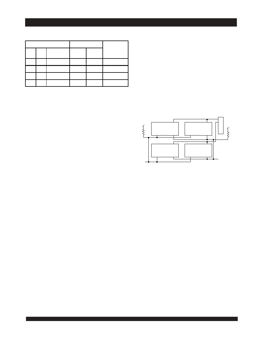
Functional Block Diagram
Features
High-speed access
≠ Commercial: 20/25/35/55/100ns (max.)
≠ Industrial: 25ns (max.)
≠ Military: 25/35/55/100ns (max.)
Low-power operation
≠ IDT7132/42SA
Active: 325mW (typ.)
Standby: 5mW (typ.)
≠ IDT7132/42LA
Active: 325mW (typ.)
Standby: 1mW (typ.)
NOTES:
1. IDT7132 (MASTER): BUSY is open drain output and requires pullup resistor of 270
.
IDT7142 (SLAVE): BUSY is input.
2. Open drain output: requires pullup resistor of 270
.
MASTER IDT7132 easily expands data bus width to 16-or-more
bits using SLAVE IDT7142
On-chip port arbitration logic (IDT7132 only)
BUSY
output flag on IDT7132; BUSY input on IDT7142
Battery backup operation --2V data retention (LA only)
TTL-compatible, single 5V ±10% power supply
Available in 48-pin DIP, LCC and Flatpack, and 52-pin PLCC
packages
Military product compliant to MIL-PRF-38535 QML
Industrial temperature range (≠40∞C to +85∞C) is available for
selected speeds
OE
L
CE
L
R/W
L
I/O
OL-
I/O
7L
BUSY
L
(1,2)
A
10L
A
0L
CE
L
OE
L
R/
W
L
CE
R
OE
R
R/
W
R
OE
R
CE
R
R/
W
R
I/O
OR-
I/O
7R
BUSY
R
(1,2)
A
10R
A
0R
I/O
Control
I/O
Control
Address
Decoder
Address
Decoder
MEMORY
ARRAY
ARBITRATION
LOGIC
2692 drw 01
m
11
11
2
IDT7132SA/LA and IDT 7142SA/LA
High Speed 2K x 8 Dual Port Static RAM Military, Industrial and Commercial Temperature Ranges
Pin Configurations
(1,2,3)
NOTES:
1. All V
CC
pins must be connected to the power supply.
2. All GND pins must be connected to the ground supply.
3. P48-1 package body is approximately .55 in x 2.43 in x .18 in.
C48-2 package body is approximately .62 in x 2.43 in x .15 in.
L48-1 package body is approximately .57 in x .57 in x .68 in.
F48-1 package body is approximately .75 in x .75 in x .11 in.
4. This package code is used to reference the package diagram.
5. This text does not indicate orientation of the actual part-marking.
Description
The IDT7132/IDT7142 are high-speed 2K x 8 Dual-Port Static RAMs.
The IDT7132 is designed to be used as a stand-alone 8-bit Dual-Port RAM
or as a "MASTER" Dual-Port RAM together with the IDT7142 "SLAVE"
Dual-Port in 16-bit-or-more word width systems. Using the IDT MASTER/
SLAVE Dual-Port RAM approach in 16-or-more-bit memory system
applications results in full-speed, error-free operation without the need for
additional discrete logic.
Both devices provide two independent ports with separate control,
address, and l/O pins that permit independent, asynchronous access for
reads or writes to any location in memory. An automatic power down
feature, controlled by CE permits the on-chip circuitry of each port to enter
a very low standby power mode.
Fabricated using IDT's CMOS high-performance technology, these
devices typically operate on only 325mW of power. Low-power (LA)
versions offer battery backup data retention capability, with each Dual-
Port typically consuming 200µW from a 2V battery.
The IDT7132/7142 devices are packaged in a 48-pin sidebraze or
plastic DIPs, 48-pin LCCs, 52-pin PLCCs, and 48-lead flatpacks.
Military grade product is manufactured in compliance with the latest
revision of MIL-PRF-38535 QML, making it ideally suited to military
temperature applications demanding the highest level of performance
and reliability.
24
23
22
21
20
19
18
17
16
15
14
13
12
11
10
9
8
7
6
5
4
3
2
1
48
47
46
45
44
43
42
41
40
39
38
37
36
35
34
33
32
31
30
29
28
27
26
25
IDT7132/
7142
P or C
P48-1
(4)
&
C48-2
(4)
48-Pin
DIP
Top
View
(5)
2692 drw 02
GND
I/O
6R
I/O
5R
I/O
4R
I/O
3R
I/O
2R
I/O
1R
I/O
0R
I/O
7L
I/O
6L
I/O
5L
I/O
4L
CE
R
CE
L
OE
L
A
0L
BUSY
L
R/
W
L
R/
W
R
BUSY
R
V
CC
OE
R
A
0R
A
1R
A
2R
A
3R
A
4R
A
5R
A
6R
A
7R
A
8R
A
9R
I/O
7R
I/O
3L
A
1L
A
2L
A
3L
A
4L
A
5L
A
6L
A
7L
A
8L
A
9L
I/O
0L
I/O
1L
I/O
2L
A
10L
A
10R
,
IDT7132/42L48 or F
L48-1
(4)
&
F48-1
(4)
48-Pin LCC/ Flatpack
Top View
(5)
INDEX
6 5
4 3 2
1
48 47 46 45 44 43
19 20 21 22 23
25 26 27 28 29 30
24
42
41
40
39
38
37
36
35
34
33
32
31
7
8
9
10
11
12
13
14
15
16
17
18
2692 drw 03
G
N
D
C
E
R
C
E
L
O
E
L
A
0
L
O
E
R
A
0R
A
1R
A
2R
A
3R
A
4R
A
5R
A
6R
A
7R
A
8R
A
9R
I/O
7R
I
/
O
3
L
A
1L
A
2L
A
3L
A
4L
A
5L
A
6L
A
7L
A
8L
A
9L
I/O
0L
I/O
1L
I/O
2L
B
U
S
Y
L
R
/
W
L
R
/
W
R
B
U
S
Y
R
V
C
C
I/O
6R
I
/
O
5
R
I
/
O
4
R
I
/
O
3
R
I
/
O
2
R
I
/
O
1
R
I
/
O
0
R
I
/
O
7
L
I
/
O
6
L
I
/
O
5
L
I
/
O
4
L
A
1
0
L
A
1
0
R
,
Capacitance
(1)
(T
A
= +25∞C,f = 1.0MHz)
NOTES:
1. This parameter is determined by device characterization but is not production
tested.
2. 3dV represents the interpolated capacitance when the input and output signals
switch from 3V to 0V.
Symbol
Parameter
Conditions
(2)
Max.
Unit
C
IN
Input Capacitance
V
IN
= 3dV
11
pF
C
OUT
Output Capacitance
V
OUT
= 3dV
11
pF
2692 tbl 00

6.42
IDT7132SA/LA and IDT 7142SA/LA
High Speed 2K x 8 Dual Port Static RAM Military, Industrial and Commercial Temperature Ranges
3
IDT7132/42J
J52-1
(4)
52-Pin PLCC
Top View
(5)
INDEX
N
/
C
G
N
D
OE
R
A
0R
A
1R
A
2R
A
3R
A
4R
A
5R
A
6R
A
7R
A
8R
A
9R
N/C
I/O
7R
46
45
44
43
42
41
40
39
38
37
36
35
34
I/O
3L
A
1L
A
2L
A
3L
A
4L
A
5L
A
6L
A
7L
A
8L
A
9L
I/O
0L
I/O
1L
I/O
2L
8
9
10
11
12
13
14
15
16
17
18
19
20
47
48
49
50
51
52
1
2
3
4
5
6
7
33
32
31
30
29
28
27
26
25
24
23
22
21
2692 drw 04
A
1
0
L
V
C
C
A
1
0
R
I
/
O
6
R
A
0
L
O
E
L
N
/
C
C
E
L
C
E
R
N
/
C
B
U
S
Y
L
R
/
W
L
R
/
W
R
B
U
S
Y
R
I
/
O
5
R
I
/
O
4
R
I
/
O
3
R
I
/
O
2
R
I
/
O
1
R
I
/
O
0
R
I
/
O
7
L
I
/
O
6
L
I
/
O
5
L
I
/
O
4
L
Absolute Maximum Ratings
(1)
Recommended DC Operating
Conditions
Recommended Operating
Temperature and Supply Voltage
(1,2)
NOTES:
1. Stresses greater than those listed under ABSOLUTE MAXIMUM RATINGS may
cause permanent damage to the device. This is a stress rating only and functional
operation of the device at these or any other conditions above those indicated in
the operational sections of the specification is not implied. Exposure to absolute
maximum rating conditions for extended periods may affect reliability.
2. V
TERM
must not exceed Vcc + 10% for more than 25% of the cycle time or 10ns
maximum, and is limited to < 20mA for the period of V
TERM
> Vcc + 10%.
NOTES:
1. This is the parameter T
A
. This is the "instant on" case temperature.
2. Industrial temperature: for specific speeds, packages and powers contact your
sales office.
NOTES:
1. V
IL
(min.) = -1.5V for pulse width less than 10ns.
2. V
TERM
must not exceed Vcc + 10%.
NOTES:
1. All V
CC
pins must be connected to the power supply.
2. All GND pins must be connected to the ground supply.
3. Package body is approximately .75 in x .75 in x .17 in.
4. This package code is used to reference the package diagram.
5. This text does not indicate orientation of the actual part-marking.
Pin Configurations
(1,2,3)
(con't.)
Symbol
Rating
Commercial
& Industrial
Military
Unit
V
TERM
(2)
Terminal Voltage
with Respect
to GND
-0.5 to +7.0
-0.5 to +7.0
V
T
BIAS
Temperature
Under Bias
-55 to +125
-65 to +135
o
C
T
STG
Storage
Temperature
-65 to +150
-65 to +150
o
C
I
OUT
DC Output
Current
50
50
mA
2692 tbl 01
Grade
Ambient
Temperature
GND
Vcc
Military
-55
O
C to+125
O
C
0V
5.0V
+
10%
Commercial
0
O
C to +70
O
C
0V
5.0V
+
10%
Industrial
-40
O
C to +85
O
C
0V
5.0V
+
10%
2692 tbl 02
Symbol
Parameter
Min.
Typ.
Max.
Unit
V
CC
Supply Voltage
4.5
5.0
5.5
V
GND
Ground
0
0
0
V
V
IH
Input High Voltage
2.2
____
6.0
(2)
V
V
IL
Input Low Voltage
-0.5
(1)
____
0.8
V
2692 tbl 03
4
IDT7132SA/LA and IDT 7142SA/LA
High Speed 2K x 8 Dual Port Static RAM Military, Industrial and Commercial Temperature Ranges
DC Electrical Characteristics Over the Operating
Temperature and Supply Voltage Range
(1,5,8)
(V
CC
= 5.0V ± 10%)
NOTES:
1. 'X' in part numbers indicates power rating (SA or LA).
2. PLCC Package only
3. At f = f
Max
, address and control lines (except Output Enable) are cycling at the maximum frequency read cycle of 1/t
RC
, and using "AC TEST CONDITIONS" of input levels
of GND to 3V.
4. f = 0 means no address or control lines change. Applies only to inputs at CMOS level standby.
5. Vcc = 5V, T
A
=+25∞C for Typ and is not production tested. Vcc
DC
= 100mA (Typ)
6. Port "A" may be either left or right port. Port "B" is opposite from port "A".
7. Not available in DIP packages.
8. Industrial temperature: for specific speeds, packages and powers contact your sales office.
7132X20
(2)
7142X20
(2)
Com'l Only
7132X25
(7)
7142X25
(7)
Com'l, Ind
& Military
7132X35
7142X35
Com'l &
Military
Symbol
Parameter
Test Condition
Version
Typ.
Max.
Typ.
Max.
Typ.
Max.
Unit
I
CC
Dynamic Operating Current
(Both Ports Active)
CE
L
= CE
R
= V
IL
,
Outputs Disabled
f = f
MAX
(3)
COM'L
SA
LA
110
110
250
200
110
110
220
170
80
80
165
120
mA
MIL &
IND
SA
LA
____
____
____
____
110
110
280
220
80
80
230
170
I
SB1
Standby Current
(Both Ports - TTL
Level Inputs)
CE
L
= CE
R
= V
IH
,
f = f
MAX
(3)
COM'L
SA
LA
30
30
65
45
30
30
65
45
25
25
65
45
mA
MIL &
IND
SA
LA
____
____
____
____
30
30
80
60
25
25
80
60
I
SB2
Standby Current
(One Port - TTL
Level Inputs)
CE
"A"
= V
IL
and CE
"B"
= V
IH
(6)
Active Port Outputs Disabled
f=f
MAX
(3)
COM'L
SA
LA
65
65
165
125
65
65
150
115
50
50
125
90
mA
MIL &
IND
SA
LA
____
____
____
____
65
65
160
125
50
50
150
115
I
SB3
Full Standby Current (Both
Ports - All
CMOS Level Inputs)
CE
L
and CE
R
> V
CC
-0.2V
V
IN
> V
CC
-0.2V or V
IN
< 0.2V, f = 0
(4)
COM'L
SA
LA
1.0
0.2
15
5
1.0
0.2
15
5
1.0
0.2
15
4
mA
MIL &
IND
SA
LA
____
____
____
____
1.0
0.2
30
10
1.0
0.2
30
10
I
SB4
Full Standby Current
(One Port - All
CMOS Level Inputs)
CE
"A"
< 0.2V andCE
"B"
> V
CC
-0.2V
(6)
V
IN
> V
CC
- 0.2V or V
IN
< 0.2V
Active Port Outputs Disabled
f = f
MAX
(3)
COM'L
SA
LA
60
60
155
115
60
60
145
105
45
45
110
85
mA
MIL &
IND
SA
LA
____
____
____
____
60
60
155
115
45
45
145
105
2692 tbl 04a
7132X55
7142X55
Com'l &
Military
7132X100
7142X100
Com'l &
Military
Symbol
Parameter
Test Condition
Version
Typ.
Max.
Typ.
Max.
Unit
I
CC
Dynamic Operating
Current
(Both Ports Active)
CE
L
= CE
R
= V
IL
,
Outputs Disabled
f = f
MAX
(3)
COM'L
SA
LA
65
65
155
110
65
65
155
110
mA
MIL &
IND
SA
LA
65
65
190
140
65
65
190
140
I
SB1
Standby Current
(Both Ports - TTL
Level Inputs)
CE
L
= CE
R
= V
IH
,
f = f
MAX
(3)
COM'L
SA
LA
20
20
65
35
20
20
55
35
mA
MIL &
IND
SA
LA
20
20
65
45
20
20
65
45
I
SB2
Standby Current
(One Port - TTL
Level Inputs)
CE
"A"
= V
IL
and CE
"B"
= V
IH
(6)
Active Port Outputs Disabled
f=f
MAX
(3)
COM'L
SA
LA
40
40
110
75
40
40
110
75
mA
MIL &
IND
SA
LA
40
40
125
90
40
40
125
90
I
SB3
Full Standby Current
(Both Ports - All
CMOS Level Inputs)
CE
L
and CE
R
> V
CC
-0.2V
V
IN
> V
CC
-0.2V or V
IN
< 0.2V, f = 0
(4)
COM'L
SA
LA
1.0
0.2
15
4
1.0
0.2
15
4
mA
MIL &
IND
SA
LA
1.0
0.2
30
10
1.0
0.2
30
10
I
SB4
Full Standby Current
(One Port - All
CMOS Level Inputs)
CE
"A"
< 0.2V and CE
"B"
> V
CC
-0.2V
(6)
V
IN
> V
CC
- 0.2V or V
IN
< 0.2V
Active Port Outputs Disabled
f = f
MAX
(3)
COM'L
SA
LA
40
40
100
70
40
40
95
70
mA
MIL &
IND
SA
LA
40
40
110
85
40
40
110
80
2692 tbl 04b

6.42
IDT7132SA/LA and IDT 7142SA/LA
High Speed 2K x 8 Dual Port Static RAM Military, Industrial and Commercial Temperature Ranges
5
Data Retention Characteristics
(LA Version Only)
NOTES:
1. V
CC
= 2V, T
A
= +25∞C, and is not production tested.
2. t
RC
= Read Cycle Time
3. This parameter is guaranteed but not production tested.
NOTE:
1. At Vcc
<
2.0V leakages are undefined.
DC Electrical Characteristics Over the Operating
Temperature Supply Voltage Range
(V
CC
= 5.0V ± 10%)
Data Retention Waveform
V
CC
CE
4.5V
4.5V
DATA RETENTION MODE
t
CDR
t
R
V
IH
V
IH
V
DR
V
DR
2.0V
2692 drw 05
,
Symbol
Parameter
Test Conditions
7132SA
7142SA
7132LA
7142LA
Unit
Min.
Max.
Min.
Max.
|I
LI
|
Input Leakage Current
(1)
V
CC
= 5.5V,
V
IN
= 0V to V
CC
___
10
___
5
µA
|I
LO
|
Output Leakage Current
V
CC
= 5.5V,
CE
= V
IH
, V
OUT
= 0V to V
CC
___
10
___
5
µA
V
OL
Output Low Voltage
I
OL
= 4mA
___
0.4
___
0.4
V
V
OL
Open Drain Output
Low Voltage (BUSY)
I
OL
= 16mA
___
0.5
___
0.5
V
V
OH
Output High Voltage
I
OH
= -4mA
2.4
___
2.4
___
V
2692 tbl 05
Symbol
Parameter
Test Condition
Min.
Typ.
(1)
Max.
Unit
V
DR
V
CC
for Data Retention
V
CC
= 2.0V
2.0
___
___
V
I
CCDR
Data Retention Current
CE
> V
CC
-0.2V
V
IN
> V
CC
-0.2V or
Mil. & Ind.
___
100
4000
µA
Com'l.
___
100
1500
µA
t
CDR
(3)
Chip Deselect to Data Retention Time
V
IN
<
0.2V
0
___
___
ns
t
R
(3)
Operation Recovery Time
t
RC
(2)
___
___
ns
2692 tbl 06
6
IDT7132SA/LA and IDT 7142SA/LA
High Speed 2K x 8 Dual Port Static RAM Military, Industrial and Commercial Temperature Ranges
5V
1250
30pF*
775
DATA
OUT
5V
1250
775
5pF*
DATA
OUT
2692 drw 06
*100pF for 55 and 100ns versions
5V
270
30pF*
BUSY
*100pF for 55 and 100ns versions
,
Figure 2. Output Test Load
(for t
HZ
, t
LZ
, t
WZ
, and t
OW
)
* Including scope and jig
Figure 1. AC Output Test Load
Figure 3. BUSY AC Output Test Load
AC Test Conditions
Input Pulse Levels
Input Rise/Fall Times
Input Timing Reference Levels
Output Reference Levels
Output Load
GND to 3.0V
3ns Max.
1.5V
1.5V
Figures 1, 2, and 3
2692 tbl 07
6.42
IDT7132SA/LA and IDT 7142SA/LA
High Speed 2K x 8 Dual Port Static RAM Military, Industrial and Commercial Temperature Ranges
7
AC Electrical Characteristics Over the
Operating Temperature and Supply Voltage Range
(3,5)
NOTES:
1. Transition is measured 0mV from Low or High-Impedance Voltage Output Test Load (Figure 2).
2. PLCC package only.
3. 'X' in part numbers indicates power rating (SA or LA).
4. This parameter is guaranteed by device characterization, but is not production tested.
5. Industrial temperature: for specific speeds, packages and powers contact your sales office.
7132X20
(2)
7142X20
(2)
Com'l Only
7132X25
(2)
7142X25
(2)
Com'l, Ind
& Military
7132X35
7142X35
Com'l &
Military
Unit
Symbol
Parameter
Min.
Max.
Min.
Max.
Min.
Max.
READ CYCLE
t
RC
Read Cycle Time
20
____
25
____
35
____
ns
t
AA
Address Access Time
____
20
____
25
____
35
ns
t
ACE
Chip Enable Access Time
____
20
____
25
____
35
ns
t
AOE
Output Enable Access Time
____
11
____
12
____
20
ns
t
OH
Output Hold from Address Change
3
____
3
____
3
____
ns
t
LZ
Output Low-Z Time
(1,4)
0
____
0
____
0
____
ns
t
HZ
Output High-Z Time
(1,4)
____
10
____
10
____
15
ns
t
PU
Chip Enable to Power Up Time
(4)
0
____
0
____
0
____
ns
t
PD
Chip Disable to Power Down Time
(4)
____
20
____
25
____
35
ns
2692 tbl 08a
7132X55
7142X55
Com'l &
Military
7132X100
7142X100
Com'l &
Military
Unit
Symbol
Parameter
Min.
Max.
Min.
Max.
READ CYCLE
t
RC
Read Cycle Time
55
____
100
____
ns
t
AA
Address Access Time
____
55
____
100
ns
t
ACE
Chip Enable Access Time
____
55
____
100
ns
t
AOE
Output Enable Access Time
____
25
____
40
ns
t
OH
Output Hold from Address Change
3
____
10
____
ns
t
LZ
Output Low-Z Time
(1,4)
5
____
5
____
ns
t
HZ
Output High-Z Time
(1,4)
____
25
____
40
ns
t
PU
Chip Enable to Power Up Time
(4)
0
____
0
____
ns
t
PD
Chip Disable to Power Down Time
(4)
____
50
____
50
ns
2692 tbl 08b

8
IDT7132SA/LA and IDT 7142SA/LA
High Speed 2K x 8 Dual Port Static RAM Military, Industrial and Commercial Temperature Ranges
Timing Waveform of Read Cycle No. 2, Either Side
(1)
NOTES:
1. R/W = V
IH,
CE
= V
IL,
and is OE = V
IL.
Address is valid prior to the coincidental with CE transition LOW.
2. t
BDD
delay is required only in the case where the opposite port is completing a write operation to the same address location. For simultaneous read operations, BUSY has
no relationship to valid output data.
3. Start of valid data depends on which timing becomes effective last t
AOE
, t
ACE
,
t
AA
, and
t
BDD
.
4. Timing depends on which signal is asserted last, OE or CE.
5. Timing depends on which signal is de-asserted first, OE or CE.
Timing Waveform of Read Cycle No. 1, Either Side
(1)
ADDRESS
DATA
OUT
t
RC
t
OH
PREVIOUS DATA VALID
t
AA
t
OH
DATA VALID
2692 drw 07
t
BDDH
(2,3)
BUSY
OUT
CE
t
HZ
(5)
t
LZ
(4)
t
PD
(3)
VALID DATA
t
PU
50%
OE
DATA
OUT
CURRENT
I
CC
I
SS
50%
2692 drw 08
t
LZ
(4)
t
HZ
(5)
t
ACE
t
AOE
(3)
6.42
IDT7132SA/LA and IDT 7142SA/LA
High Speed 2K x 8 Dual Port Static RAM Military, Industrial and Commercial Temperature Ranges
9
AC Electrical Characteristics Over the
Operating Temperature Supply Voltage Range
(5,6)
NOTES:
1. Transition is measured 0mV from Low or High-impedance voltage with Output Test Load (Figure 2). This parameter is guaranteed by device characterization
but is not production tested.
2. PLCC package only.
3. For Master/Slave combination, t
WC
= t
BAA
+ t
WP
, since R/W =
V
IL
must occur after t
BAA
.
4. If OE is LOW during a R/W controlled write cycle, the write pulse width must be the larger of t
WP
or (t
WZ
+ t
DW
) to allow the I/O drivers to turn off data to be placed on the
bus for the required t
DW
. If OE is High during a R/W controlled write cycle, this requirement does not apply and the write pulse can be as short as the specified t
WP
.
5. 'X' in part numbers indicates power rating (SA or LA).
6. Industrial temperature: for specific speeds, packages and powers contact your sales office.
Symbol
Parameter
7132X20
(2)
7142X20
(2)
Com'l Only
7132X25
(2)
7142X25
(2)
Com'l, Ind
& Military
7132X35
7142X35
Com'l &
Military
Unit
Min.
Max.
Min.
Max.
Min.
Max.
WRITE CYCLE
t
WC
Write Cycle Time
(3)
20
____
25
____
35
____
ns
t
EW
Chip Enable to End-of-Write
15
____
20
____
30
____
ns
t
AW
Address Valid to End-of-Write
15
____
20
____
30
____
ns
t
AS
Address Set-up Time
0
____
0
____
0
____
ns
t
WP
Write Pulse Width
(4)
15
____
15
____
25
____
ns
t
WR
Write Recovery Time
0
____
0
____
0
____
ns
t
DW
Data Valid to End-of-Write
10
____
12
____
15
____
ns
t
HZ
Output High-Z Time
(1)
____
10
____
10
____
15
ns
t
DH
Data Hold Time
0
____
0
____
0
____
ns
t
WZ
Write Enable to Output in High-Z
(1)
____
10
____
10
____
15
ns
t
OW
Output Active from End-of-Write
(1)
0
____
0
____
0
____
ns
2692 tbl 09
Symbol
Parameter
7132X55
7142X55
Com'l &
Military
7132X100
7142X100
Com'l &
Military
Unit
Min.
Max.
Min.
Max.
WRITE CYCLE
t
WC
Write Cycle Time
(3)
55
____
100
____
ns
t
EW
Chip Enable to End-of-Write
40
____
90
____
ns
t
AW
Address Valid to End-of-Write
40
____
90
____
ns
t
AS
Address Set-up Time
0
____
0
____
ns
t
WP
Write Pulse Width
(4)
30
____
55
____
ns
t
WR
Write Recovery Time
0
____
0
____
ns
t
DW
Data Valid to End-of-Write
20
____
40
____
ns
t
HZ
Output High-Z Time
(1)
____
25
____
40
ns
t
DH
Data Hold Time
0
____
0
____
ns
t
WZ
Write Enable to Output in High-Z
(1)
____
30
____
40
ns
t
OW
Output Active from End-of-Write
(1)
0
____
0
____
ns
2692 tbl 10
10
IDT7132SA/LA and IDT 7142SA/LA
High Speed 2K x 8 Dual Port Static RAM Military, Industrial and Commercial Temperature Ranges
t
WC
ADDRESS
CE
R/
W
DATA
IN
t
AS
(6)
t
EW
(2)
t
WR
(3)
t
DW
t
DH
t
AW
2692 drw 10
Timing Waveform of Write Cycle No. 1, (R/W Controlled Timing)
(1,5,8)
Timing Waveform of Write Cycle No. 2, (CE Controlled Timing)
(1,5)
NOTES:
1. R/W or CE must be HIGH during all address transitions.
2. A write occurs during the overlap (t
EW
or t
WP
) of CE = V
IL
and R/W = V
IL
.
3. t
WR
is measured from the earlier of CE or R/W going HIGH to the end of the write cycle.
4. During this period, the l/O pins are in the output state and input signals must not be applied.
5. If the CE LOW transition occurs simultaneously with or after the R/W LOW transition, the outputs remain in the High-impedance state.
6. Timing depends on which enable signal (CE or R/W) is asserted last.
7. This parameter is determined be device characterization, but is not production tested. Transition is measured 0mV from steady state with the Output Test Load
(Figure 2).
8. If OE is LOW during a R/W controlled write cycle, the write pulse width must be the larger of t
WP
or (t
WZ
+ t
DW
) to allow the I/O drivers to turn off data to be placed on the
bus for the required t
DW
. If OE is HIGH during a R/W controlled write cycle, this requirement does not apply and the write pulse can be as short as the specified t
WP
.
t
WC
ADDRESS
OE
CE
R/
W
DATA
OUT
DATA
IN
t
AS
(6)
t
OW
t
DW
t
DH
t
AW
t
WP
(2)
t
HZ
(7)
(4)
(4)
t
WZ
(7)
t
HZ
(7)
2692 drw 09
t
WR
(3)
6.42
IDT7132SA/LA and IDT 7142SA/LA
High Speed 2K x 8 Dual Port Static RAM Military, Industrial and Commercial Temperature Ranges
11
AC Electrical Characteristics Over the
Operating Temperature and Supply Voltage Range
(7,8)
NOTES:
1. PLCC package only.
2. Port-to-port delay through RAM cells from the writing port to the reading port, refer to "Timing Waveform of Write with Port -to-Port Read and BUSY."
3. To ensure that the earlier of the two ports wins.
4. t
BDD
is a calculated parameter and is the greater of 0, t
WDD
≠ t
WP
(actual) or t
DDD
≠ t
DW
(actual).
5. To ensure that a write cycle is inhibited on port "B" during contention on port "A".
6. To ensure that a write cycle is completed on port "B" after contention on port "A".
7. 'X' in part numbers indicates power rating (SA or LA).
8. Industrial temperature: for specific speeds, packages and powers contact your sales office.
7132X20
(1)
7142X20
(1)
Com'l Only
7132X25
(2)
7142X25
(2)
Com'l, Ind
& Military
7132X35
7142X35
Com'l &
Military
Symbol
Parameter
Min.
Max.
Min.
Max.
Min.
Max.
Unit
BUSY
Timing (For Master IDT7132 Only)
t
BAA
BUSY
Access Time from Address
____
20
____
20
____
20
ns
t
BDA
BUSY
Disable Time from Address
____
20
____
20
____
20
ns
t
BAC
BUSY
Access Time from Chip Enable
____
20
____
20
____
20
ns
t
BDC
BUSY
Disable Time from Chip Enable
____
20
____
20
____
20
ns
t
WDD
Write Pulse to Data Delay
(2)
____
50
____
50
____
60
ns
t
WH
Write Hold After BUSY
(6)
12
____
15
____
20
____
ns
t
DDD
Write Data Valid to Read Data Delay
(2)
____
35
____
35
____
35
ns
t
APS
Arbitration Priority Set-up Time
(3)
5
____
5
____
5
____
ns
t
BDD
BUSY
Disable to Valid Data
(4)
____
25
____
35
____
35
ns
BUSY
Timing (For Slave IDT7142 Only)
t
WB
Write to BUSY Input
(5)
0
____
0
____
0
____
ns
t
WH
Write Hold After BUSY
(6)
12
____
15
____
20
____
ns
t
WDD
Write Pulse to Data Delay
(2)
____
40
____
50
____
60
ns
t
DDD
Write Data Valid to Read Data Delay
(2)
____
30
____
35
____
35
ns
2692 tbl 11a
7132X55
7142X55
Com'l &
Military
7132X100
7142X100
Com'l &
Military
Symbol
Parameter
Min.
Max.
Min.
Max.
Unit
BUSY
Timing (For Master IDT7132 Only)
t
BAA
BUSY
Access Time from Address
____
30
____
50
ns
t
BDA
BUSY
Disable Time from Address
____
30
____
50
ns
t
BAC
BUSY
Access Time from Chip Enable
____
30
____
50
ns
t
BDC
BUSY
Disable Time from Chip Enable
____
30
____
50
ns
t
WDD
Write Pulse to Data Delay
(2)
____
80
____
120
ns
t
WH
Write Hold After BUSY
(6)
20
____
20
____
ns
t
DDD
Write Data Valid to Read Data Delay
(2)
____
55
____
100
ns
t
APS
Arbitration Priority Set-up Time
(3)
5
____
5
____
ns
t
BDD
BUSY
Disable to Valid Data
(4)
____
50
____
65
ns
BUSY
Timing (For Slave IDT7142 Only)
t
WB
Write to BUSY Input
(5)
0
____
0
____
ns
t
WH
Write Hold After BUSY
(6)
20
____
20
____
ns
t
WDD
Write Pulse to Data Delay
(2)
____
80
____
120
ns
t
DDD
Write Data Valid to Read Data Delay
(2)
____
55
____
100
ns
2692 tbl 11b

12
IDT7132SA/LA and IDT 7142SA/LA
High Speed 2K x 8 Dual Port Static RAM Military, Industrial and Commercial Temperature Ranges
Timing Waveform of Write with BUSY
(4)
NOTES:
1. t
WH
must be met for both BUSY Input (IDT7142, slave) or Output (IDT7132, master).
2. BUSY is asserted on port "B" blocking R/W
"B"
, until BUSY
"B"
goes HIGH.
3. t
WB
applies only to the slave version (IDT7142).
4. All timing is the same for the left and right ports. Port 'A' may be either the left or right port. Port "B" is opposite from port "A".
Timing Waveform of Write with Port-to-Port Read and BUSY
(2,3,4)
BUSY
"B"
2692 drw 12
R/
W
"A"
t
WP
t
WH
(1)
t
WB
R/
W
"B"
(2)
(3)
,
t
WC
t
WP
t
DW
t
DH
t
BDD
t
DDD
t
BDA
t
WDD
ADDR
"B"
DATA
OUT"B"
DATA
IN"A"
ADDR
"A"
MATCH
VALID
MATCH
VALID
R/
W
"A"
BUSY
"B"
t
APS
(1)
2692 drw 11
t
BAA
NOTES:
1. To ensure that the earlier of the two ports wins.
t
APS
is ignored for Slave (IDT7142).
2. CE
L
= CE
R
= V
IL
3. OE = V
IL
for the reading port.
4. All timing is the same for the left and right ports. Port "A" may be either the left or right port. Port "B" is opposite from port "A".

6.42
IDT7132SA/LA and IDT 7142SA/LA
High Speed 2K x 8 Dual Port Static RAM Military, Industrial and Commercial Temperature Ranges
13
Timing Waveform of BUSY Arbitration Controlled by CE Timing
(1)
Timing Waveform of BUSY Arbitration Controlled
by Address Match Timing
(1)
Truth Tables
Table I. Non-Contention Read/Write Control
(4)
NOTES:
1. A
0L
- A
10L
A
0R
- A
10R
2. If BUSY = L, data is not written.
3. If BUSY = L, data may not be valid, see t
WDD
and t
DDD
timing.
4. 'H' = V
IH
, 'L' = V
IL
, 'X' = DON'T CARE, 'Z' = HIGH IMPEDANCE
t
APS
(2)
ADDR
"A"
and
"B"
ADDRESSES MATCH
t
BAC
t
BDC
CE
"B"
CE
"A"
BUSY
"A"
2692 drw 13
BUSY
"B"
ADDRESSES DO NOT MATCH
ADDRESSES MATCH
t
APS
(2)
ADDR
"A"
ADDR
"B"
2692 drw 14
t
BAA
t
BDA
t
RC
or t
WC
NOTES:
1. All timing is the same for left and right ports. Port "A" may be either left or right port. Port "B" is the opposite from port "A".
2. If t
APS
is not satisified, the BUSY will be asserted on one side or the other, but there is no guarantee on which side BUSY will be asserted (7132 only).
Left or Right Port
(1)
R/W
CE
OE
D
0-7
Function
X
H
X
Z
Port Disabled and in Power-Down Mode, I
SB2
or I
SB4
X
H
X
Z
CE
R
= CE
L
= V
IH,
Power-Down Mode, I
SB1
or I
SB3
L
L
X
DATA
IN
Data on Port Written into Memory
(2)
H
L
L
DATA
OUT
Data in Memory Output on Port
(3)
X
L
H
Z
High Impedance Outputs
2692 tbl 12
14
IDT7132SA/LA and IDT 7142SA/LA
High Speed 2K x 8 Dual Port Static RAM Military, Industrial and Commercial Temperature Ranges
The BUSY outputs on the IDT7132 RAM master are totem-pole type
outputs and do not require pull-up resistors to operate. If these RAMs are
being expanded in depth, then the BUSY indication for the resulting array
does not require the use of an external AND gate.
Width Expansion with Busy Logic
Master/Slave Arrays
When expanding an SRAM array in width while using BUSY logic,
one master part is used to decide which side of the SRAM array will
receive a BUSY indication, and to output that indication. Any number
of slaves to be addressed in the same address range as the master,
use the BUSY signal as a write inhibit signal. Thus on the IDT7132/
IDT7142 SRAMs the BUSY pin is an output if the part is Master (IDT7132),
and the BUSY pin is an input if the part is a Slave (IDT7142) as shown
in Figure 3.
If two or more master parts were used when expanding in width, a
split decision could result with one master indicating BUSY on one side
of the array and another master indicating BUSY on one other side of
the array. This would inhibit the write operations from one port for part
of a word and inhibit the write operations from the other port for the
other part of the word.
The BUSY arbitration, on a Master, is based on the chip enable and
address signals only. It ignores whether an access is a read or write.
In a master/slave array, both address and chip enable must be valid
long enough for a BUSY flag to be output from the master before the
actual write pulse can be initiated with either the R/W signal or the byte
enables. Failure to observe this timing can result in a glitched internal
write inhibit signal and corrupted data in the slave.
Table II -- Address BUSY
Arbitration
NOTES:
1. Pins BUSY
L
and BUSY
R
are both outputs for IDT7132 (master). Both are inputs for
IDT7142 (slave). BUSY
X
outputs on the IDT7132 are open drain, not push-pull
outputs. On slaves the BUSY
X
input internally inhibits writes.
2. 'L' if the inputs to the opposite port were stable prior to the address and enable inputs
of this port. 'H' if the inputs to the opposite port became stable after the address and
enable inputs of this port. If t
APS
is not met, either BUSY
L
or BUSY
R
= LOW will
result. BUSY
L
and BUSY
R
outputs can not be LOW simultaneously.
3. Writes to the left port are internally ignored when BUSY
L
outputs are driving LOW
regardless of actual logic level on the pin. Writes to the right port are internally
ignored when BUSY
R
outputs are driving LOW regardless of actual logic level on
the pin.
Functional Description
The IDT7132/IDT7142 provides two ports with separate control,
address and I/O pins that permit independent access for reads or
writes to any location in memory. The IDT7132/IDT7142 has an
automatic power down feature controlled by CE. The CE controls on-
chip power down circuitry that permits the respective port to go into a
standby mode when not selected (CE =
V
IH
). When a port is enabled,
access to the entire memory array is permitted.
Busy Logic
Busy Logic provides a hardware indication that both ports of the
RAM have accessed the same location at the same time. It also allows
one of the two accesses to proceed and signals the other side that the
RAM is "Busy". The BUSY pin can then be used to stall the access until
the operation on the other side is completed. If a write operation has
been attempted from the side that receives a busy indication, the write
signal is gated internally to prevent the write from proceeding.
The use of BUSY Logic is not required or desirable for all applica-
tions. In some cases it may be useful to logically OR the BUSY outputs
together and use any BUSY indication as an interrupt source to flag the
event of an illegal or illogical operation.
Figure 4. Busy and chip enable routing for both width and depth
expansion with IDT7132 (Master) and (Slave) IDT7142 SRAMs.
2692 drw 15
MASTER
Dual Port
SRAM
BUSY
L
BUSY
R
CE
MASTER
Dual Port
SRAM
BUSY
L
BUSY
R
CE
SLAVE
Dual Port
SRAM
BUSY
L
BUSY
R
CE
SLAVE
Dual Port
SRAM
BUSY
L
BUSY
R
CE
BUSY
L
BUSY
R
D
E
C
O
D
E
R
5V
5V
270
270
Inputs
Outputs
Function
CE
L
CE
R
A
OL
-A
10L
A
OR
-A
10R
BUSY
L
(1)
BUSY
R
(1)
X
X
NO MATCH
H
H
Normal
H
X
MATCH
H
H
Normal
X
H
MATCH
H
H
Normal
L
L
MATCH
(2)
(2)
Write Inhibit
(3)
2692 tbl 13
6.42
IDT7132SA/LA and IDT 7142SA/LA
High Speed 2K x 8 Dual Port Static RAM Military, Industrial and Commercial Temperature Ranges
15
Ordering Information
IDT
XXXX
A
999
A
A
Device Type Power
Speed Package
Process/
Temperature
Range
BLANK
I
(1)
B
Commercial (0
∞
C to +70
∞
C)
Industrial (-40
∞
C to +85
∞
C)
Military (-55
∞
C to +125
∞
C)
Compliant to MIL-PRF-38535 QML
P
C
J
L48
F
48-pin Plastic DIP (P48-1)
48-pin Sidebraze DIP (C48-2)
52-pin PLCC (J52-1)
48-pin LCC (L48-1)
48-pin Ceramic Flatpack (F48-1)
20
25
35
55
100
Commercial PLCC Only
Commercial, Industrial & Military
Commercial & Military
Commercial & Military
Commercial & Military
LA
SA
Low Power
Standard Power
7132
7142
16K (2K x 8-Bit) MASTER Dual-Port RAM
16K (2K x 8-Bit) SLAVE Dual-Port RAM
Speed in nanoseconds
2692 drw 16
,
NOTE:
1. Industrial temperature range is available.
For specific speeds, packages and powers contact your sales office.
Datasheet Document History
03/24/99:
Initiated datasheet document history
Converted to new format
Cosmetic and typographical corrections
Pages 2 and 3 Added additional notes to pin configurations
06/08/99:
Changed drawing format
08/26/99:
Page 14 Changed Busy Logic and Width Expansion copy
11/10/99:
Replaced IDT logo
01/12/00:
Pages 1 and 2 Moved full "Description" to page 2 and adjusted page layouts
Page 1 Added "(LAonly)" to paragraph
Page 2 Fixed P48-1 body package description
Page 3 Increased storage temperature parameters
Clarified T
A
parameter
Page 4 DC Electrical parameters≠changed wording from "open" to "disabled"
Page 6 Added asteriks to Figures 1 and 3 in drw 06
Page 14 Corrected part numbers
Changed ±500mV to 0mV in notes
Datasheet Document History continued on page 16

16
IDT7132SA/LA and IDT 7142SA/LA
High Speed 2K x 8 Dual Port Static RAM Military, Industrial and Commercial Temperature Ranges
Datasheet Document History (cont'd)
06/11/04: Page 6 Corrected errors in Figure 3 by changing
1250
to 270
and removing "or Int" and Int
Page 4, 7, 9, 11 & 15 Clarified Industrial temp offering for 25ns
Page 5 Removed INT from V
OL
parameter in DC Electrical Characteristics table
Page 6 Updated AC Test Conditions Input Rise/Fall Times from 5ns to 3ns
CORPORATE HEADQUARTERS
for SALES:
for Tech Support:
2975 Stender Way
800-345-7015 or 408-727-5166
831-754-4613
Santa Clara, CA 95054
fax: 408-492-8674
DualPortHelp@idt.com
www.idt.com
The IDT logo is a registered trademark of Integrated Device Technology, Inc.