
©2000 Integrated Device Technology, Inc.
JUNE 2000
DSC 2746/11
1
HIGH SPEED
2K X 16 DUAL-PORT
SRAM
IDT7133SA/LA
IDT7143SA/LA
Features
x
x
x
x
x
High-speed access
≠
Military: 25/35/45/55/70/90ns (max.)
≠
Industrial: 25/35/55ns (max.)
≠
Commercial: 20/25/35/45/55/70/90ns (max.)
x
x
x
x
x
Low-power operation
≠
IDT7133/43SA
Active: 1150mW (typ.)
Standby: 5mW (typ.)
≠
IDT7133/43LA
Active: 1050mW (typ.)
Standby: 1mW (typ.)
x
x
x
x
x
Versatile control for write: separate write control for lower
and upper byte of each port
x
x
x
x
x
MASTER IDT7133 easily expands data bus width to 32 bits
or more using SLAVE IDT7143
x
x
x
x
x
On-chip port arbitration logic (IDT7133 only)
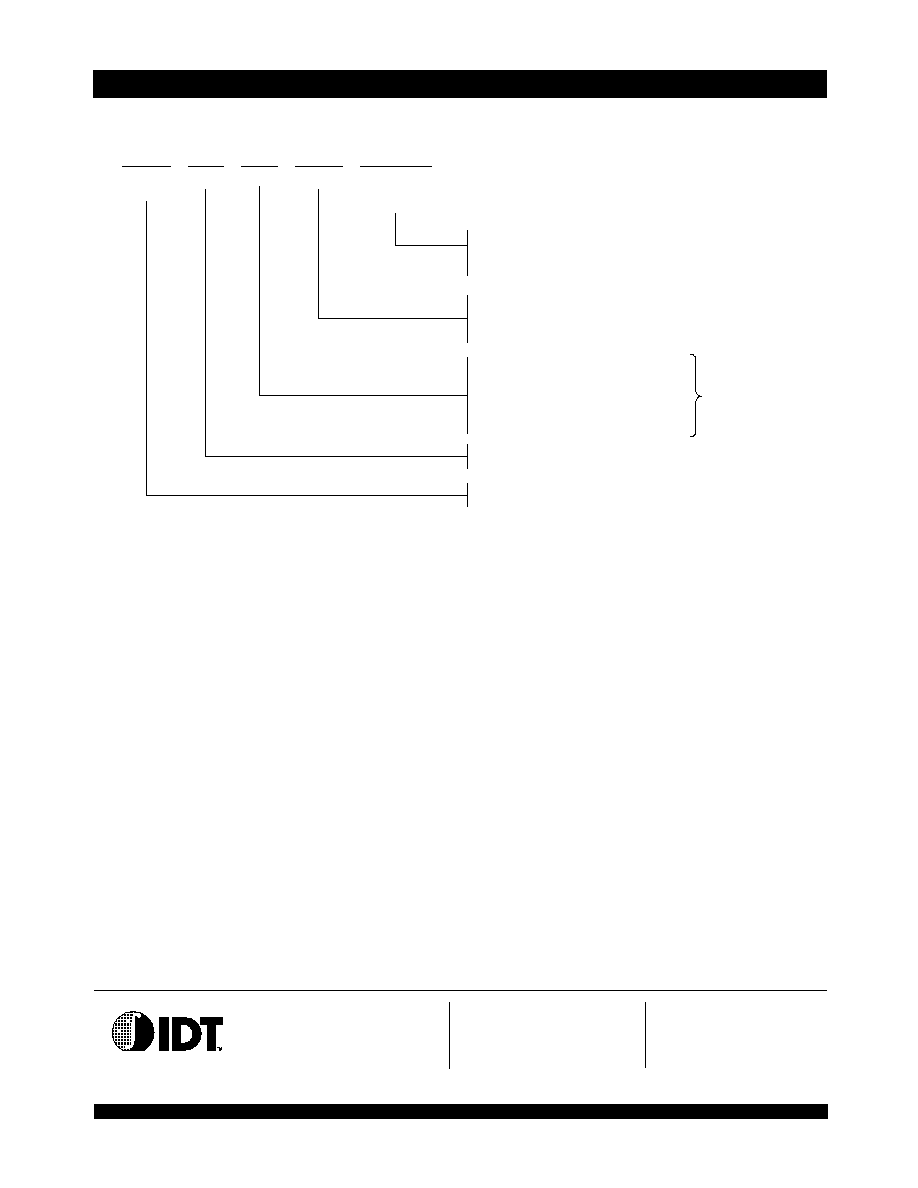
Functional Block Diagram
NOTE:
1.
IDT7133 (MASTER):
BUSY is open drain output and requires pull-up resistor.
IDT7143 (SLAVE):
BUSY is input.
x
x
x
x
x
BUSY output flag on IDT7133; BUSY input on IDT7143
x
x
x
x
x
Fully asynchronous operation from either port
x
x
x
x
x
Battery backup operation≠2V data retention
x
x
x
x
x
TTL-compatible; single 5V (±10%) power supply
x
x
x
x
x
Available in 68-pin ceramic PGA, Flatpack, PLCC and 100-
pin TQFP
x
x
x
x
x
Military product compliant to MIL-PRF-38535 QML
x
x
x
x
x
Industrial temperature range (≠40∞C to +85∞C) is available
for selected speeds
Description
The IDT7133/7143 are high-speed 2K x 16 Dual-Port Static RAMs.
The IDT7133 is designed to be used as a stand-alone 16-bit Dual-Port
RAM or as a "MASTER" Dual-Port RAM together with the IDT7143
"SLAVE" Dual-Port in 32-bit-or-more word width systems. Using the
IDT MASTER/SLAVE Dual-Port RAM approach in 32-bit-or-wider
I/O
CONTROL
MEMORY
ARRAY
ARBITRATION
LOGIC
(IDT7133 ONLY)
R/
W
LUB
CE
L
R/
W
LLB
OE
L
I/O
0L
- I/O
7L
BUSY
L
A
0L
CE
L
R/
W
RUB
CE
R
R/
W
RLB
OE
R
I/O
8R
- I/O
15R
I/O
0R
- I/O
7R
BUSY
R
(1)
A
0R
CE
R
2746 drw 01
A
10L
ADDRESS
DECODER
A
10R
I/O
CONTROL
ADDRESS
DECODER
11
11
(1)
I/O
8L
- I/O
15L
6.42
IDT7133SA/LA, IDT7143SA/LA
High-Speed 2K x 16 Dual-Port RAM Military, Industrial and Commercial Temperature Ranges
2
2746 drw 02
10
11
12
13
14
15
16
IDT7133/43
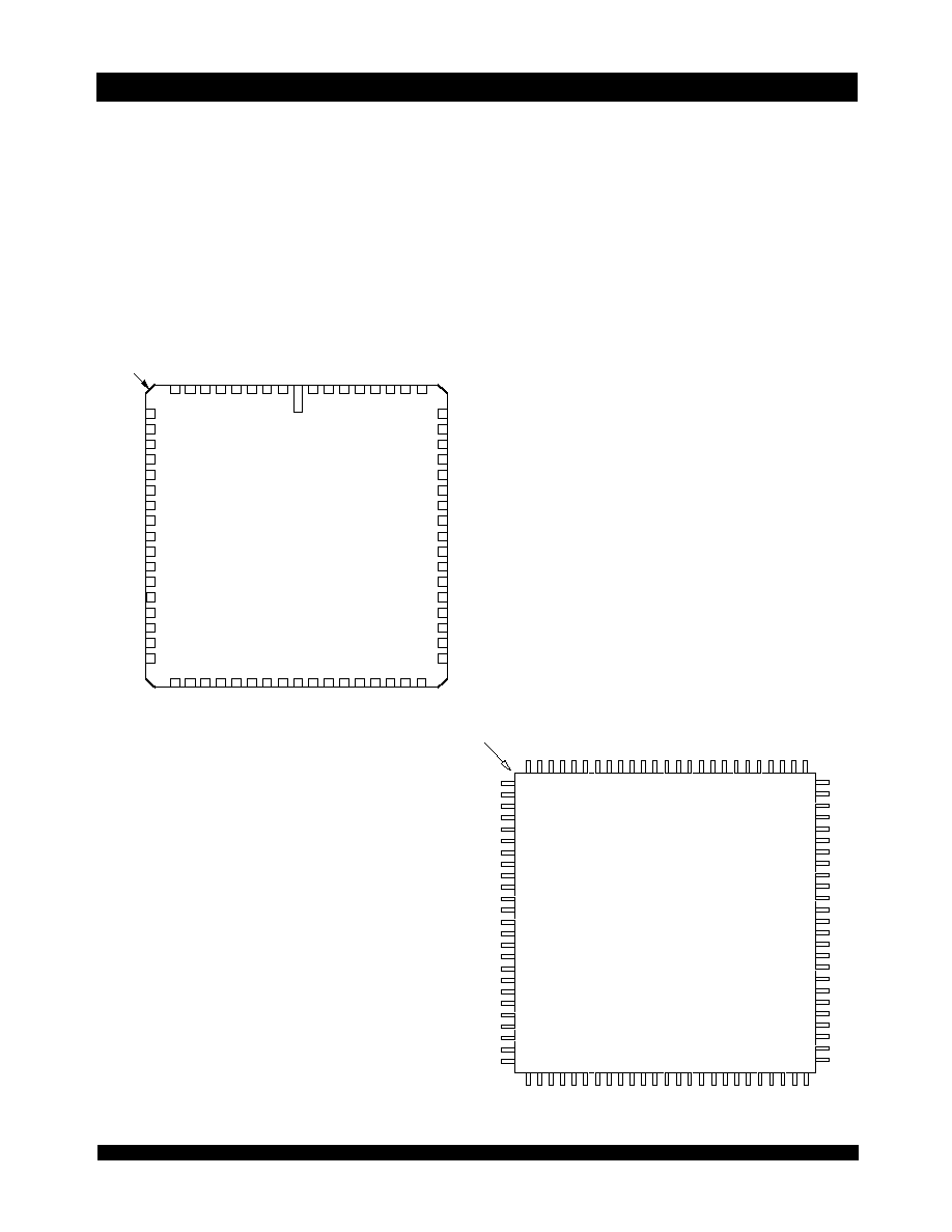
J68-1 / F68-1
(4)
68-Pin PLCC/Flatpack
Top View
(5)
50
49
48
47
46
45
44
INDEX
17
18
19
20
21
22
23
24
25
26
51
52
53
54
55
56
57
58
59
60
9
8
7
6
5
4
3
2
1
68 67 66 65 64 63 62 61
27 28 29 30 31 32 33 34 35 36 37 38 39 40 41 42 43
A
6L
A
5L
A
4L
A
3L
A
2L
A
1L
A
0L
A
0R
A
1R
A
2R
A
3R
A
4R
A
5R
BUSY
L
BUSY
R
CE
L
CE
R
I/O
9L
I/O
10L
I/O
11L
I/O
13L
I/O
14L
I/O
15L
V
CC
(1)
I/O
0R
I/O
1R
I/O
2R
I/O
3R
I/O
4R
I/O
5R
I/O
6R
I/O
7R
I
/
O
1
L
I
/
O
2
L
I
/
O
3
L
I
/
O
4
L
I
/
O
5
L
I
/
O
6
L
I
/
O
7
L
I
/
O
8
L
V
C
C
(
1
)
A
1
0
L
A
9
L
A
8
L
A
7
L
R
/
W
L
L
B
O
E
L
I
/
O
9
R
I
/
O
1
0
R
I
/
O
1
2
R
I
/
O
1
3
R
I
/
O
1
4
R
I
/
O
1
5
R
A
6
R
A
7
R
A
8
R
A
9
R
I
/
O
8
R
A
1
0
R
G
N
D
(
2
)
O
E
R
R
/
W
R
L
B
R
/
W
R
U
B
I
/
O
1
1
R
I
/
O
0
L
I/O
12L
GND
(2)
R
/
W
L
U
B
Pin Configurations
(1,2,3)
memory system applications results in full-speed, error-free operation
without the need for additional discrete logic.
Both devices provide two independent ports with separate control,
address, and I/O pins that permit independent, asynchronous access
for reads or writes to any location in memory. An automatic power
down feature, controlled by
CE, permits the on-chip circuitry of each
port to enter a very low standby power mode.
Fabricated using IDT's CMOS high-performance technology, these
devices typically operate on only 1,150mW of power. Low-power (LA)
versions offer battery backup data retention capability, with each port
typically consuming 200µW for a 2V battery.
The IDT7133/7143 devices have identical pinouts. Each is packed
in a 68-pin ceramic PGA, 68-pin flatpack, 68-pin PLCC and 100-pin
TQFP. Military grade product is manufactured in compliance with the
latest revision of MIL-PRF-38535 QML, making it ideally suited to
military temperature applications demanding the highest level of
performance and reliability.
NOTES:
1.
Both V
CC
pins must be connected to the power supply to ensure reliable
operation.
2.
Both GND pins must be connected to the ground supply to ensure reliable
operation.
3.
J68-Package body is approximately 0.95 in x 0.95 in x 0.17 in.
F68-Package body is approximately 1.18 in x 1.18 in x 0.16 in.
PN100-Package body is approximately 14mm x 14mm x 1.4mm.
4.
This package code is used to reference the package diagram.
5.
This text does not indicate orientation of the actual part-marking.
Index
1
2
3
4
5
6
7
8
9
10
11
12
13
14
15
16
17
18
19
20
21
22
23
24
25
75
74
73
72
71
70
69
68
67
66
65
64
63
62
61
60
59
58
57
56
55
54
53
52
51
26 27 28 29 30 31 32 33 34 35 36 37 38 39 40 41 42 43 44 45 46 47 48 49 50
100 99 98 97 96 95 94 93 92 91 90 89 88 87 86 85 84 83 82 81 80 79 78 77 76
IDT7133/43PF
PN100-1
(4)
100-Pin TQFP
Top View
(5)
N/C
N/C
N/C
N/C
I/O
10L
I/O
11L
I/O
12L
I/O
13L
GND
I/O
14L
I/O
15L
V
CC
GND
I/O
0R
I/O
1R
I/O
2R
I/O
3R
V
CC
I/O
4R
I/O
5R
I/O
6R
N/C
N/C
N/C
N/C
2746 drw 03
N/C
N/C
N/C
N/C
A
5L
A
4L
A
3L
A
2L
A
1L
A
0L
N/C
GND
N/C
BUSY
R
N/C
A
0R
N/C
N/C
N/C
N/C
BUSY
L
A
1R
A
2R
A
3R
A
4R
I
/
O
9
L
I
/
O
8
L
I
/
O
7
L
I
/
O
6
L
I
/
O
5
L
I
/
O
4
L
I
/
O
3
L
I
/
O
2
L
G
N
D
I
/
O
1
L
I
/
O
0
L
O
E
L
V
C
C
R
/
W
L
L
B
C
E
L
R
/
W
L
U
B
N
/
C
N
/
C
N
/
C
A
1
0
L
A
9
L
A
8
L
A
7
L
A
6
L
I
/
O
7
R
I
/
O
8
R
I
/
O
9
R
I
/
O
1
0
R
I
/
O
1
1
R
I
/
O
1
2
R
I
/
O
1
3
R
I
/
O
1
4
R
G
N
D
I
/
O
1
5
R
R
/
W
R
L
B
G
N
D
N
/
C
N
/
C
A
1
0
R
A
9
R
A
8
R
A
7
R
A
6
R
A
5
R
N
/
C
N
/
C
N
/
C
O
E
R
C
E
R
R
/
W
R
U
B
,

6.42
IDT7133SA/LA, IDT7143SA/LA
High-Speed 2K x 16 Dual-Port RAM Military, Industrial and Commercial Temperature Ranges
3
Pin Configurations
(1,2,3)
(con't.)
NOTES:
1.
Both V
CC
pins must be connected to the power supply to ensure reliable operation.
2.
Both GND pins must be connected to the ground supply to ensure reliable operation.
3.
Package body is approximately 1.18 in x 1.18 in x 0.16 in.
4.
This package code is used to reference the package diagram.
5.
This text does not indicate orientation of the actual part-marking.
Pin Names
2746 drw 04
I/O
0L
V
CC(1)
A
10L
A
9L
A
8L
A
7L
A
6L
A
5L
A
4L
A
3L
51
I/O
1L
I/O
2L
I/O
3L
I/O
4L
I/O
5L
I/O
6L
I/O
7L
I/O
8L
I/O
9L
I/O
10L
I/O
11L
I/O
12L
I/O
13L
I/O
14L
I/O
15L
V
CC(1)
GND
(2
)
I/O
0R
I/O
1R
I/O
2R
I/O
3R
I/O
4R
I/O
5R
I/O
6R
I/O
7R
I/O
8R
I/O
9R
I/O
10R
I/O
11R
I/O
12R
I/O
13R
I/O
14R
I/O
15R
A
2L
A
1L
A
0L
R/
W
LUB
R/
W
LLB
OE
L
A
2R
A
3R
A
4R
A
5R
A
6R
A
7R
A
8R
A
9R
A
10R
R/
W
RLB
R/
W
RUB
OE
R
GND
(2)
BUSY
L
BUSY
R
CE
L
CE
R
50
48
46
44
42
40
38
36
A
0R
A
1R
52
49
47
45
43
41
39
37
35
53
34
54
55
56
57
58
59
60
61
62
63
64
65
66
67
1
68
2
3
4
5
6
7
8
9
10
11
12
13
14
15
16
18
17
19
20
21
22
23
24
25
26
27
28
29
30
31
32
33
IDT7133/43G
GU68-1
(4)
68-Pin PGA
Top View
(5)
Pin 1
Designator
A
B
C
D
E
F
G
H
J
K
L
01
02
03
04
05
06
07
08
09
10
11
Left Port
Right Port
Names
CE
L
CE
R
Chip Enable
R/W
LUB
R/W
RUB
Upper Byte Read/Write Enable
R/W
LLB
R/W
RLB
Lower Byte Read/Write Enable
OE
L
OE
R
Output Enable
A
0L
- A
10L
A
0R
- A
10R
Address
I/O
0L
- I/O
15L
I/O
0R
- I/O
15R
Data Input/Output
BUSY
L
BUSY
R
Busy Flag
V
CC
Power
GND
Ground
2746 tbl 01

6.42
IDT7133SA/LA, IDT7143SA/LA
High-Speed 2K x 16 Dual-Port RAM Military, Industrial and Commercial Temperature Ranges
4
Capacitance
(T
A
= +25∞C, f = 1.0mhz)
Recommended DC Operating
Conditions
Maximum Operating
Temperature and Supply Voltage
(1,2)
Absolute Maximum Ratings
(1)
DC Electrical Characteristics Over the Operating
Temperature and Supply Voltage Range
(Either port, V
CC
= 5.0V ± 10%)
NOTE:
1.
At Vcc < 2.0V, input leakages are undefined.
NOTES:
1.
Stresses greater than those listed under ABSOLUTE MAXIMUM RATINGS may
cause permanent damage to the device. This is a stress rating only and functional
operation of the device at these or any other conditions above those indicated in
the operational sections of this specification is not implied. Exposure to absolute
maximum rating conditions for extended periods may affect reliability.
2.
V
TERM
must not exceed Vcc + 10% for more than 25% of the cycle time or 10ns
maximum, and is limited to < 20mA for the period of V
TERM
> Vcc + 10%.
NOTES:
1.
This parameter is determined by device characterization but is not production
tested.
2.
3dV references the interpolated capacitance when the input and output switch from
0V to 3V or from 3V to 0V.
NOTES:
1. This is the parameter T
A
. This is the "instant on" case temperature.
NOTES:
1.
V
IL
(min.) = -1.5V for pulse width less than 10ns.
2.
V
TERM
must not exceed Vcc + 10%.
Symbol
Rating
Commercial
& Industrial
Military
Unit
V
TERM
(2)
Terminal Voltage
with Respect
to GND
-0.5 to +7.0
-0.5 to +7.0
V
T
BIAS
Temperature
Under Bias
-55 to +125
-65 to +135
o
C
T
STG
Storage
Temperature
-65 to +150
-65 to +150
o
C
P
T
(3)
Power
Dissipation
2.0
2.0
W
I
OUT
DC Output
Current
50
50
mA
2746 tbl 02
Grade
Ambient
Temperature
GND
Vcc
Military
-55
O
C to +125
O
C
0V
5.0V
+
10%
Commercial
0
O
C to +70
O
C
0V
5.0V
+
10%
Industrial
-40
O
C to +85
O
C
0V
5.0V
+
10%
2746 tbl 04
Symbol
Parameter
(1)
Conditions
(2)
Max.
Unit
C
IN
Input Capacitance
V
IN
= 3dV
11
pF
C
OUT
Output Capacitance
V
OUT
= 3dV
11
pF
2746 tbl 03
Symbol
Parameter
Min.
Typ.
Max.
Unit
V
CC
Supply Voltage
4.5
5.0
5.5
V
GND
Ground
0
0
0
V
V
IH
Input High Voltage
2.2
____
6.0
(2)
V
V
IL
Input Low Voltage
-0.5
(1)
____
0.8
V
2746 tbl 05
Symbol
Parameter
Test Conditions
7133SA
7143SA
7133LA
7143LA
Unit
Min.
Max.
Min.
Max.
|I
LI
|
Input Leakage Current
(1)
V
CC
= 5.5V, V
IN
= 0V to V
CC
___
10
___
5
µA
|I
LO
|
Output Leakage Current
CE = V
IH
, V
OUT
= 0V to V
CC
___
10
___
5
µA
V
OL
Output Low Voltage (I/O
0
-I/O
15
)
I
OL
= 4mA
___
0.4
___
0.4
V
V
OL
Open Drain Output Low Voltage
(
BUSY)
I
OL
= 16mA
___
0.5
___
0.5
V
V
OH
Output High Voltage
I
OH
= -4mA
2.4
___
2.4
___
V
2746 tbl 06
6.42
IDT7133SA/LA, IDT7143SA/LA
High-Speed 2K x 16 Dual-Port RAM Military, Industrial and Commercial Temperature Ranges
5
NOTES:
1.
V
CC
= 5V, T
A
= +25∞C for Typ., and are not production tested. I
CCDC
= 180mA (typ.)
2.
'X' in part number indicates power rating (SA or LA)
3.
At f = f
MAX
,
address and control lines (except Output Enable) are cycling at the maximum frequency read cycle of 1/ t
RC,
and using "AC Test Conditions" of input levels of
GND to 3V.
4.
f = 0 means no address or control lines change. Applies only to inputs at CMOS level standby.
5.
Port "A" may be either left or right port. Port "B" is the opposite from port "A".
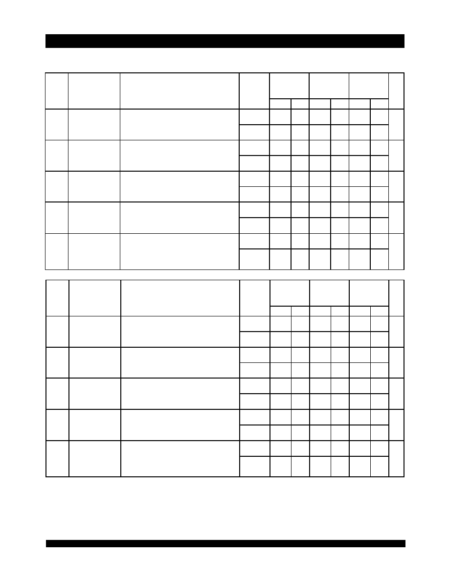
DC Electrical Characteristics Operating
Temperature and Supply Voltage Range
(2)
(V
CC
= 5.0V ± 10%)
7133X20
7143X20
Com'l Only
7133X25
7143X25
Com'l, Ind
& Military
7133X35
7143X35
Com'l, Ind
& Military
Symbol
Parameter
Test Condition
Version
Typ.
(1)
Max.
Typ.
(1)
Max.
Typ.
(1)
Max.
Unit
I
CC
Dynamic Operating
Current
(Both Ports Active)
CE = V
IL
, Outputs Disabled
f = f
MAX
(3)
COM'L
S
L
250
230
310
280
250
230
300
270
240
210
295
250
mA
MIL &
IND
S
L
____
____
____
____
250
230
330
300
240
220
325
295
I
SB1
Standby Current
(Both Ports - TTL
Level Inputs)
CE
L
and
CE
R
= V
IH
f = f
MAX
(3)
COM'L
S
L
25
25
80
70
25
25
80
70
25
25
70
60
mA
MIL &
IND
S
L
____
____
____
____
25
25
90
80
25
25
75
65
I
SB2
Standby Current
(One Port - TTL
Level Inputs)
CE
"A"
= V
IL
and
CE
"B"
= V
IH
(4)
f=f
MAX
(3)
Active Port Outputs Disabled
COM'L
S
L
140
120
200
180
140
100
200
170
120
100
180
160
mA
MIL &
IND
S
L
____
____
____
____
140
100
230
190
120
100
200
180
I
SB3
Full Standby Current
(Both Ports -
CMOS Level Inputs)
Both Ports
CE
L
and
CE
R
> V
CC
- 0.2V
V
IN
> V
CC
- 0.2V or
V
IN
< 0.2V, f = 0
(4)
COM'L
S
L
1.0
0.2
15
5
1.0
0.2
15
4
1.0
0.2
15
4
mA
MIL &
IND
S
L
____
____
____
____
1.0
0.2
30
10
1.0
0.2
30
10
I
SB4
Full Standby Current
(One Port -
CMOS Level Inputs)
CE
"A"
< 0.2V and
CE
"B"
> V
CC
- 0.2V
(5)
V
IN
> V
CC
- 0.2V or V
IN
< 0.2V
Active Port Outputs Disabled
f = f
MAX
(3)
COM'L
S
L
140
120
190
170
140
120
190
170
120
100
170
150
mA
MIL &
IND
S
L
____
____
____
____
140
120
220
200
120
100
190
170
2746 tbl 07a
7133X45
7143X45
Com'l &
Military
7133X55
7143X55
Com'l, Ind
& Military
7133X70/90
7143X70/90
Com'l &
Military
Symbol
Parameter
Test Condition
Version
Typ.
(1)
Max.
Typ.
(1)
Max.
Typ.
(1)
Max.
Unit
I
CC
Dynamic Operating
Current
(Both Ports Active)
CE = V
IL
, Outputs Disabled
f = f
MAX
(3)
COM'L
S
L
230
210
290
250
230
210
285
250
230
210
280
250
mA
MIL &
IND
S
L
230
210
320
290
230
210
315
285
230
210
310
280
I
SB1
Standby Current
(Both Ports - TTL
Level Inputs)
CE
L
and
CE
R
= V
IH
f = f
MAX
(3)
COM'L
S
L
25
25
75
65
25
25
70
60
25
25
70
60
mA
MIL &
IND
S
L
25
25
80
70
25
25
80
70
25
25
75
65
I
SB2
Standby Current
(One Port - TTL
Level Inputs)
CE
"A"
= V
IL
and
CE
"B"
= V
IH
(4)
f=f
MAX
(3)
Active Port Outputs Disabled
COM'L
S
L
120
100
190
170
120
100
180
160
120
100
180
160
mA
MIL &
IND
S
L
120
100
210
190
120
100
210
190
120
100
200
180
I
SB3
Full Standby Current
(Both Ports -
CMOS Level Inputs)
Both Ports
CE
L
and
CE
R
> V
CC
- 0.2V
V
IN
> V
CC
- 0.2V or
V
IN
< 0.2V, f = 0
(4)
COM'L
S
L
1.0
0.2
15
4
1.0
0.2
15
4
1.0
0.2
15
4
mA
MIL &
IND
S
L
1.0
0.2
30
10
1.0
0.2
30
10
1.0
0.2
30
10
I
SB4
Full Standby Current
(One Port -
CMOS Level Inputs)
CE
"A"
< 0.2V and
CE
"B"
> V
CC
- 0.2V
(5)
V
IN
> V
CC
- 0.2V or V
IN
< 0.2V
Active Port Outputs Disabled
f = f
MAX
(3)
COM'L
S
L
120
100
180
160
120
100
170
150
120
100
170
150
mA
MIL &
IND
S
L
120
100
200
180
120
100
200
180
120
100
190
170
2746 tbl 07b

6.42
IDT7133SA/LA, IDT7143SA/LA
High-Speed 2K x 16 Dual-Port RAM Military, Industrial and Commercial Temperature Ranges
6
2746 drw 06
DATA
OUT
775
1250
30pF
5V
DATA
OUT
775
1250
5pF*
5V
BUSY
270
30pF
5V
Data Retention Waveform
AC Test Conditions
Data Retention Characteristics
(LA Version Only) V
LC
= 0.2V, V
HC
= V
CC
- 0.2V
NOTES:
1.
Vcc = 2V, T
A
= +25∞C, and are not production tested.
2.
t
RC
= Read Cycle Time
3.
This parameter is guaranteed by device characterization but is not production tested.
Figure 2. Output Load
(for t
LZ
, t
HZ
, t
WZ
, t
OW
)
*Including scope and jig
Figure 1. AC Output Test Load
Figure 3.
BUSY Output Load
(IDT7133 only)
7133LA/7143LA
Symbol
Parameter
Test Condition
Min.
Typ.
(1)
Max.
Unit
V
DR
V
CC
for Data Retention
V
CC
= 2V
2.0
___
___
V
I
CCDR
Data Retention Current
CE > V
HC
V
IN
> V
HC
or < V
LC
MIL. & IND.
___
100
4000
µA
COM'L.
___
100
1500
t
CDR
(3)
Chip Deselect to Data Retention Time
0
___
___
V
t
R
(3)
Operation Recovery Time
t
RC
(2)
___
___
V
2746 tbl 08
Input Pulse Levels
Input Rise/Fall Times
Input Timing Reference Levels
Output Reference Levels
Output Load
GND to 3.0V
5ns Max.
1.5V
1.5V
Figures 1, 2 and 3
2746 tbl 09
2746 drw 05
t
CDR
t
R
CE
V
CC
DATA RETENTION MODE
V
DR
V
DR
> 2V
4.5V
4.5V
V
IH
V
IH

6.42
IDT7133SA/LA, IDT7143SA/LA
High-Speed 2K x 16 Dual-Port RAM Military, Industrial and Commercial Temperature Ranges
7
AC Electrical Characteristics Over the
Operating Temperature and Supply Voltage
(3)
NOTES:
1. Transition is measured 0mV fromLow or High-impedance voltage with load (Figure 2).
2.
This parameter is guaranteed by device characterization, but is not production tested.
3.
'X' in part number indicates power rating (SA or LA).
7133X20
7143X20
Com'l Only
7133X25
7143X25
Com'l, Ind
& Military
7133X35
7143X35
Com'l, Ind
& Military
Unit
Symbol
Parameter
Min.
Max.
Min.
Max.
Min.
Max.
READ CYCLE
t
RC
Read Cycle Time
20
____
25
____
35
____
ns
t
AA
Address Access Time
____
20
____
25
____
35
ns
t
ACE
Chip Enable Access Time
____
20
____
25
____
35
ns
t
AOE
Output Enable Access Time
____
12
____
15
____
20
ns
t
OH
Output Hold from Address Change
0
____
0
____
0
____
ns
t
LZ
Output Low-Z Time
(1,2)
0
____
0
____
0
____
ns
t
HZ
Output High-Z Time
(1,2)
____
12
____
15
____
20
ns
t
PU
Chip Enable to Power Up Time
(2)
0
____
0
____
0
____
ns
t
PD
Chip Disable to Power Down Time
(2)
____
20
____
50
____
50
ns
2746 tbl 10a
7133X45
7143X45
Com'l &
Military
7133X55
7143X55
Com'l, Ind
& Military
7133X70/90
7143X70/90
Com'l &
Military
Unit
Symbol
Parameter
Min.
Max.
Min.
Max.
Min.
Max.
READ CYCLE
t
RC
Read Cycle Time
45
____
55
____
70/90
____
ns
t
AA
Address Access Time
____
45
____
55
____
70/90
ns
t
ACE
Chip Enable Access Time
____
45
____
55
____
70/90
ns
t
AOE
Output Enable Access Time
____
25
____
30
____
40/40
ns
t
OH
Output Hold from Address Change
0
____
0
____
0/0
____
ns
t
LZ
Output Low-Z Time
(1,2)
0
____
5
____
5/5
____
ns
t
HZ
Output High-Z Time
(1,2)
____
20
____
20
____
25/25
ns
t
PU
Chip Enable to Power Up Time
(2)
0
____
0
____
0/0
____
ns
t
PD
Chip Disable to Power Down Time
(2)
____
50
____
50
____
50/50
ns
2746 tbl 10b
6.42
IDT7133SA/LA, IDT7143SA/LA
High-Speed 2K x 16 Dual-Port RAM Military, Industrial and Commercial Temperature Ranges
8
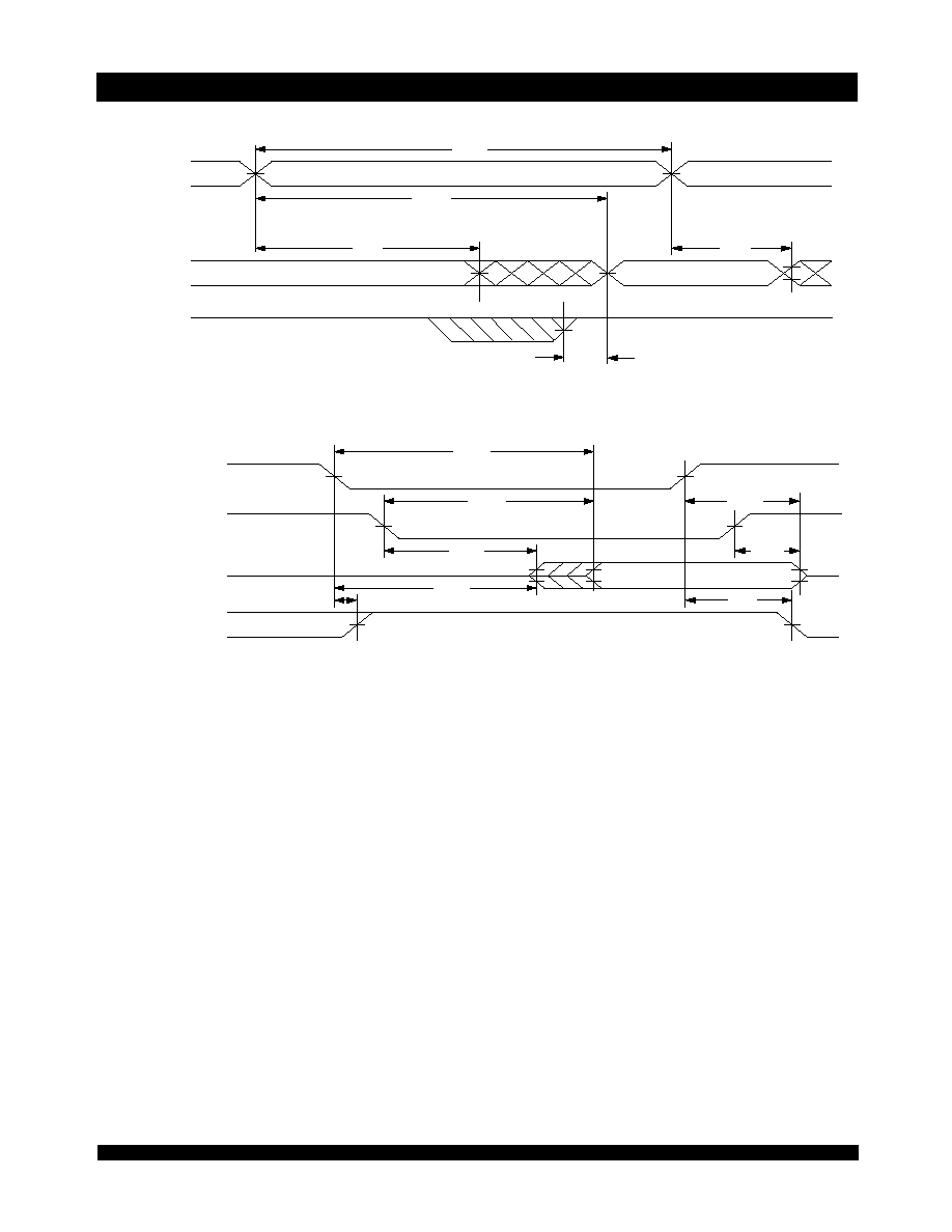
TIMING WAVEFORM OF READ CYCLE NO. 1, EITHER SIDE
(5)
TIMING WAVEFORM OF READ CYCLE NO. 2, EITHER SIDE
(5)
NOTES:
1.
Timing depends on which signal is asserted last,
OE or CE.
2.
Timing depends on which signal is deasserted first,
OE or CE.
3.
t
BDD
delay is required only in a case where the opposite port is completing a write operation to the same address location. For simultaneous read operations,
BUSY has no
relationship to valid output data.
4.
Start of valid data depends on which timing becomes effective last, t
AOE
, t
ACE
, t
AA,
or t
BDD
.
5.
R/W = V
IH
, and the address is valid prior to or coincidental with
CE transition LOW.
2746 drw 07
t
AA
t
OH
t
OH
DATA
OUT
ADDRESS
t
RC
DATA VALID
PREVIOUS DATA VALID
BUSY
OUT
t
BDD
(3,4)
2746 drw 08
t
AOE
t
LZ
t
HZ
DATA
OUT
CE
t
ACE
VALID DATA
OE
CURRENT
I
CC
I
SB
t
PU
50%
t
LZ
t
PD
50%
t
HZ
(1)
(4)
(1)
(4)
(2)
(2)
6.42
IDT7133SA/LA, IDT7143SA/LA
High-Speed 2K x 16 Dual-Port RAM Military, Industrial and Commercial Temperature Ranges
9
AC Electrical Characteristics Over the
Operating Temperature and Supply Voltage
(5)
NOTES:
1. Transition is measured 0mV from Low or High-impedance voltage from the Output Test Load (Figure 2).
2.
This parameter is guaranteed by device characterization but not production tested.
3.
For MASTER/SLAVE combination, t
WC
= t
BAA
+ t
WR
+ t
WP
, since R/
W = V
IL
must occur after t
BAA.
4.
The specification for t
DH
must be met by the device supplying write data to the RAM under all operation conditions. Although t
DH
and t
OW
values will very over voltage and
temperature, the actual t
DH
will always be smaller than the actual t
OW
.
5.
'X' in part number indicates power rating (SA or LA).
Symbol
Parameter
7133X20
7143X20
Com'l Only
7133X25
7143X25
Com'l, Ind
& Military
7133X35
7143X35
Com'l, Ind
& Military
Unit
Min.
Max.
Min.
Max.
Min.
Max.
WRITE CYCLE
t
WC
Write Cycle Time
(3)
20
____
25
____
35
____
ns
t
EW
Chip Enable to End-of-Write
15
____
20
____
25
____
ns
t
AW
Address Valid to End-of-Write
15
____
20
____
25
____
ns
t
AS
Address Set-up Time
0
____
0
____
0
____
ns
t
WP
Write Pulse Width
15
____
20
____
25
____
ns
t
WR
Write Recovery Time
0
____
0
____
0
____
ns
t
DW
Data Valid to End-of-Write
15
____
15
____
20
____
ns
t
HZ
Output High-Z Time
(1,2)
____
12
____
15
____
20
ns
t
DH
Data Hold Time
(4)
0
____
0
____
0
____
ns
t
WZ
Write Enable to Output in High-Z
(1,2)
____
12
____
15
____
20
ns
t
OW
Output Active from End-of-Write
(1,2,4)
0
____
0
____
0
____
ns
2746 tbl 11a
Symbol
Parameter
7133X45
7143X45
Com'l &
Military
7133X55
7143X55
Com'l, Ind
& Military
7133X70/90
7143X70/90
Com'l &
Military
Unit
Min.
Max.
Min.
Max.
Min.
Max.
WRITE CYCLE
t
WC
Write Cycle Time
(3)
45
____
55
____
70/90
____
ns
t
EW
Chip Enable to End-of-Write
30
____
40
____
50/50
____
ns
t
AW
Address Valid to End-of-Write
30
____
40
____
50/50
____
ns
t
AS
Address Set-up Time
0
____
0
____
0/0
____
ns
t
WP
Write Pulse Width
30
____
40
____
50/50
____
ns
t
WR
Write Recovery Time
0
____
0
____
0/0
____
ns
t
DW
Data Valid to End-of-Write
20
____
25
____
30/30
____
ns
t
HZ
Output High-Z Time
(1,2)
____
20
____
20
____
25/25
ns
t
DH
Data Hold Time
(4)
5
____
5
____
5/5
____
ns
t
WZ
Write Enable to Output in High-Z
(1,2)
____
20
____
20
____
25/25
ns
t
OW
Output Active from End-of-Write
(1,2,4)
5
____
5
____
5/5
____
ns
2746 tbl 11b

6.42
IDT7133SA/LA, IDT7143SA/LA
High-Speed 2K x 16 Dual-Port RAM Military, Industrial and Commercial Temperature Ranges
10
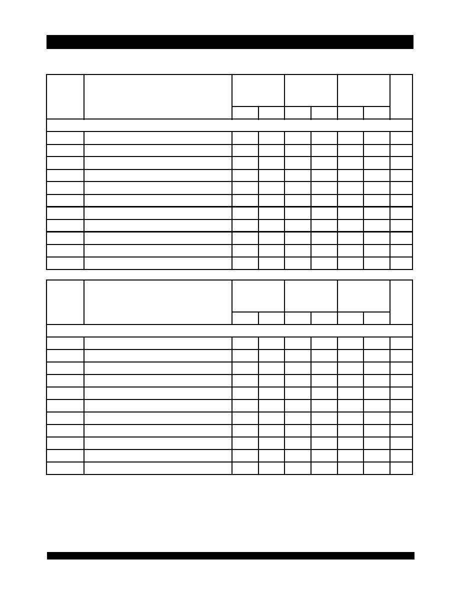
AC Electrical Characteristics Over the
Operating Temperature and Supply Voltage
(6)
NOTES:
1.
Port-to-port delay through RAM cells from writing port to reading port, refer to "Timing Waveform of Write with Port-to-Port Read and Busy".
2.
t
BDD
is calculated parameter and is greater of 0, t
WDD
- t
WP
(actual) or t
DDD
- t
DW
(actual).
3.
To ensure that the earlier of the two ports wins.
4.
To ensure that the write cycle is inhibited on port "B" during contention on port "A".
5.
To ensure that a write cycle is completed on port "B" after contention on port "A".
6.
'X' in part number indicates power rating (SA or LA).
7133X20
7143X20
Com'l Only
7133X25
7143X25
Com'l, Ind
& Military
7133X35
7143X35
Com'l, Ind
& Military
Symbol
Parameter
Min.
Max.
Min.
Max.
Min.
Max.
Unit
BUSY TIMING (For MASTER 71V33)
t
BAA
BUSY Access Time from Address
____
20
____
20
____
30
ns
t
BDA
BUSY Disable Time from Address
____
20
____
20
____
30
ns
t
BAC
BUSY Access Time from Chip Enable
____
20
____
20
____
25
ns
t
BDC
BUSY Disable Time from Chip Enable
____
17
____
20
____
25
ns
t
WDD
Write Pulse to Data Delay
(1)
____
40
____
50
____
60
ns
t
DDD
Write Data Valid to Read Data Delay
(1)
____
30
____
35
____
45
ns
t
BDD
BUSY Disable to Valid Data
(2)
____
25
____
30
____
35
ns
t
APS
Arbitration Priority Set-up Time
(3)
5
____
5
____
5
____
ns
t
WH
Write Hold After
BUSY
(5)
20
____
20
____
25
____
ns
BUSY INPUT TIMING (For SLAVE 71V43)
t
WB
BUSY Input to Write
(4)
0
____
0
____
0
____
ns
t
WH
Write Hold After
BUSY
(5)
20
____
20
____
25
____
ns
t
WDD
Write Pulse to Data Delay
(1)
____
40
____
50
____
60
ns
t
DDD
Write Data Valid to Read Data Delay
(1)
____
30
____
35
____
45
ns
2746 tbl 12a
7133X45
7143X45
Com'l &
Military
7133X55
7143X55
Com'l, Ind
& Military
7133X70/90
7143X70/90
Com'l &
Military
Symbol
Parameter
Min.
Max.
Min.
Max.
Min.
Max.
Unit
BUSY TIMING (For MASTER 71V33)
t
BAA
BUSY Access Time from Address
____
40
____
40
____
45/45
ns
t
BDA
BUSY Disable Time from Address
____
40
____
40
____
45/45
ns
t
BAC
BUSY Access Time from Chip Enable
____
30
____
35
____
35/35
ns
t
BDC
BUSY Disable Time from Chip Enable
____
25
____
30
____
30/30
ns
t
WDD
Write Pulse to Data Delay
(1)
____
80
____
80
____
90/90
ns
t
DDD
Write Data Valid to Read Data Delay
(1)
____
55
____
55
____
70/70
ns
t
BDD
BUSY Disable to Valid Data
(2)
____
40
____
40
____
40/40
ns
t
APS
Arbitration Priority Set-up Time
(3)
5
____
5
____
5/5
____
ns
t
WH
Write Hold After
BUSY
(5)
30
____
30
____
30/30
____
ns
BUSY INPUT TIMING (For SLAVE 71V43)
t
WB
BUSY Input to Write
(4)
0
____
0
____
0/0
____
ns
t
WH
Write Hold After
BUSY
(5)
30
____
30
____
30/30
____
ns
t
WDD
Write Pulse to Data Delay
(1)
____
80
____
80
____
90/90
ns
t
DDD
Write Data Valid to Read Data Delay
(1)
____
55
____
55
____
70/70
ns
2746 tbl 12b

6.42
IDT7133SA/LA, IDT7143SA/LA
High-Speed 2K x 16 Dual-Port RAM Military, Industrial and Commercial Temperature Ranges
11
NOTES:
1.
R/
W or CE must be HIGH during all address transitions.
2. A write occurs during the overlap (t
EW
or t
WP
) of a
CE = V
IL
and a R/
W = V
IL
.
3.
t
WR
is measured from the earlier of
CE or R/W going HIGH to the end of the write cycle.
4.
During this period, the I/O pins are in the output state, and input signals must not be applied.
5.
If the
CE LOW transition occurs simultaneously with or after the R/W LOW transition, the outputs remain in the High-impedance state.
6.
Timing depends on which enable signal (
CE or R/W) is asserted last.
7.
Timing depends on which enable signal is de-asserted first,
CE or OE.
8. If
OE is LOW during a R/W controlled write cycle, the write pulse width must be the larger of t
WP
or (t
WZ
+ t
DW
) to allow the I/O drivers to turn off and data to be placed
on the bus for the required t
DW
. If
OE is HIGH during an R/W controlled write cycle, this requirement does not apply and the write pulse can be as short as the
specified t
WP
.
9. R/
W for either upper or lower byte.
Write Cycle No. 2 (CE Controlled Timing)
(1,5)
Timing Waveform of Write Cycle No. 1 (R/W Controlled Timing)
(1,5,8)
CE
2746 drw 09
t
AW
t
AS
t
WR
t
DW
DATA
IN
ADDRESS
t
WC
R/
W
t
WP
t
DH
DATA
OUT
t
WZ
(7)
(4)
(2)
t
OW
OE
(9)
t
LZ
(7)
t
HZ
(6)
(3)
(4)
(7)
t
HZ
CE
2746 drw 10
t
AW
t
AS
t
WR
t
DW
DATA
IN
ADDRESS
t
WC
R/
W
t
EW
t
DH
(9)
(6)
(2)

6.42
IDT7133SA/LA, IDT7143SA/LA
High-Speed 2K x 16 Dual-Port RAM Military, Industrial and Commercial Temperature Ranges
12
2746 drw 11
t
DW
t
APS
ADDR
"A"
t
WC
MATCH
t
WP
R/
W
"A"
DATA
IN"A"
ADDR
"B"
t
DH
VALID
(1)
MATCH
BUSY
"B"
t
BDA
VALID
t
BDD
t
DDD
(4)
t
WDD
DATA
OUT "B"
Timing Waveform of Write with Port-to-Port Read and BUSY
(1,2,3)
Timing Waveform of Write with BUSY
(3)
NOTES:
1. t
WH
must be met for both
BUSY input (IDT7143, slave) and output (IDT7133, master).
2.
BUSY is asserted on port "B" blocking R/W
"B"
, until
BUSY
"B"
goes HIGH.
3. All timing is the same for left and right ports. Port "
A
" may be either left or right port. Port "
B
" is the opposite from port "
A
".
NOTES:
1. To ensure that the earlier of the two ports wins, t
APS
is ignored for Slave (IDT7143).
2.
CE
L
=
CE
R
= V
IL
3.
OE = V
IL
for the reading port.
4. All timing is the same for left and right ports. Port "A" may be either the left or right port. Port "B" is the port opposite from port "A".
2746 drw 12
R/
W
"A"
BUSY
"B"
t
WP
t
WB
R/
W
"B"
t
WH
(1)
(2)
,

6.42
IDT7133SA/LA, IDT7143SA/LA
High-Speed 2K x 16 Dual-Port RAM Military, Industrial and Commercial Temperature Ranges
13
Timing Waveform of BUSY Arbitration Controlled by CE Timing
(1)
Timing Waveform of BUSY Arbitration Controlled by Addresses
(1)
NOTES:
1. All timing is the same for left and right ports. Port "
A
" may be either the left or right port. Port "
B
" is the port opposite from port "
A
".
2. If t
APS
is not satisfied, the
BUSY will be asserted on one side or the other, but there is no guarantee on which side BUSY will be asserted
(IDT7133 only).
t
APS
(2)
2746 drw 13
ADDR
"A" AND "B"
ADDRESSES MATCH
CE
"B"
BUSY
"B"
t
BAC
t
BDC
CE
"A"
t
RC
2746 drw 14
ADDR
"A"
ADDRESSES MATCH
ADDR
"B"
BUSY
"B"
ADDRESSES DO NOT MATCH
t
WC
OR
t
APS
t
BAA
t
BDA
(2)

6.42
IDT7133SA/LA, IDT7143SA/LA
High-Speed 2K x 16 Dual-Port RAM Military, Industrial and Commercial Temperature Ranges
14
Functional Description
The IDT7133/43 provides two ports with separate control, address
and I/O pins that permit independent access for reads or writes to any
location in memory. The IDT7133/43 has an automatic power down
feature controlled by
CE. The CE controls on-chip power down circuitry
that permits the respective port to go into a standby mode when not
selected (
CE HIGH). When a port is enabled, access to the entire
memory array is permitted. Non-contention READ/WRITE conditions
are illustrated in Truth Table 1.
Busy Logic
Busy Logic provides a hardware indication that both ports of the
RAM have accessed the same location at the same time. It also allows
one of the two accesses to proceed and signals the other side that the
RAM is "busy". The
BUSY pin can then be used to stall the access until
the operation on the other side is completed. If a write operation has
been attempted from the side that receives a
BUSY indication, the
write signal is gated internally to prevent the write from proceeding.
The use of
BUSY logic is not required or desirable for all applica-
tions. In some cases it may be useful to logically OR the
BUSY outputs
together and use any
BUSY indication as an interrupt source to flag the
event of an illegal or illogical operation. If the write inhibit function of
BUSY logic is not desirable, the
BUSY logic can be disabled by using
the IDT7143 (SLAVE). In the IDT7143, the
BUSY pin operates solely
as a write inhibit input pin. Normal operation can be programmed by
tying the
BUSY pins HIGH. If desired, unintended write operations can
be prevented to a port by tying the
BUSY pin for that port LOW. The
BUSY outputs on the IDT 7133 RAM are open drain and require pull-
up resistors.
Width Expansion with Busy Logic
Master/Slave Arrays
When expanding an IDT7133/43 RAM array in width while using
BUSY logic, one master part is used to decide which side of the RAM
array will receive a
BUSY indication, and to output that indication. Any
number of slaves to be addressed in the same address range as the
master, use the
BUSY signal as a write inhibit signal. Thus on the
IDT7133 RAM the
BUSY pin is an output and on the IDT7143 RAM, the
BUSY pin is an input (see Figure 3).
Expanding the data bus width to 32 bits or more in a Dual-Port RAM
system implies that several chips will be active at the same time. If each
chip includes a hardware arbitrator, and the addresses for each chip
arrive at the same time, it is possible that one will activate its
BUSY
L
while another activates its
BUSY
R
signal. Both sides are now
BUSY
and the CPUs will await indefinitely for their port to become free.
To avoid the "Busy Lock-Out" problem, IDT has developed a
MASTER/SLAVE approach where only one hardware arbitrator, in the
MASTER, is used. The SLAVE has
BUSY inputs which allow an
interface to the MASTER with no external components and with a
speed advantage over other systems.
When expanding Dual-Port RAMs in width, the writing of the SLAVE
RAMs must be delayed until after the
BUSY input has settled.
Otherwise, the SLAVE chip may begin a write cycle during a contention
situation. Conversely, the write pulse must extend a hold time past
BUSY to ensure that a write cycle takes place after the contention is
resolved. This timing is inherent in all Dual-Port memory systems where
more than one chip is active at the same time.
The write pulse to the SLAVE should be delayed by the maximum
arbitration time of the MASTER. If, then, a contention occurs, the write
to the SLAVE will be inhibited due to
BUSY from the MASTER.
Figure 4. Busy and chip enable routing for both width and depth expansion
with the IDT7133 (MASTER) and the IDT7143 (SLAVE).
V
CC
R/
W
BUSY
R/
W
BUSY
IDT7133
MASTER
V
CC
R/
W
BUSY
R/
W
BUSY
R/
W
BUSY
R/
W
BUSY
LEFT
RIGHT
2746 drw 15
IDT7143
SLAVE
270
270

6.42
IDT7133SA/LA, IDT7143SA/LA
High-Speed 2K x 16 Dual-Port RAM Military, Industrial and Commercial Temperature Ranges
15
Truth Table I Non-Contention Read/Write Control
(4)
Truth Table II Address BUSY
Arbitration
NOTES:
1.
Pins
BUSY
L
and
BUSY
R
are both outputs on the IDT7133 (MASTER). Both are
inputs on the IDT7143 (SLAVE). On Slaves the
BUSY input internally inhibits
writes.
2.
"L" if the inputs to the opposite port were stable prior to the address and enable
inputs of this port. "H" if the inputs to the opposite port became stable after the
address and enable inputs of this port. If t
APS
is not met, either
BUSY
L
or
BUSY
R
= V
IL
will result
BUSY
L
and
BUSY
R
outputs can not be LOW simultaneously.
3.
Writes to the left port are internally ignored when
BUSY
L
outputs are driving LOW
regardless of actual logic level on the pin. Writes to the right port are internally
ignored when
BUSY
R
outputs are driving LOW regardless of actual logic level on
the pin.
NOTES:
1.
A
0L
- A
10L
A
0R
- A
10R
2.
If
BUSY = LOW, data is not written.
3.
If
BUSY = LOW, data may not be valid, see t
WDD
and t
DDD
timing.
4.
"H" = HIGH, "L" = LOW, "X" = Don't Care, "Z" = High-Impedance, "LB" = Lower Byte, "UB" = Upper Byte
LEFT OR RIGHT PORT
(1)
Function
R/
W
LB
R/
W
UB
CE
OE
I/O
0-7
I/O
8-15
X
X
H
X
Z
Z
Port Disabled and in Power Down Mode, I
SB2
, I
SB4
X
X
H
X
Z
Z
CE
R
= CE
L
= V
IH
, Power Down Mode, I
SB1
or I
SB3
L
L
L
X
DATA
IN
DATA
IN
Data on Lower Byte and Upper Byte Written into Memory
(2)
L
H
L
L
DATA
IN
DATA
OUT
Data on Lower Byte Written into Memory
(2)
, Data in Memory Output on
Upper Byte
(3)
H
L
L
L
DATA
OUT
DATA
IN
Data in Memory Output on Lower Byte
(3)
, Data on Upper Byte Written into
Memory
(2)
L
H
L
H
DATA
IN
Z
Data on Lower Byte Written into Memory
(2)
H
L
L
H
Z
DATA
IN
Data on Upper Byte Written into Memory
(2)
H
H
L
L
DATA
OUT
DATA
OUT
Data in Memory Output on Lower Byte and Upper Byte
H
H
L
H
Z
Z
High Impedance Outputs
2746 tbl 13
Inputs
Outputs
Function
CE
L
CE
R
A
0L
-A
10L
A
0R
-A
10R
BUSY
L
(1)
BUSY
R
(1)
X
X
NO MATCH
H
H
Normal
H
X
MATCH
H
H
Normal
X
H
MATCH
H
H
Normal
L
L
MATCH
(2)
(2)
Write Inhibit
(3)
2746 tbl 14
6.42
IDT7133SA/LA, IDT7143SA/LA
High-Speed 2K x 16 Dual-Port RAM Military, Industrial and Commercial Temperature Ranges
16
Ordering Information
XX
Power
XX
Speed
X
Package
X
Process/
Temperature
Range
Blank
I
B
Commercial (0
∞
C to +70
∞
C)
Industrial (-40
∞
C to +85
∞
C)
Military (-55
∞
C to +125
∞
C)
Compliant to MIL-PRF-38535 QML
J
G
F
PF
68-pin PLCC (J68-1)
68-pin PGA (GU68-1)
68-pin Flatplack (F68-1)
100-pin TQFP (PN100-1)
20
25
35
45
55
70
90
XXXX
Device
Type
IDT
Speed in nanoseconds
2746 drw 16
LA
SA
Low Power
Standard Power
7133
7143
32K (2K x 16-Bit) MASTER Dual-Port RAM
32K (2K x 16-Bit) SLAVE Dual-Port RAM
Commercial Only
Commercial, Industrial & Military
Commercial, Industrial & Military
Commercial & Military
Commercial, Industrial & Military
Commercial & Military
Commercial & Military
CORPORATE HEADQUARTERS
for SALES:
for Tech Support:
2975 Stender Way
800-345-7015 or 408-727-6116
831-754-4613
Santa Clara, CA 95054
fax: 408-492-8674
DualPortHelp@idt.com
www.idt.com
The IDT logo is a registered trademark of Integrated Device Technology, Inc.
Datasheet Document History
12/18/98:
Initiated datasheet document history
Converted to new format
Cosmetic and typographical corrections
Added additional notes to pin configurations
Page 2 corrected PN100 pinout
2/17/99:
Corrected PF ordering code
3/9/99:
Cosmetic and typographical corrections
6/9/99:
Changed drawing format
10/1/99:
Added Industrial Temperature Ranges and removed corresponding notes
11/10/99:
Replaced IDT logo
4/1/00:
Changed ±500mV to 0mV in notes
Page 2 Fixed overbar in pinout
6/26/00:
Page 4
Increased storage temperature parameters
Clarified T
A
parameter
Page 5
DC Electrical parameters≠changed wording from "open" to "disabled"