Integrated Device Technology, Inc.
COMMERCIAL TEMPERATURE RANGES
DECEMBER 1996
©
1996 Integrated Device Technology, Inc.
DSC-2704/5
SyncBiFIFO is a trademark and the IDT logo is a registered trademark of Integrated Device Technology, Inc.
IDT72605
IDT72615
CMOS SyncBiFIFO
TM
256 x 18 x 2 and 512 x 18 x 2
FEATURES:
∑ Two independent FIFO memories for fully bidirectional
data transfers
∑ 256 x 18 x 2 organization (IDT 72605)
∑ 512 x 18 x 2 organization (IDT 72615)
∑ Synchronous interface for fast (20ns) read and write
cycle times
∑ Each data port has an independent clock and read/write
control
∑ Output enable is provided on each port as a three-state
control of the data bus
∑ Built-in bypass path for direct data transfer between two
ports
∑ Two fixed flags, Empty and Full, for both the A-to-B and
the B-to-A FIFO
∑ Programmable flag offset can be set to any depth in the
FIFO
∑ The synchronous BiFIFO is packaged in a 64-pin TQFP
(Thin Quad Flatpack), 68-pin PGA and 68-pin PLCC
∑ Industrial temperature range (-40oC to +85oC) is avail-
able, tested to military electrical specifications
DESCRIPTION:
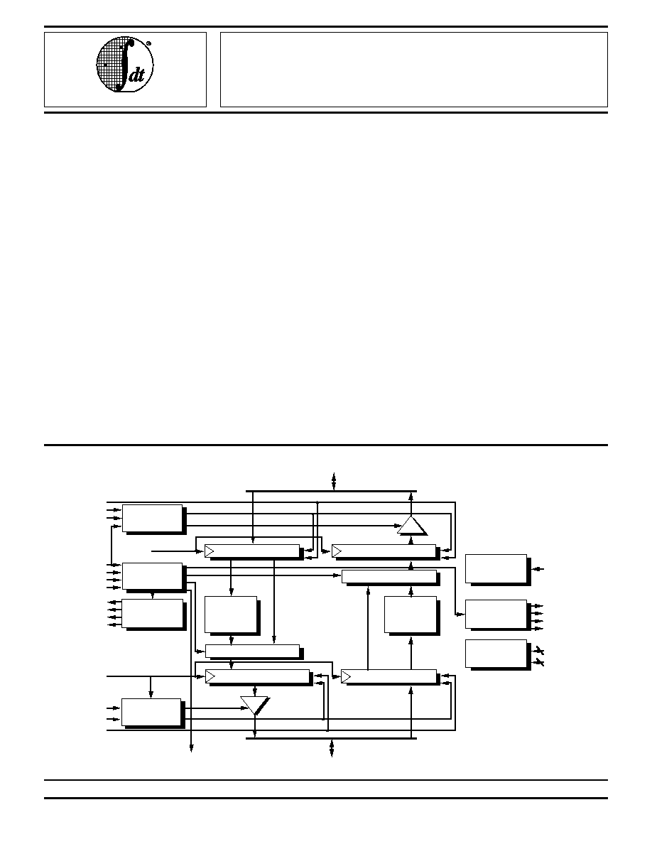
The IDT72605 and IDT72615 are very high-speed, low-
power bidirectional First-In, First-Out (FIFO) memories, with
synchronous interface for fast read and write cycle times. The
SyncBiFIFO
TM
is a data buffer that can store or retrieve
information from two sources simultaneously. Two Dual-Port
FIFO memory arrays are contained in the SyncBiFIFO; one
data buffer for each direction.
The SyncBiFIFO has registers on all inputs and outputs.
Data is only transferred into the I/O registers on clock edges,
hence the interfaces are synchronous. Each Port has its own
independent clock. Data transfers to the I/O registers are
gated by the enable signals. The transfer direction for each
port is controlled independently by a read/write signal. Individ-
ual output enable signals control whether the SyncBiFIFO is
driving the data lines of a port or whether those data lines are
in a high-impedance state.
Bypass control allows data to be directly transferred from
input to output register in either direction.
The SyncBiFIFO has eight flags. The flag pins are full,
empty, almost-full, and almost-empty for both FIFO memo-
ries. The offset depths of the almost-full and almost-empty
flags can be programmed to any location.
The SyncBiFIFO is fabricated using IDT's high-speed,
submicron CMOS technology.
CLK
A
FLAG
LOGIC
MEMORY
ARRAY
512 x 18
256 x 18
INPUT REGISTER
MUX
OUTPUT REGISTER
HIGH
Z
CONTROL
OUTPUT REGISTER
INPUT REGISTER
CLK
B
MUX
MEMORY
ARRAY
512 x 18
256 x 18
HIGH
Z
CONTROL
FLAG
LOGIC
RESET
LOGIC
POWER
SUPPLY
R/
W
A
CS
A
A
2
A
1
A
0
EF
AB
PAE
AB
PAF
AB
FF
AB
OE
B
R/
W
B
EN
B
EN
A
OE
A
RS
EF
BA
PAE
BA
PAF
BA
FF
BA
V
CC
GND
3
BYP
B
µ
P
INTERFACE
7
D
B0
-D
B17
D
A0
-D
A17
2704 drw 01
FUNCTIONAL BLOCK DIAGRAM
For latest information contact IDT's web site at www.idt.com or fax-on-demand at 408-492-8391.
5.18
1
IDT72605/IDT72615 CMOS SyncBiFIFO
256 x 18 x 2 and 512 x 18 x 2
COMMERCIAL TEMPERATURE RANGE
5.18
2
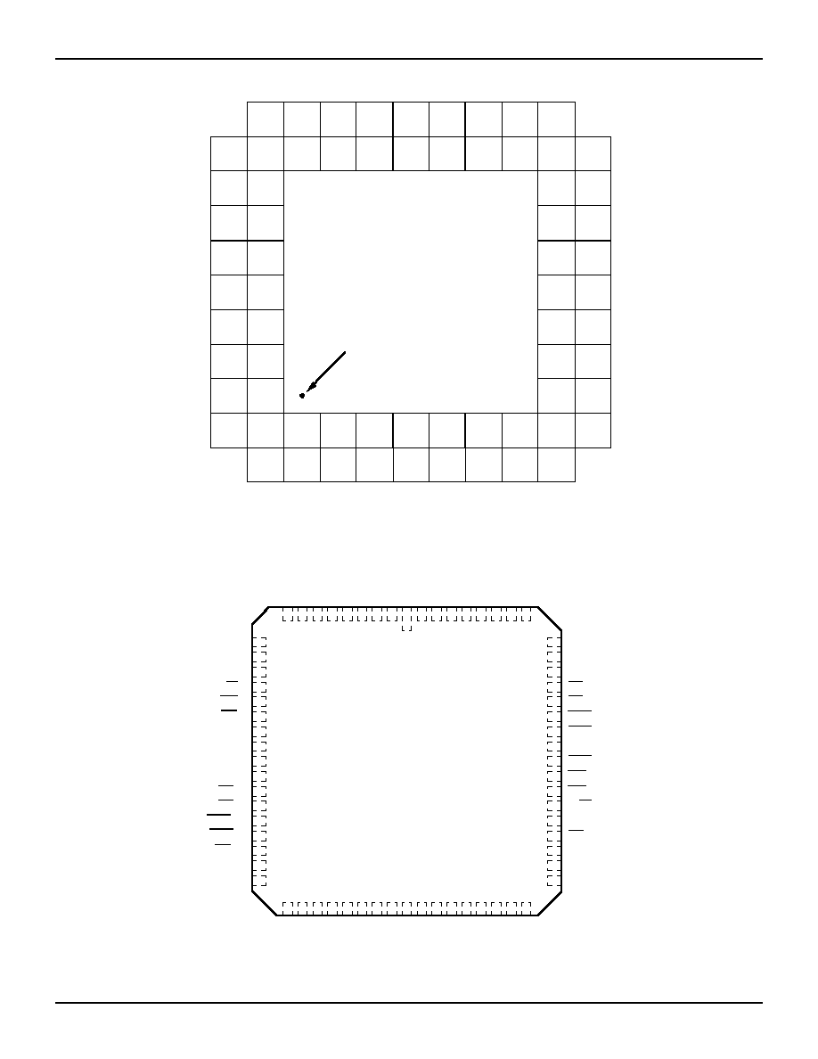
PIN CONFIGURATIONS
PLCC
Top View
GND
GND
D
B16
D
B15
D
B17
PAF
AB
EF
AB
GND
A
2
V
CC
D
A17
GND
D
A16
CLK
A
EN
A
A
0
A
1
A
B
C
D
E
F
G
H
J
K
L
01
02
03
04
05
06
07
08
09
10
11
FF
AB
R/
W
A
Pin 1 Designator
2704 drw 02
GND
D
A15
GND
PAE
AB
CS
A
RS
GND
OE
A
D
B4
D
B5
D
B6
D
B7
D
B8
D
B11
D
B10
D
B9
D
B12
D
B13
D
B14
D
B3
D
B2
D
B1
D
B0
CLK
B
EN
B
BYP
B
FF
BA
PAF
BA
D
A0
D
A1
D
A2
D
A3
D
A4
D
A5
D
A6
D
A7
D
A8
D
A9
D
A10
D
A11
D
A12
D
A13
D
A14
V
CC
R/
W
B
OE
B
PAE
BA
EF
BA
V
CC
G68-1
PGA
Top View
61
62
63
64
65
66
67
68
1
2
3
4
5
6
7
8
9
10
11
18
19
20
21
22
23
24
25
26
17
16
15
14
13
12
52
51
50
49
48
47
46
45
44
53
54
55
56
57
60
59
58
35
43
42
41
40
39
38
37
36
34
33
32
31
30
29
28
27
CLK
B
D
B0
D
B2
D
B1
BYP
B
OE
B
EN
B
R/W
RS
PAF
BA
PAE
BA
FF
BA
EF
BA
GND
D
A2
D
A1
D
A0
B
GND
D
A3
D
A4
GND
D
A15
D
A13
D
A14
D
A12
D
A11
D
A10
V
CC
GND
D
A5
D
A6
D
A7
D
A8
D
A9
D
B9
V
CC
D
B15
GND
D
B8
D
B7
D
B6
D
B14
D
B13
D
B12
D
B11
D
B10
GND
GND
D
B5
D
B4
D
B3
EF
AB
D
B16
D
B17
A
2
V
CC
A
1
D
A16
D
CLK
A
A17
A
0
CS
A
EN
A
R/W
A
FF
AB
PAE
AB
PAF
AB
OE
A
2704 drw 03
J68-1
IDT72605/IDT72615 CMOS SyncBiFIFO
256 x 18 x 2 and 512 x 18 x 2
COMMERCIAL TEMPERATURE RANGE
5.18
3
PIN CONFIGURATIONS
PIN 1
1
2
3
4
5
6
7
8
9
10
11
12
13
14
15
16
DA
1
DA
0
EF
BA
FF
BA
PAE
BA
PAF
BA
GND
BYB
B
OE
B
EN
B
R/
W
B
CLK
B
RS
DB
0
DB
1
DB
2
DB
3
DB
4
GND
DB
5
DB
6
DB
7
DB
8
DB
9
DB
10
DB
11
DB
12
DB
13
DB
14
GND
DB
15
DB
16
48
47
46
45
44
43
42
41
40
39
38
37
36
35
34
33
DA
16
DA
17
CLK
A
R/
W
A
EN
A
CS
A
A
0
A
1
A
2
V
CC
EF
AB
FF
AB
PAE
AB
PAF
AB
OE
A
DB
17
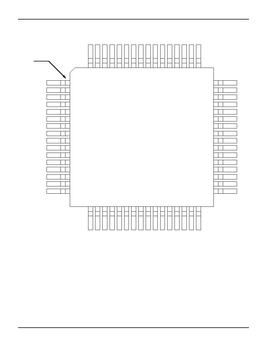
64 63 62 61 60 59 58 57 56 55 54 53 52 51 50 49
17 18 19 20 21 22 23 24 25 26 27 28 29 30 31 32
2704 drw 04
DA
2
DA
3
DA
4
DA
5
DA
6
DA
7
DA
8
DA
9
GND
DA
10
DA
11
DA
12
DA
13
DA
14
DA
15
VCC
PN64-1
TQFP
Top View

IDT72605/IDT72615 CMOS SyncBiFIFO
256 x 18 x 2 and 512 x 18 x 2
COMMERCIAL TEMPERATURE RANGE
5.18
4
PIN DESCRIPTION
Symbol
Name
I/O
Description
D
A0
-D
A17
Data A
I/O
Data inputs & outputs for the 18-bit Port A bus.
CS
A
Chip Select A
I
Port A is accessed when
CS
A
is LOW. Port A is inactive if
CS
A
is HIGH.
R/
W
A
Read/Write A
I
This pin controls the read or write direction of Port A. If R/
W
A
is LOW, Data A input data is
written into Port A. If R/
W
A
is HIGH, Data A output data is read from Port A. In bypass mode,
when R/
W
A
is LOW, message is written into A
B output register. If R/
W
A
is HIGH, message
is read from B
A output register.
CLK
A
Clock A
I
CLK
A
is typically a free running clock. Data is read or written into Port A on the rising edge of
CLK
A
.
EN
A
Enable A
I
When
EN
A
is LOW, data can be read or written to Port A. When
EN
A
is HIGH, no data
transfers occur.
OE
A
Output Enable A
I
When R/
W
A
is HIGH , Port A is an output bus and
OE
A
controls the high-impedance state of
D
A0
-D
A17
. If
OE
A
is HIGH, Port A is in a high-impedance state. If
OE
A
is LOW while
CS
A
is
LOW and R/
W
A
is HIGH, Port A is in an active (low-impedance) state.
A
0
, A
1
, A
2
Addresses
I
When
CS
A
is asserted, A
0
, A
1
, A
2
and R/
W
A
are used to select one of six internal resources.
D
B0
-D
B17
Data B
I/O
Data inputs & outputs for the 18-bit Port B bus.
R/
W
B
Read/Write B
I
This pin controls the read or write direction of Port B. If R/
W
B
is LOW, Data B input data is
written into Port B. If R/
W
B
is HIGH, Data B output data is read from Port B. In bypass mode,
when R/
W
B
is LOW, message is written into B
A output register. If R/
W
B
is HIGH, message
is read from A
B output register.
CLK
B
Clock B
I
Clock B is typically a free running clock. Data is read or written into Port B on the rising edge
of CLK
B
.
EN
B
Enable B
I
When
EN
B
is LOW, data can be read or written to Port B. When
EN
B
is HIGH, no data
transfers occur.
OE
B
Output Enable B
I
When R/
W
B
is HIGH , Port B is an output bus and
OE
B
controls the high-impedance state of
D
B0
-D
B17
. If OE
B
is HIGH, Port B is in a high-impedance state. If
OE
B
is LOW while R/
W
B
is HIGH, Port B is in an active (low-impedance) state.
EF
AB
A
B Empty Flag
O
When
EF
AB
is LOW, the A
B FIFO is empty and further data reads from Port B are inhibited.
When
EF
AB
is HIGH, the FIFO is not empty.
EF
AB
is synchronized to CLK
B
. In the bypass
mode,
EF
AB
HIGH indicates that data D
A0
-D
A17
is available for passing through. After the
data D
B0
-D
B17
has been read,
EF
AB
goes LOW.
PAE
AB
A
B
O
When
PAE
AB
is LOW, the A
B FIFO is almost empty. An almost empty FIFO contains less
Programmable
than or equal to the offset programmed into
PAE
AB
Register. When
PAE
AB
is HIGH, the
Almost-Empty Flag
A
B FIFO contains more than offset in
PAE
AB
Register. The default offset value for
PAE
AB
Register is 8.
PAE
AB
is synchronized to CLK
B
.
PAF
AB
A
B
O
When
PAF
AB
is LOW, the A
B FIFO is almost full. An almost full FIFO contains greater than
Programmable
the FIFO depth minus the offset programmed into
PAF
AB
Register. When PAF
AB
is HIGH,
Almost-Full Flag
the A
B FIFO contains less than or equal to the depth minus the offset in PAF
AB
Register.
The default offset value for PAF
AB
Register is 8.
PAF
AB
is synchronized to CLK
A
.
FF
AB
A
B Full Flag
O
When
FF
AB
is LOW, the A
B FIFO is full and further data writes into Port A are inhibited.
When
FF
AB
is HIGH, the FIFO is not full.
FF
AB
is synchronized to CLK
A
. In bypass mode,
FF
AB
tells Port A that a message is waiting in Port B's output register. If
FF
AB
is LOW, a
bypass message is in the register. If
FF
AB
is HIGH, Port B has read the message and another
message can be written into Port A.
EF
BA
B
A Empty Flag
O
When
EF
BA
is LOW, the B
A FIFO is empty and further data reads from Port A are inhibited.
When
EF
BA
is HIGH, the FIFO is not empty.
EF
BA
is synchronized to CLK
A
. In the bypass
mode,
EF
BA
HIGH indicates that data D
B0
-D
B17
is available for passing through. After the
data D
A0
-D
A17
has been read,
EF
BA
goes LOW on the following cycle.
PAE
BA
B
A
O
When
PAE
BA
is LOW, the B
A FIFO is almost empty. An almost empty FIFO contains less
Programmable
than or equal to the offset programmed into
PAE
BA
Register. When
PAE
BA
is HIGH, the
Almost-Empty Flag
B
A FIFO contains more than offset in
PAE
BA
Register. The default offset value for
PAE
BA
Register is 8.
PAE
BA
is synchronized to CLK
A
.
PAF
BA
B
A
O
When
PAF
BA
is LOW, the B
A FIFO is almost full. An almost full FIFO contains greater than
Programmable
the FIFO depth minus the offset programmed into
PAF
BA
Register. When
PAF
BA
is HIGH,
Almost-Full Flag
the B
A FIFO contains less than or equal to the depth minus the offset in
PAF
BA
Register.
The default offset value for
PAF
BA
Register is 8.
PAF
BA
is synchronized to CLK
B
.
2704 tbl 01

IDT72605/IDT72615 CMOS SyncBiFIFO
256 x 18 x 2 and 512 x 18 x 2
COMMERCIAL TEMPERATURE RANGE
5.18
5
RECOMMENDED DC
OPERATING CONDITIONS
Symbol
Parameter
Min. Typ. Max. Unit
V
CC
Supply Voltage
4.5
5.0
5.5
V
GND
Supply Voltage
0
0
0
V
V
IH
Input High Voltage
2.0
--
--
V
V
IL
(1)
Input Low Voltage
--
--
0.8
V
NOTE:
2704 tbl 04
1. 1.5V undershoots are allowed for 10ns once per cycle.
PIN DESCRIPTION (Continued)
Symbol
Name
I/O
Description
2704 tbl 02
FF
BA
B
A Full Flag
O
When
FF
BA
is LOW, the B
A FIFO is full and further data writes into Port B are inhibited.
When
FF
BA
is HIGH, the FIFO is not full.
FF
BA
is synchronized to CLK
B
. In bypass mode,
FF
BA
tells Port B that a message is waiting in Port A's output register. If
FF
BA
is LOW, a
bypass message is in the register. If
FF
BA
is HIGH, Port A has read the message and another
message can be written into Port B.
BYP
B
Port B Bypass
O
This flag informs Port B that the Synchronous BiFIFO is in bypass mode. When BYP
B
is
Flag
LOW, Port A has placed the FIFO into bypass mode. If
BYP
B
is HIGH, the Synchronous
BiFIFO passes data into memory.
BYP
B
is synchronized to CLK
B
.
RS
Reset
I
A LOW on this pin will perform a reset of all Synchronous BiFIFO functions.
V
CC
Power
There are three +5V power pins for the PLCC and PGA packages and two for the TQFP.
GND
Ground
There are seven ground pins for the PLCC and PGA packages and four for the TQFP.
ABSOLUTE MAXIMUM RATINGS
(1)
Symbol
Rating
Com'l.
Mil.
Unit
V
TERM
Terminal Voltage
≠0.5 to +7.0
≠0.5 to +7.0
V
with Respect
to Ground
T
A
Operating
0 to +70
≠55 to +125
∞
C
Temperature
T
BIAS
Temperature
≠55 to +125
≠65 to +135
∞
C
Under Bias
T
STG
Storage
≠55 to +125
≠65 to +150
∞
C
Temperature
I
OUT
DC Output Current
50
50
mA
NOTE:
2704 tbl 03
1. Stresses greater than those listed under ABSOLUTE MAXIMUM RAT-
INGS may cause permanent damage to the device. This is a stress rating
only and functional operation of the device at these or any other conditions
above those indicated in the operational sections of this specification is not
implied. Exposure to absolute maximum rating conditions for extended
periods may affect reliability.
2704 tbl 05
CAPACITANCE
(T
A
= +25
∞
C, F = 1.0MHz)
Symbol
Parameter
Conditions
Max.
Unit
C
IN
(2)
Input Capacitance
V
IN
= 0V
10
pF
C
OUT
(1,2)
Output Capacitance
V
OUT
= 0V
10
pF
NOTES:
1. With output deselected.
2. Characterized values, not currently tested.
2704 tbl 06
DC ELECTRICAL CHARACTERISTICS
(Commercial: V
CC
= 5V
±
10%, T
A
= 0
∞
C to +70
∞
C)
IDT72615L
IDT72605L
Commercial
t
CLK
= 20, 25, 35, 50ns
Symbol
Parameter
Min.
Typ.
Max.
Unit
I
IL
(1)
Input Leakage Current (Any Input)
≠1
--
1
µ
A
I
OL
(2)
Output Leakage Current
≠10
--
10
µ
A
V
OH
Output Logic "1" Voltage I
OUT
= ≠2mA
2.4
--
--
V
V
OL
Output Logic "0" Voltage I
OUT
= 8mA
--
--
0.4
V
I
CC
(3)
Average V
CC
Power Supply Current
--
--
230
mA
NOTES:
1. Measurements with 0.4V
V
IN
V
CC
.
2.
OEA
,
OEB
V
IH
; 0.4
V
OUT
V
CC
.
3. Tested with outputs open. Testing frequency f=20MHz