1 of 46
March 26, 2001
2001 Integrated Device Technology, Inc.
DSC 5347/7
Data Path Interface (DPI) to
UTOPIA Level 1 Header
Translation Device
)
)
)
)H
H
H
HD
D
D
DWX
WX
WX
WXUUUUHV
HV
HV
HV /
/
/
/LVW
LVW
LVW
LVW
8, 12, 24, 28 or 32-bit ATM header lookup. Ideal for network
side of SwitchStar DSLAM designs where full header access
is needed
Supports VPI Tunneling
Supports both UNI and NNI formats
Accounting functionality counts the number of cells on a
per VC basis
8-bit UTOPIA Level 1 Tx and Rx interfaces
Supports UTOPIA Level 1 cell mode operation
4-bit DPI Tx and Rx interfaces
DPI interface supports cell sizes from 52 to 56 bytes for
applications requiring a TAG
DPI interface operates up to 66MHz
In-StreamTM (In-band) programming for configuration of the
77V012, PHY and external search SRAM
Supports up to 8K active connections with an external 128K
x 32 SRAM. Up to 16K connections are supported in a 256K
x 32 SRAM
Inserts new ATM cell header and up to four bytes of TAG in
receive direction, and removes TAG from cell header in
transmit direction
Utility bus interface for programming PHY devices
Single +3.3V � 0.3V power supply required
Inputs are +5.0V tolerant
'HVFULSWLRQ
The IDT77V012 provides full header translation functionality along
with Data Path Interface (DPI) to UTOPIA Level 1 translation for switch
and DSLAM designs using the IDT SwitchStar. The address search and
replacement algorithm is performed using a VPI Tunneling or Full
Header format on 8, 12, 24, 28 or 32-bits of the header. This added flex-
ibility makes it suitable for both UNI and NNI formats. External memory
is required to perform the header translation (receive direction only),
which will support up to 16K connections using a 256K x 32 SRAM. The
new header, which is obtained as a result of the search, can be used to
overwrite the existing cell header in the receive path. A four byte TAG
can also be added to aid in routing cells.
The 77V012 also contains cell counters in the transmit and receive
direction. The counters can be used to provide detailed per VC
accounting information for a particular port.
Other features include In-StreamTM programming, which can be
utilized on either the DPI or UTOPIA interfaces, a Utility Bus interface for
accessing registers in the PHY device, and an interface for an
EEPROM.
%OR
%OR
%OR
%ORF
F
F
FN 'L
N 'L
N 'L
N 'LDJU
DJU
DJU
DJUD
D
D
DP
P
P
P
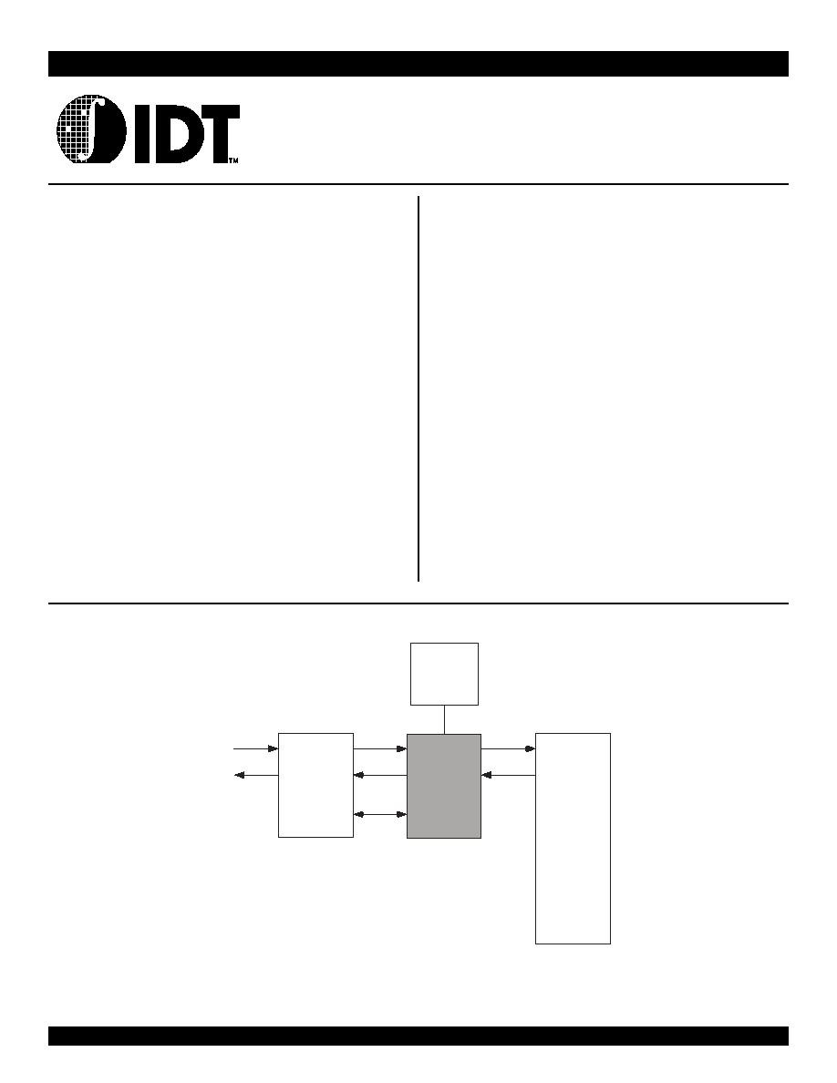
Figure 1 Typical IDT77V012 Application with the IDT77V400 Switching Memory
OC-3
or
STS-3
IDT77155
PHY
IDT77V012
UTOPIA 1
to DPI
interface w/
Header
Translation
IDT77V400
Switching
Memory
UTOPIA 1
Receive
UTOPIA 1
Transmit
Utility
Bus
DPI
Receive
DPI
Transmit
"
"
"
"
"
"
"
"
5347drw01
SRAM
64K x 32
to
256K x 32
IDT77V012
2 of 46
March 26, 2001
IDT77V012
%OR
%OR
%OR
%ORF
F
F
FN 'L
N 'L
N 'L
N 'LDJU
DJU
DJU
DJUD
D
D
DP
P
P
P
3LQ &RQILJX
3LQ &RQILJX
3LQ &RQILJX
3LQ &RQILJXUUUUDWLRQ
DWLRQ
DWLRQ
DWLRQ
Note: 1. All power pins must be connected to a 3.3V � 0.3V power supply.
2. All GND pins must be connected to ground supply.
3. This text does not indicate orientation of the actual part-marking.
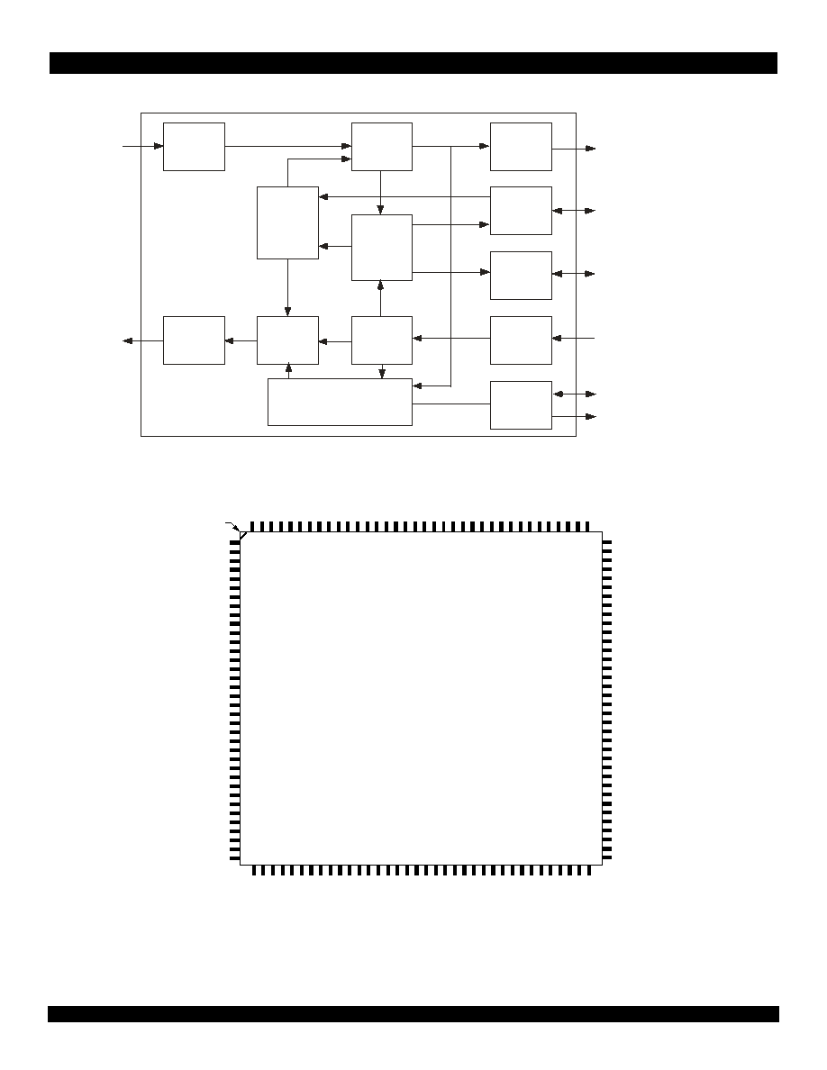
UTOPIA 1
Transmit
Interface
EEPROM
Interface
Utility Bus
Interface
UTOPIA 1
Receive
Interface
DPI
Transmit
Interface
DPI
Receive
Interface
TAG
Removal
Cell
Receiver
Cell
Generator
TAG
Adder and
MUX
Search Tree
RxFIFO
SRAM
Interface
5347drw02
INDEX
DTxDATA[0]
DTxFRM
DTxDATA[1]
DTxDATA[2]
DTxDATA[3]
VCC
IDT77V012
PQFP
TOP
VIEW
(3)
8
9
10
11
12
13
14
15
16
1
2
3
4
5
6
7
17
18
19
20
22
23
24
25
26
27
28
29
30
31
32
33
34
35
36
21
GND
VCC
GND
DTxCLK
4
8
4
7
4
6
4
5
4
4
4
3
4
2
4
1
4
0
3
9
3
8
3
7
4
9
5
0
5
1
5
2
5
3
5
4
5
5
5
6
5
7
5
8
5
9
6
0
6
1
6
2
6
3
6
4
6
5
6
6
6
7
6
8
6
9
7
0
7
1
7
2
V
C
C
D
A
T
A
[
1
0
]
D
A
T
A
[
1
1
]
D
A
T
A
[
1
2
]
D
A
T
A
[
1
3
]
D
A
T
A
[
1
4
]
D
A
T
A
[
1
5
]
A
D
D
R
[
1
6
]
G
N
D
V
C
C
A
D
D
R
[
1
5
]
A
D
D
R
[
1
4
]
A
D
D
R
[
1
3
]
A
D
D
R
[
1
2
]
A
D
D
R
[
1
1
]
A
D
D
R
[
1
0
]
A
D
D
R
[
9
]
A
D
D
R
[
8
]
A
D
S
P
O
E
G
W
S
C
L
K
G
N
D
V
C
C
C
E
A
D
D
R
[
0
]
A
D
D
R
[
1
]
A
D
D
R
[
2
]
A
D
D
R
[
3
]
A
D
D
R
[
4
]
A
D
D
R
[
5
]
A
D
D
R
[
6
]
A
D
D
R
[
7
]
D
A
T
A
[
1
6
]
G
N
D
GND
GND
DRxFRM
DRxDATA[0]
DRxDATA[1]
DRxDATA[2]
DRxDATA[3]
VCC
DRxCLK
E E C S
EEDIN
EEDOUT
EECLK
DATA[0]
DATA[1]
DATA[2]
GND
DATA[3]
DATA[4]
DATA[5]
DATA[6]
DATA[7]
DATA[8]
DATA[9]
GND
101
100
99
98
97
96
95
94
93
108
107
106
105
104
103
102
92
91
90
89
87
86
85
84
83
82
81
80
79
78
77
76
75
74
73
88
VCC
CNTRL_B
ALE
AD[7]
AD[6]
AD[5]
AD[4]
AD[3]
GND
AD[2]
AD[1]
AD[0]
PHYIN T
R D
W R
PH YR ST
PH Y C S
DATA[31]
DATA[30]
DATA[29]
DATA[28]
DATA[27]
DATA[26]
DATA[25]
DATA[24]
DATA[23]
GND
DATA[22]
DATA[21]
DATA[20]
DATA[19]
DATA[18]
DATA[17]
1
3
3
1
3
4
1
3
5
1
3
6
1
3
7
1
3
8
1
3
9
1
4
0
1
4
1
1
4
2
1
4
3
1
4
4
1
3
2
1
3
1
1
3
0
1
2
9
1
2
8
1
2
7
1
2
6
1
2
5
1
2
4
1
2
3
1
2
2
1
2
1
1
2
0
1
1
9
1
1
8
1
1
7
1
1
6
1
1
5
1
1
4
1
1
3
1
1
2
1
1
1
1
1
0
1
0
9
V
C
C
G
N
D
V
C
C
G
N
D
V
C
C
T
S
O
C
C
N
T
R
L
_
A
G
N
D
T
x
P
R
T
Y
T
x
D
A
T
A
[
7
]
T
x
D
A
T
A
[
6
]
T
x
D
A
T
A
[
5
]
T
x
D
A
T
A
[
4
]
T
x
D
A
T
A
[
3
]
T
x
D
A
T
A
[
2
]
T
x
D
A
T
A
[
1
]
T
x
D
A
T
A
[
0
]
T
C
L
A
V
T
E
N
B
T
C
L
K
T
x
L
E
D
R
S
O
C
R
x
D
A
T
A
[
7
]
R
x
D
A
T
A
[
6
]
R
x
D
A
T
A
[
5
]
R
x
D
A
T
A
[
4
]
R
x
D
A
T
A
[
3
]
V
C
C
G
N
D
R
x
L
E
D
R
C
L
K
R
E
N
B
R
C
L
A
V
R
x
D
A
T
A
[
0
]
R
x
D
A
T
A
[
1
]
R
x
D
A
T
A
[
2
]
5347drw03
SYS RST
SYSCLK
VCC
VCC
A
D
D
R
[
1
7
]

3 of 46
March 26, 2001
IDT77V012
3LQ 'HVFULSWL
3LQ 'HVFULSWL
3LQ 'HVFULSWL
3LQ 'HVFULSWLR
R
R
RQ
Q
Q
Q 7
7
7
7D
D
D
DEOH
EOH
EOH
EOH
3LQ
1DPH
3LQ
1XPEHU
,QSXW
2XWSXW
'HVFULSWLRQ
DRxDATA [0]
11
O
4-bit output data bus used to transfer data to a DPI device [LSB].
DRxDATA [1]
12
O
4-bit output data bus used to transfer data to a DPI device [LSB+1].
DRxDATA [2]
13
O
4-bit output data bus used to transfer data to a DPI device [LSB+2].
DRxDATA [3]
14
O
4-bit output data bus used to transfer data to a DPI device [MSB].
DRxFRM
10
O
DPI receive start of frame marker.
DRxCLK
17
I/O
Receive DPI clock.
DTxDATA [0]
2
I
4-bit input data bus used to transfer data from a DPI device [LSB].
DTxDATA [1]
3
I
4-bit input data bus used to transfer data from a DPI device [LSB+1].
DTxDATA [2]
4
I
4-bit input data bus used to transfer data from a DPI device [LSB+2].
DTxDATA [3]
5
I
4-bit input data bus used to transfer data from a DPI device [MSB].
DTxFRM
6
I
DPI transmit start of frame marker.
DTxCLK
9
O
Transmit DPI clock.
RxDATA [0]
138
I
8-bit UTOPIA 1 input data bus used to transfer data from a PHY device [LSB].
RxDATA [1]
137
I
8-bit UTOPIA 1 input data bus used to transfer data from a PHY device [LSB+1].
RxDATA [2]
136
I
8-bit UTOPIA 1 input data bus used to transfer data from a PHY device [LSB+2].
RxDATA [3]
134
I
8-bit UTOPIA 1 input data bus used to transfer data from a PHY device [LSB+3].
RxDATA [4]
133
I
8-bit UTOPIA 1 input data bus used to transfer data from a PHY device [LSB+4].
RxDATA [5]
132
I
8-bit UTOPIA 1 input data bus used to transfer data from a PHY device [LSB+5].
RxDATA [6]
131
I
8-bit UTOPIA 1 input data bus used to transfer data from a PHY device [LSB+6].
RxDATA [7]
130
I
8-bit UTOPIA 1 input data bus used to transfer data from a PHY device [MSB].
RSOC
129
I
UTOPIA 1 Receive Start of Cell.
RCLAV
139
I
UTOPIA 1 Receive Cell Available.
RENB
141
O
UTOPIA 1 Receive Enable.
RxLED
142
O
UTOPIA 1 Receive LED, open drain.
RCLK
143
O
UTOPIA 1 Receive Clock.
TxDATA [0]
122
O
8-bit UTOPIA 1 output data bus used to transfer data to a PHY device [LSB].
TxDATA [1]
121
O
8-bit UTOPIA 1 output data bus used to transfer data to a PHY device [LSB+1].
TxDATA [2]
120
O
8-bit UTOPIA 1 output data bus used to transfer data to a PHY device [LSB+2].
TxDATA [3]
119
O
8-bit UTOPIA 1 output data bus used to transfer data to a PHY device [LSB+3].
TxDATA [4]
118
O
8-bit UTOPIA 1 output data bus used to transfer data to a PHY device [LSB+4].
TxDATA [5]
115
O
8-bit UTOPIA 1 output data bus used to transfer data to a PHY device [LSB+5].
TxDATA [6]
114
O
8-bit UTOPIA 1 output data bus used to transfer data to a PHY device [LSB+6].
TxDATA [7]
113
O
8-bit UTOPIA 1 output data bus used to transfer data to a PHY device [MSB].
TSOC
111
O
UTOPIA 1 Transmit Start of Cell.
Table 1 Pin Description (Part 1 of 4)

4 of 46
March 26, 2001
IDT77V012
TCLAV
128
I
UTOPIA 1 Transmit Cell Available.
TENB
123
O
UTOPIA 1 Transmit Enable.
TxLED
124
O
UTOPIA 1 Transmit LED, open drain.
TCLK
125
O
UTOPIA 1 Transmit Clock.
TxPRTY
112
O
Transmit Parity.
EECLK
21
O
EEPROM Clock.
EECS
18
O
EEPROM Chip Select.
EEDIN
19
I
Serial input from the EEPROM.
EEDOUT
20
O
Serial output to the EEPROM.
AD[0]
96
I/O
Utility Bus Address and Data Bus [LSB].
AD[1]
97
I/O
Utility Bus Address and Data Bus [LSB+1].
AD[2]
98
I/O
Utility Bus Address and Data Bus [LSB+2].
AD[3]
101
I/O
Utility Bus Address and Data Bus [LSB+3].
AD[4]
102
I/O
Utility Bus Address and Data Bus [LSB+4].
AD[5]
103
I/O
Utility Bus Address and Data Bus [LSB+5].
AD[6]
104
I/O
Utility Bus Address and Data Bus [LSB+6].
AD[7]
105
I/O
Utility Bus Address and Data Bus [MSB].
PHYCS
91
O
Utility Bus PHY Chip Select.
RD
94
O
Utility Bus Read.
WR
93
O
Utility Bus Write.
ALE
106
O
Utility Bus Address Latch Enable.
PHYRST
92
O
PHY Reset, open drain.
PHYINT
95
I
PHY Interrupt.
SYSRST
22
I
System Reset.
SYSCLK
23
I
System Clock.
CNTRL_A
110
O
Control pin A.
CNTRL_B
107
O
Control pin B.
SCLK
58
O
SRAM Clock.
ADSP
55
O
SRAM Address Status Processor.
GW
57
O
SRAM Global Write Enable.
CE
62
O
SRAM Chip Enable.
OE
56
O
SRAM Output Enable.
ADDR[0]
63
O
SRAM Address bus.
I
Tx TAG Size [0]. Number of bytes to remove from cell in transmit direction (LSB).
3LQ
1DPH
3LQ
1XPEHU
,QSXW
2XWSXW
'HVFULSWLRQ
Table 1 Pin Description (Part 2 of 4)

5 of 46
March 26, 2001
IDT77V012
ADDR[1]
64
O
SRAM Address bus.
I
Tx TAG Size [1]. Number of bytes to remove from cell in transmit direction (LSB+1).
ADDR[2]
65
O
SRAM Address bus.
I
Tx TAG Size [2]. Number of bytes to remove from cell in transmit direction (MSB).
ADDR[3]
66
O
SRAM Address bus.
I
"Tx TAG Location. Location of TAG in the transmit direction. "0" beginning of cell, "1" end of cell."
ADDR[4]
67
O
SRAM Address bus.
I
"Tx Add HEC. Add a HEC placeholder. "0" do not add placeholder, "1" add placeholder."
ADDR[5]
68
O
SRAM Address bus.
I
Rx TAG Size [0]. Number of bytes to add to cell in receive direction (LSB).
ADDR[6]
69
O
SRAM Address bus.
I
Rx TAG Size [1]. Number of bytes to add to cell in receive direction (LSB + 1).
ADDR[7]
70
O
SRAM Address bus.
I
Rx TAG Size [2]. Number of bytes to add to cell in receive direction (MSB).
ADDR[8]
54
O
SRAM Address bus.
I
"Rx Rem HEC. Remove HEC from the cell. "0" do not remove the HEC byte, "1" remove the HEC byte."
ADDR[9]
53
O
SRAM Address bus.
I
"DPI Mode. Selects DRxCLK direction. "0" switch mode (output), "1" normal mode (input)."
ADDR[10]
52
O
SRAM Address bus.
I
"In-StreamTM Direction. Selects the interface that the In-StreamTM cells will be filtered on. "0" transmit DPI inter-
face, "1" receive UTOPIA interface."
ADDR[11]
51
O
SRAM Address bus.
I
"Init from EEPROM. Selects whether first four bytes stored in EEPROM are to be written to In-StreamTM Cell
Header registers. "0" do not write value to registers, "1" write four byte value from EEPROM to In-StreamTM Cell
Header registers."
ADDR[12]
50
O
SRAM Address bus.
ADDR[13]
49
O
SRAM Address bus.
ADDR[14]
48
O
SRAM Address bus.
ADDR[15]
47
O
SRAM Address bus.
ADDR[16]
44
O
SRAM Address bus.
ADDR[17]
61
O
SRAM Address bus.
DATA[0]
26
I/O
SRAM Data bus.
DATA[1]
27
I/O
SRAM Data bus.
DATA[2]
28
I/O
SRAM Data bus.
DATA[3]
29
I/O
SRAM Data bus.
DATA[4]
30
I/O
SRAM Data bus.
3LQ
1DPH
3LQ
1XPEHU
,QSXW
2XWSXW
'HVFULSWLRQ
Table 1 Pin Description (Part 3 of 4)

6 of 46
March 26, 2001
IDT77V012
DATA[5]
31
I/O
SRAM Data bus.
DATA[6]
32
I/O
SRAM Data bus.
DATA[7]
33
I/O
SRAM Data bus.
DATA[8]
34
I/O
SRAM Data bus.
DATA[9]
35
I/O
SRAM Data bus.
DATA[10]
38
I/O
SRAM Data bus.
DATA[11]
39
I/O
SRAM Data bus.
DATA[12]
40
I/O
SRAM Data bus.
DATA[13]
41
I/O
SRAM Data bus.
DATA[14]
42
I/O
SRAM Data bus.
DATA[15]
43
I/O
SRAM Data bus.
DATA[16]
71
I/O
SRAM Data bus.
DATA[17]
74
I/O
SRAM Data bus.
DATA[18]
75
I/O
SRAM Data bus.
DATA[19]
76
I/O
SRAM Data bus.
DATA[20]
77
I/O
SRAM Data bus.
DATA[21]
78
I/O
SRAM Data bus.
DATA[22]
79
I/O
SRAM Data bus.
DATA[23]
82
I/O
SRAM Data bus.
DATA[24]
83
I/O
SRAM Data bus.
DATA[25]
84
I/O
SRAM Data bus.
DATA[26]
85
I/O
SRAM Data bus.
DATA[27]
86
I/O
SRAM Data bus.
DATA[28]
87
I/O
SRAM Data bus.
DATA[29]
88
I/O
SRAM Data bus.
DATA[30]
89
I/O
SRAM Data bus.
DATA[31]
90
I/O
SRAM Data bus.
Vcc
7,15,25,37,
46,60,73,80,
100,109,116,
127,135
Power
3.3V Power supply pins.
GND
1,8,16,24,36,
45,59,72,81,
99,108,117,
126,140,144
Ground
Ground pins.
3LQ
1DPH
3LQ
1XPEHU
,QSXW
2XWSXW
'HVFULSWLRQ
Table 1 Pin Description (Part 4 of 4)

7 of 46
March 26, 2001
IDT77V012
$EVROXWH 0D
$EVROXWH 0D
$EVROXWH 0D
$EVROXWH 0D[
[
[
[LPXP
LPXP
LPXP
LPXP 5
5
5
5D
D
D
DWLQJV
WLQJV
WLQJV
WLQJV
5
5
5
5H
H
H
HFRPPHQGHG
FRPPHQGHG
FRPPHQGHG
FRPPHQGHG 2
2
2
2SH
SH
SH
SHUUUUD
D
D
DWLQJ &RQGLWL
WLQJ &RQGLWL
WLQJ &RQGLWL
WLQJ &RQGLWLR
R
R
RQV
QV
QV
QV
'& (OHFWULFDO
'& (OHFWULFDO
'& (OHFWULFDO
'& (OHFWULFDO &KDU
&KDU
&KDU
&KDUDFWHULVWLFV
DFWHULVWLFV
DFWHULVWLFV
DFWHULVWLFV
&D
&D
&D
&DS
S
S
SDFLWDQFH
DFLWDQFH
DFLWDQFH
DFLWDQFH
6\PERO
3DUDPHWHU
0LQ
0D[
8QLW
V
CC
3.3V Digital Supply Voltage
G
ND
-0.3
3.6
V
V
IN
Digital Input Voltage
G
ND
-0.3
5.50
V
V
OUT
Digital Output Voltage
Gv-0.3
V
CC
V
G
ND
Digital Ground Voltage
0
0
V
I
OUT1
Output Current CNTRL_A, CNTRL_B
--
12.0
mA
I
OUT2
Output Current EECLK, EECS, EEDOUT
--
2.0
mA
I
OUT3
Output Current RxLED, TxLED, PHYRST (open drain)
--
6.0
mA
I
OUT4
Output Current all outputs except those listed in I
OUT1
, I
OUT2
and I
OUT3
--
6.0
mA
T
STG
Storage Temperature
-55
140
C�
6\PERO
3DUDPHWHU
0LQ
0D[
8QLW
V
CC
Digital Supply Voltage
3.0
3.6
V
V
IN
TTL Input Voltage
GND
5.5
V
T
A
Industrial Operating Temperature
-40
+85
�C
titr
Input TTL rise time
--
2
ns
titf
Input TTL fall time
--
2
ns
V
IH
TTL Input High Voltage
2.0
--
V
V
IL
TTL Input Low Voltage
--
0.8
V
6\PERO
3DUDPHWHU
7HVW &RQGLWLRQV
0LQ
0D[
8QLW
|I
LI
|
Input Leakage Current
V
CC
= 3.3V, V
IN
= 0V to V
CC
10
10
� A
|I
LO
|
Output Leakage Current
V
OUT
= 0V to V
CC
10
10
� A
V
OH
TTL Output High Voltage
I
OH
= -4mA
2.4
--
V
V
OL
TTL Output Low Voltage
I
OL
= +4mA
--
0.4
V
I
CC
Power Supply Current
155.52 Mbps
--
80
mA
6\PERO
3DUDPHWHU
0LQ
7\S
0D[
8QLW
C
IN
Input Capacitance
All Inputs
--
4
--
pF
C
OUT
Output Capacitance
All Outputs
--
6
--
pF
C
BID
Bi-Directional Capacitance
All Bi-directional Pins
--
10
--
pF
8 of 46
March 26, 2001
IDT77V012
'
'
'
'H
H
H
HYLFH ,QWHUIDFH
YLFH ,QWHUIDFH
YLFH ,QWHUIDFH
YLFH ,QWHUIDFH
The 77V012 uses a UTOPIA level 1 interface to receive and transmit
ATM cells to and from the PHY device. It has a UTOPIA master interface
and operates with a 8-bit data bus. UTOPIA cell level handshake is used
to transfer the cells between the ATM layer and the PHY layer. UTOPIA
byte level handshake is not supported by the 77V012.
The Data Path Interface (DPI) uses a 4-bit data bus, which interfaces
the 77V012 to the IDT SwitchStar.
The EEPROM holds information for initialization and Discovery/Iden-
tify cells. The EEPROM is an option and does not need to be imple-
mented.
The Utility Bus interface contains the control pins used to program
and read the internal PHY registers.
The SRAM interface is used to configure internal registers at reset
and to interface with the external SRAM during normal operation.
The Misc. interface offers two test pins, that are controlled through
registers.
87
87
87
872
2
2
23,$
3,$
3,$
3,$ 5
5
5
5H
H
H
HFHL
FHL
FHL
FHLYYYYH
H
H
H ,QWHU
,QWHU
,QWHU
,QWHUIIIIDF
DF
DF
DFH
H
H
H 2SH
2SH
2SH
2SHUUUUD
D
D
DWLRQ
WLRQ
WLRQ
WLRQ
The 77V012 offers a fully compliant UTOPIA Level 1 Receive inter-
face, as specified by the UTOPIA Level 1 specification. The interface is
a UTOPIA master that operates with a 8-bit Input Data Bus
(RxDATA[7:0]). UTOPIA cell level handshake is used to receive ATM
cells from the PHY device. The other signals associated with this inter-
face are Receive Start of Cell (RSOC), Receive Enable (
RENB),
Receive Cell Available (RCLAV), Receive LED (
RxLED), and Receive
Clock (RCLK).
RCLK is a continuous clock, which is half the frequency of System
Clock (SYSCLK).
RxLED indicates if there is activity on the UTOPIA receive bus. This
open drain signal asserts low when a cell is transferred over the bus,
and will stay asserted for 2
22
RCLK cycles. At 40MHz this is approxi-
mately 0.1 seconds.
The 77V012 will assert
RENB low upon detection of a high RCLAV.
Once RSOC is detected the 77V012 will receive the entire cell without
interruption.
When a TAG is not being used there is no delay between back to
back cells. There is a maximum delay of eight clock cycles between
back to back cells when a four byte TAG is being used.
Figure 2 77V012 Interfaces
DRxFRM
DRxCLK
DRxDATA[3:0]
DTxFRM
DTxCLK
DTxDATA[3:0]
RSOC
RCLK
RxDATA[7:0]
R E N B
RCLAV
TSOC
TCLK
TxDATA[7:0]
T E N B
TCLAV
E E C S
EECLK
SCLK
G W
5347drw04
IDT77V012
EEDOUT
DPI
Receive
Interface
DPI
Transmit
Interface
EEDIN
Serial
EEPROM
Interface
S Y S RS T
SYSCLK
System
Interface
A DS P
O E
C E
SRAM
Interface
UTOPIA
Transmit
Interface
UTOPIA
Receive
Interface
ALE
R D
W R
P H Y R S T
P HYI NT
AD[7:0]
Utility Bus
Interface
P HY C S
DATA[31:0]
ADDR[17:0]
TxPRTY
CNTRL_A
CNTRL_B
Misc.
Interface
Rx LE D
T x LED

9 of 46
March 26, 2001
IDT77V012
Cells can be dropped on the Rx UTOPIA interface by setting the
RxData Cell Filter bit of the Configuration 2 register. This option is to
prevent cells from reaching the switch when the 77V012 is in software
reset, but the rest of the system is still under normal operation. When
this bit is set to a one the 77V012 will drop all data cells and filter only In-
StreamTM cells, if In-StreamTM filtering is being done on the Rx UTOPIA
interface. A hardware reset will clear this bit, while a software reset will
not. This register bit must be written to disable the function after a soft-
ware reset has occurred. When enabled the receive cell counters are
disabled, which includes both the UTOPIA Rx Cell Counter registers and
the Rx Counters in the Result Node. The transmit section is not affected
by this bit. See UTOPIA Receive Register Table for register description.
There are no delays between back to back cells when a TAG is not
being used, and a maximum eight clock cycle delay between back to
back cells when a four byte TAG is being used
8
8
8
87
7
7
723,$
23,$
23,$
23,$ 7
7
7
7UUUUDQVPLW ,
DQVPLW ,
DQVPLW ,
DQVPLW ,Q
Q
Q
QWHU
WHU
WHU
WHUIIIIDFH
DFH
DFH
DFH
2SH
2SH
2SH
2SHUUUUD
D
D
DWLRQ
WLRQ
WLRQ
WLRQ
The 77V012 offers a fully compliant UTOPIA Level 1 Transmit inter-
face, as specified by the UTOPIA Level 1 specification. The interface is
a UTOPIA master that utilizes a 8-bit output data bus (TxDATA[7:0]).
UTOPIA cell level handshake is used to transmit ATM cells to the PHY
device. Other signals associated with this interface are Transmit Start of
Cell (TSOC), Transmit Enable (
TENB), Transmit Clock (TCLK), Transmit
LED (
TxLED), Transmit Parity (TxPRTY) and Transmit Cell Available
(TCLAV).
TCLK is a continuous clock, which is half the frequency of System
Clock (SYSCLK).
TxLED indicates if there is activity on the UTOPIA transmit bus. This
open drain signal asserts low when a cell is transferred over the bus,
and will stay asserted for 2
22
TCLK cycles. At 40MHz this is approxi-
mately 0.1 seconds.
TxPRTY is a parity bit for the TxDATA[7:0] bus.
Upon detection of a high TCLAV the 77V012 will assert
TENB, TSOC
and the first valid byte of data. TSOC is one TCLK cycle long and coin-
cides with the first valid byte of data (TxDATA[7:0]). When the entire cell
has been transferred the 77V012 will sample TCLAV for cell availability.
The PHY will de-assert TCLAV if it cannot accept another cell.
When a TAG is not being used there is a maximum of one clock cycle
delay between back to back cells. There is a maximum delay of five
clock cycles back to back cells when a four byte TAG is being used.
There is one register associated with the UTOPIA 1 Transmit inter-
face. Programming the Drop Cell register bit is done with an In-StreamTM
programming cell.When this bit is set to a zero the 77V012 will stall the
pipeline, if the PHY transmit FIFO is full, thus halting transmission until a
high TCLAV is detected. When set to a one the 77V012 will drop cells if
the PHY transmit FIFO is full.
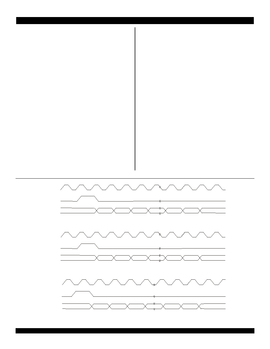
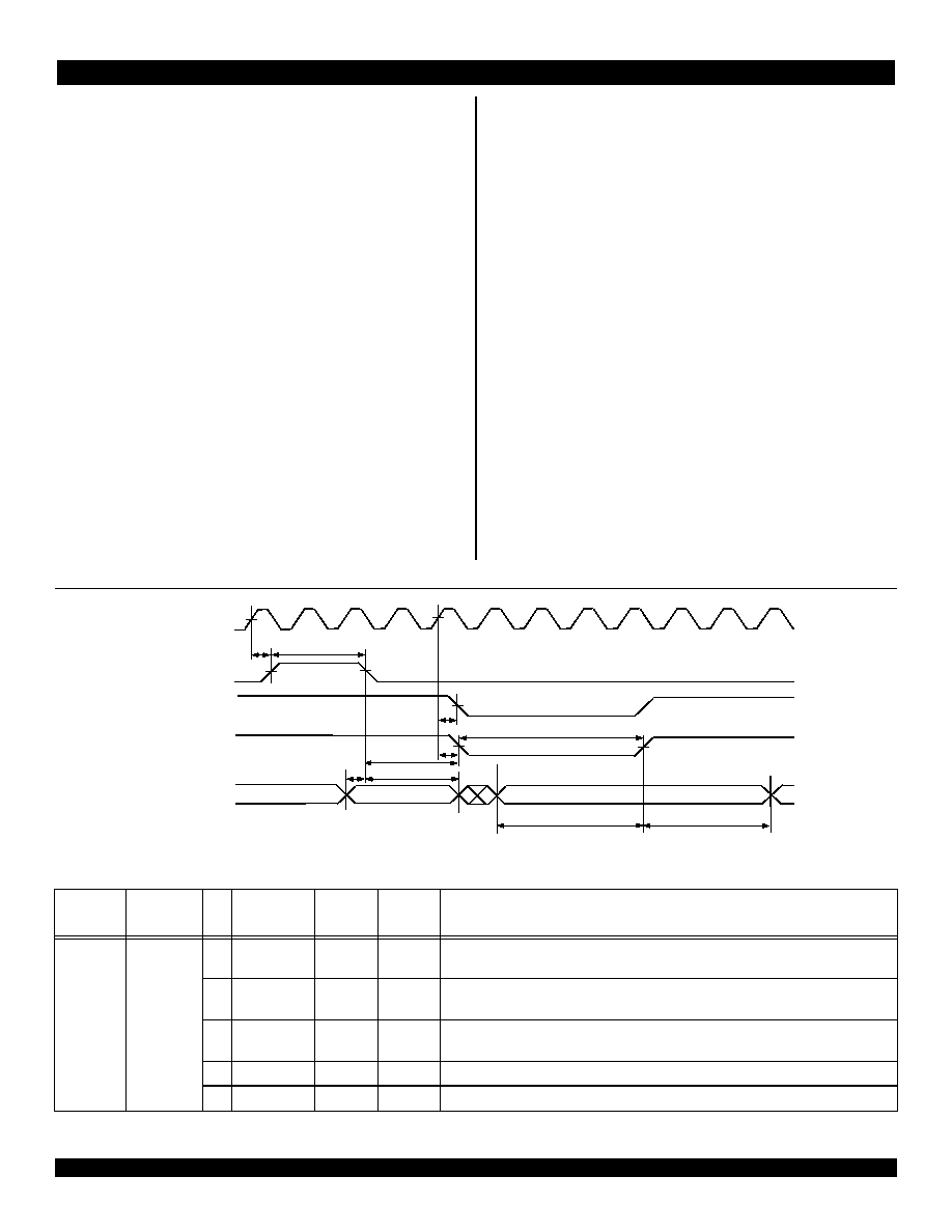
Figure 3 One Cell Transfer on Receive UTOPIA 1 Bus
Figure 4 Back-to-Back Cell Transfer without Tag Added
1
2
RCLK
(output)
RCLAV
(input)
R E N B
(output)
5347drw05
RSOC
(input)
RxDATA[7:0]
(input)
52
51
50
49
48
47
0
0
1
50
49
48
47
48
RCLK
(output)
RCLAV
(input)
R E NB
(output)
5347drw06
RSOC
(input)
RxDATA[7:0]
(input)
51
49
50
51
52
10 of 46
March 26, 2001
IDT77V012
Figure 5 One Cell Transfer on Transmit UTOPIA 1 Bus
Figure 6 Back-to-Back Cell Transfer without Tag Added
5HJLVWHU
1DPH
5HJLVWHU
$GGUHVV
%LW
%LW
1DPH
9DOXH
5DQJH
'HIDXOW
9DOXH
'HVFULSWLRQ
Configuration 2
8002
6
RxData Cell
Filter
0 - 1
0
Allow cells to be dropped on the receive UTOPIA interface. In-Stream
TM
cells are not affected by the condition of this bit, if they are being filtered on
the receive UTOPIA interface. "0" pass cells received on the receive UTO-
PIA interface, "1" filter and drop data cells on the receive UTOPIA interface.
Table 2 UTOPIA Receive Register Table
5HJLVWHU
1DPH
5HJLVWHU
$GGUHVV
%LW
%LW
1DPH
9DOXH
5DQJH
'HIDXOW
9DOXH
'HVFULSWLRQ
Configuration 2
8002
5
Drop Cell
0 - 1
0
Selects action if PHY transmit FIFO is full: "0" stall pipeline,
"1" drop cells.
Table 3 UTOPIA Transmit Register Table
5HJLVWHU
1DPH
5HJLVWHU
$GGUHVV
%LW
%LW
1DPH
9DOXH
5DQJH
'HIDXOW
9DOXH
'HVFULSWLRQ
Rx TAG and
Mode Select
8006
4
DPI Mode
0 - 1
Defined by
pin
Selects DRxCLK direction. "0" switch mode (output), "1" normal mode
(input).
Table 4 DPI Receive Register Table
1
TCLK
(output)
TCLAV
(input)
TEN B
(output)
5347drw07
TSOC
(output)
TxDATA[7:0]
(output)
51
50
49
48
47
0
46
1
46
TCLK
(output)
TCLAV
(input)
T E NB
(output)
5347drw08
TSOC
(output)
TxDATA[7:0]
(output)
49
48
47
0
49
52
50
51
11 of 46
March 26, 2001
IDT77V012
'3, ,QWHUIDFH
'3, ,QWHUIDFH
'3, ,QWHUIDFH
'3, ,QWHUIDFH
The Data Path Interface (DPI) is a synchronous bus interface
designed to transfer ATM cells between two devices. The 77V012 DPI
interface supports a 4-bit wide data bus (DPI-4), with separate transmit
and receive interfaces. All signals are sampled on the rising edge of
their respective clock.
'3,
'3,
'3,
'3, 5
5
5
5HFHL
HFHL
HFHL
HFHLYYYYH ,QWHUIDFH
H ,QWHUIDFH
H ,QWHUIDFH
H ,QWHUIDFH
The DPI Receive Interface is used to transfer cells from the 77V012
to the IDT SwitchStar or other DPI device. It has a 4-bit Output Data Bus
(DRxDATA[3:0]) and follows the standard DPI timing characteristics as
described in the DPI specification. Other signals associated with this
interface are DPI Receive Start of Frame (DRxFRM) and DPI Receive
Clock (DRxCLK).
DRxCLK operates at a frequency less than or equal to SCLK.
Depending on the DPI mode selected this clock will be either an input or
an output. In Normal Mode DRxCLK is an input to the 77V012. In Switch
Mode DRxCLK is a continuous clock generated by the 77V012. There is
no flow control in Switch mode, as it is assumed that the IDT SwitchStar
will be able to accept all incoming cells (non-blocking). Programming the
clock direction is done at reset.
DRxFRM is the start of frame marker. This signal is one DRxCLK
cycle long and is asserted high one DRxCLK cycle before the first nibble
of valid data.
'3
'3
'3
'3,,,, 7
7
7
7UUUUDQV
DQV
DQV
DQVP
P
P
PLW ,QWHU
LW ,QWHU
LW ,QWHU
LW ,QWHUIIIID
D
D
DF
F
F
FH
H
H
H
The DPI Transmit Interface is used to transfer cells from the IDT
SwitchStar or other DPI device to the 77V012. It has a 4-bit input data
bus (DTxDATA[3:0]) and follows the standard DPI timing characteristics
as described in the DPI specification. Other signals associated with this
interface are DPI Transmit Start of Frame (DTxFRM), and DPI Transmit
Clock (DTxCLK).
DTxCLK operates at a frequency less than or equal to SYSCLK.
DTxCLK can stop if the PHY device signals it cannot accept another cell
and the 77V012 has already started to stage the next cell to be trans-
ferred in its pipeline. When the PHY signals it can accept additional cells
DTxCLK will resume and the cell transfer will continue.
DTxFRM is the start of frame marker. This signal is one DTxCLK
cycle long and is asserted high one DTxCLK cycle before the first valid
nibble of data.
3
3
3
3UUUUR
R
R
RJU
JU
JU
JUD
D
D
DP
P
P
PPLQJ 3LQ &RQILJ
PLQJ 3LQ &RQILJ
PLQJ 3LQ &RQILJ
PLQJ 3LQ &RQILJXU
XU
XU
XUDEOH
DEOH
DEOH
DEOH
5
5
5
5HJ
HJ
HJ
HJLVWH
LVWH
LVWH
LVWHUUUUVVVV D
D
D
DWWWW 5
5
5
5HVHW
HVHW
HVHW
HVHW
A pull-up or pull-down resistor is connected to ADDR[11:0] signals to
select desired register values. The
SYSRST signal must be asserted for
at least one SYSCLK cycle to load the desired values. On the rising
edge of
SYSRST the 77V012 will begin loading the register values,
which takes an additional 16 SYSCLK cycles. During this 16 clock cycle
period all outputs will be tri-stated.
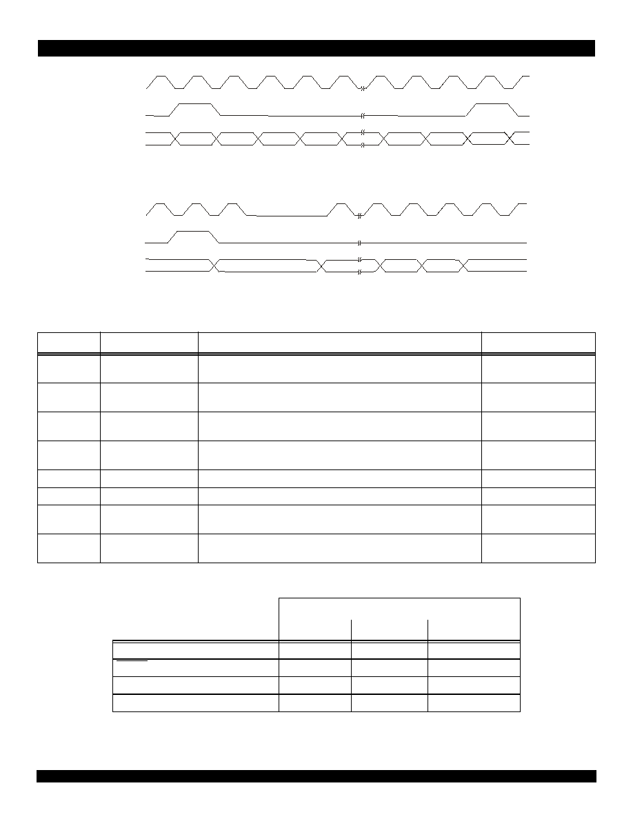
Figure 7 One Cell Transfer on Receive DPI Bus
Figure 8 Back-to-Back Cell Transfer on Receive DPI Bus
Figure 9 One Cell Transfer on Transmit DPI Bus
0
1
2
3
105
104
103
DRxCLK
(output)
DRxFRM
(output)
DRxDATA[3:0]
(output)
5347drw09
0
1
2
3
105
104
103
DRxCLK
(output)
DRxFRM
(output)
DRxDATA[3:0]
(output)
5347drw10
0
1
2
3
105
104
103
DTxCLK
(output)
DTxFRM
(input)
DTxDATA[3:0]
(input)
5347drw11
12 of 46
March 26, 2001
IDT77V012
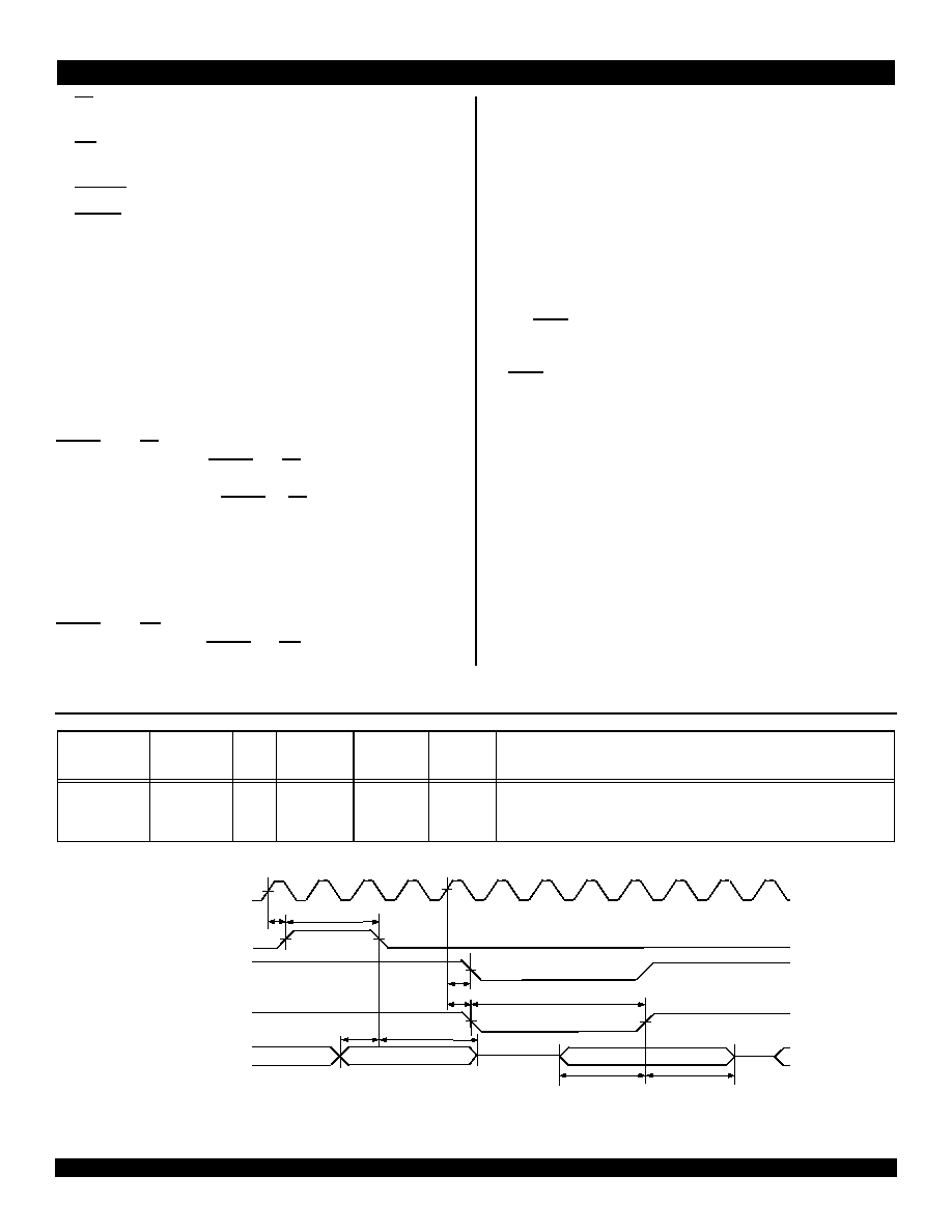
Figure 10 Back-to-Back Cell Transfers on Transmit DPI Bus
Figure 11 DTxCLK Stopping During Cell Transfer
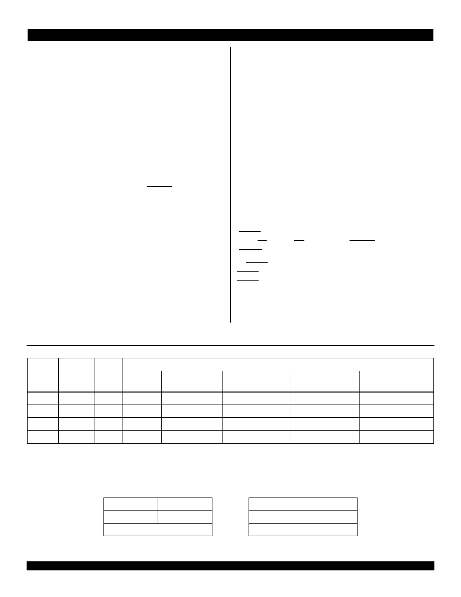
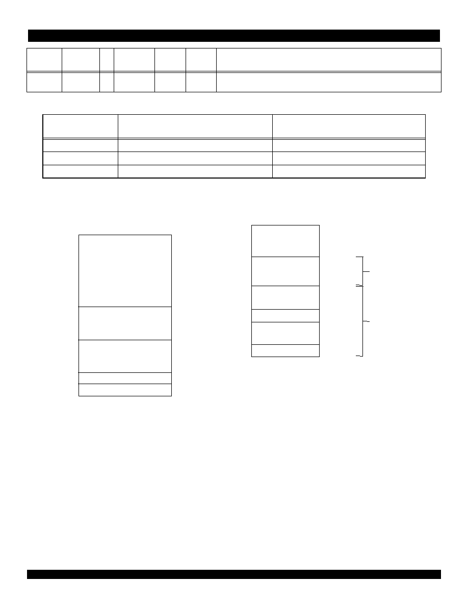
3LQ 1DPH
)XQFWLRQ # 5HVHW
2SWLRQV
5HJLVWHU
ADDR[2:0]
Tx TAG Size
Number of bytes to remove from the cell in the transmit direction. Valid values are
from zero to four bytes.
Tx TAG [2:0]
ADDR[3]
Tx TAG Location
"Location of the TAG in the transmit direction. "0" beginning of the cell, "1" end of
the cell."
Tx TAG [3]
ADDR[4]
Tx Add HEC
"Add a HEC placeholder to the cell. "0" do not add HEC placeholder, "1" add HEC
placeholder."
Tx TAG [4]
ADDR[7:5]
Rx TAG Size
Number of bytes to add to the cell in the receive direction. Valid values are from
zero to four bytes.
Rx TAG and Mode Select [2:0]
ADDR[8]
Rx Remove HEC
"Remove HEC byte from cell. "0" do not remove HEC byte, "1" remove HEC byte." Rx TAG and Mode Select [3]
ADDR[9]
DPI Mode
"Selects direction of DRxCLK. "0" switch mode (output), "1" normal mode (input)."
Rx TAG and Mode Select [4]
ADDR[10]
In-StreamTM Direction
"Interface to filter In-StreamTM programming cells. "0" filter on transmit DPI inter-
face, "1" filter on receive UTOPIA interface."
Rx TAG and Mode Select [5]
ADDR[11]
Init from EEPROM
"Write four bytes from EEPROM to In-StreamTM Cell Header registers. "0" do not
write four byte value, "1" write four byte value."
Rx TAG and Mode Select [6]
Table 5 Reset Configuration Pins
'HYLFH WR EH 5HVHW
9
3+< 'HYLFH
6HDUFK 7DEOH
Software Reset (In-Stream
TM
)
X
SYSRST (external pin)
X
X
PHY reset (register bit)
X
Search Table Reset (register bit)
X
Table 6 Reset Table
0
1
2
3
105
104
103
DTxCLK
(output)
DTxFRM
(input)
DTxDATA[3:0]
(input)
5347drw12
105
104
0
0
1
105
104
103
DTxCLK
(output)
DTxFRM
(input)
DTxDATA[3:0]
(input)
5347drw13
13 of 46
March 26, 2001
IDT77V012
5
5
5
5H
H
H
HVHW 2SWLRQV
VHW 2SWLRQV
VHW 2SWLRQV
VHW 2SWLRQV
Resetting the 77V012 can be accomplished with either the external
pins or In-StreamTM programming cells, while the PHY and Search
Tables are reset with In-StreamTM cells.
The System Reset (
SYSRST) pin will reset the 77V012 and the PHY
devices when asserted low. The 77V012 can also be reset with an In-
StreamTM cell carrying the Reset command (Message Type ID 0x3),
however, this command does not reset the PHY device. When using the
SYSRST pin the device will stay in reset for 16 SYSCLK cycles after the
rising edge of
SYSRST.
The PHY can be reset at any time by writing a one to the PHY Reset
bit of the Reset register. Writing a one will toggle the external
PHYRST
pin low for 16 SYSCLK cycles, while the PHY is being reset. This bit will
return to zero once the reset command is completed. This method will
only reset the PHY device connected to the PHYRST pin.
The Search Table is reset by writing a one to the Search Table Reset
bit of the Reset register. Writing a one to this register bit will fill the
Search Table with Null pointers, which takes 1K to 12K SYSCLK cycles
depending on the size of the Search Table. This command only resets
the Search Table in the SRAM.
Cells can be dropped on the Rx UTOPIA interface by setting the
RxData Cell Filter bit of the Configuration 2 register. When this bit is set
to a one the 77V012 will drop all data cells and filter only In-StreamTM
cells, if In-StreamTM filtering is being done on the Rx UTOPIA interface.
A hardware reset will clear this bit, while a software reset will not. This
register bit must be written to disable the function after a software reset
has occurred. When enabled the receive cell counters are disabled,
which includes both the UTOPIA Rx Cell Counter registers and the Rx
Counters in the Result Node. The transmit section is not affected by this
bit.
%D
%D
%D
%DQ
Q
Q
QGZLGW
GZLGW
GZLGW
GZLGWK
K
K
K DQG &OR
DQG &OR
DQG &OR
DQG &ORF
F
F
FN 6S
N 6S
N 6S
N 6SH
H
H
HHGV
HGV
HGV
HGV
The 77V012 can run at a maximum SYSCLK speed of 66MHz. The
DPI clocks must run at 40MHz, or greater, to achieve 155.52Mbps data
rate with overhead. The Clock Speed vs. Bandwidth Table lists some of
the possible data rates and the clock frequencies required to achieve
them.
87
87
87
872
2
2
23,$
3,$
3,$
3,$ WR
WR
WR
WR '3, &
'3, &
'3, &
'3, &R
R
R
RQY
QY
QY
QYH
H
H
HUUUUVLRQ
VLRQ
VLRQ
VLRQ
Bit swapping must be performed to convert the 8-bit Tx and Rx of the
UTOPIA interface to the 4-bit Tx and Rx of the DPI interface. Cell
formatting is big endian, or upper nibble first. The UTOPIA to DPI
conversion table illustrates how the 77V012 performs cell formatting.
8WLOLW
8WLOLW
8WLOLW
8WLOLW\\\\ %XV ,QWHUIDFH
%XV ,QWHUIDFH
%XV ,QWHUIDFH
%XV ,QWHUIDFH
The Utility Bus interface is used to access the PHY registers. A one
to 32-byte read or write command is accomplished by using In-StreamTM
cells.
Signals associated with the Utility Bus Interface are Chip Select
(PHYCS), Address Latch Enable (ALE), Address/Data Bus (AD[7:0]),
Read (RD), Write (WR), PHY Reset (PHYRST) and PHY Interrupt
(PHYINT).
PHYCS is used to validate activity on the Utility Bus. When
PHYCS ="0" the Utility Bus is active with valid data transactions. When
PHYCS ="1" the Utility Bus is not selected.
ALE is an active high signal used to latch the address, on AD[7:0], in
the address phase of a Utility Bus read or write operation.
AD[7:0] is a byte wide multiplexed bi-directional bus used to read and
write data to the PHY.
SYSCLK
(MHz)
DTxCLK &
DRxCLK
(MHz)
TCLK &
RCLK
(MHz)
Bandwidth of UTOPIA Interface (cell rate in Mbps)
52 byte cell
(w/o HEC)
53 byte cell
(normal cell w/HEC)
54 byte cell (one byte if
TAG added w/HEC)
55 byte cell (two bytes
of TAG added w/HEC)
56 byte cell (four bytes of
TAG added w/o HEC)
40
40
20
157
157
144
144.3
140
44
44
22
172.7
172.7
158.4
158.7
154
50
50
25
196.2
196.3
180
180.3
175
66
66
33
259
259.1
237.6
238
231
Table 7 Clock Speed vs. Bandwidth Table
UTOPIADPI-4
bit 7
bit 0
bit 3
bit 0
GFC
VPI[7:4]
GFC
VPI[3:0]
VCI[15:12]
VPI[7:4]
VCI[11:4]
VPI[3:0]
Table 8 UTOPIA to DPI Conversion
14 of 46
March 26, 2001
IDT77V012
RD is an active low signal used as an enable to read data from an
addressed location on the AD[7:0] bus.
WR is an active low signal used as an enable to write data to an
addressed location on the AD[7:0] bus.
PHYRST is an active low PHY reset signal.
PHYINT is an active low interrupt signal. This signal is driven by the
PHY layer and indicates that an interrupt has occurred. The interrupt
must be cleared by the controlling CPU before another interrupt event
can be reported.
Registers associated with the Utility Bus interface are described in
the Utility Bus Register Table. The register address range is described in
the Address Map.
8WLOLW\ %XV
8WLOLW\ %XV
8WLOLW\ %XV
8WLOLW\ %XV 5
5
5
5HDG 2S
HDG 2S
HDG 2S
HDG 2SH
H
H
HUDWLRQ
UDWLRQ
UDWLRQ
UDWLRQ
A Utility bus read is initiated by an In-StreamTM programming cell.
Once the 77V012 interprets the cell as a read command it will drive
PHYCS, ALE, RD, and AD[7:0]. The PHY samples the address on the
falling edge of ALE. Once PHYCS and RD assert the bus tristates and
switches to an input for the PHY to place data on. The PHY drives the
bus until the rising edge of PHYCS or RD. One Utility Bus read can
include up to 32 bytes of data.
8WLOLW\ %XV ZULWH
8WLOLW\ %XV ZULWH
8WLOLW\ %XV ZULWH
8WLOLW\ %XV ZULWH 2SH
2SH
2SH
2SHUUUUD
D
D
DWLRQ
WLRQ
WLRQ
WLRQ
A Utility bus write is initiated by an In-StreamTM programming cell.
Once the 77V012 interprets the cell as a write command it will drive
PHYCS, ALE, WR, and AD[7:0]. The PHY samples the address on the
falling edge of ALE. Once PHYCS and WR assert the 77V012 will write
data to the PHY. One Utility Bus write can include up to 32 bytes of data.
((3
((3
((3
((352
52
52
520 ,
0 ,
0 ,
0 ,QWHU
QWHU
QWHU
QWHUIIIID
D
D
DF
F
F
FH
H
H
H
The EEPROM is an optional device that can be used for initialization
and Discovery/Identify cells. The data is broken up into five fields. Bytes
[3:0] contain a value that can be read at reset and placed in the In-
StreamTM Cell Header registers to be used for the In-StreamTM cell
header. Bytes [7:4] are not used at this time, while bytes [39:8] contain
32-bytes of data, which is read when a Discovery/Identify command is
encountered. Bytes 40 to 127 are reserved and bytes 128 to 255 are
user defined. The registers associated with the EEPROM are listed in
the EEPROM Register Table.
Signals associated with this interface are Clock (EECLK), Chip
Select (EECS), Data Out (EEDOUT), Data In (EEDIN), and ADDR[11].
EECLK is generated from SYSCLK and is an output of the 77V012.
EECS is an active low chip select signal used to validate a read or
write operation.
EEDOUT is a serial output data pin to the EEPROM.
EEDIN is a serial input data pin from the EEPROM.
At reset ADDR[11] selects whether or not to write the first four bytes
stored in the EEPROM to the In-StreamTM Cell Header registers. The
loading process starts on the rising edge of SYSCLK following the
completion of the reset cycle. The loading process takes approximately
2000 SYSCLK cycles to complete, at which time the value is loaded into
the registers.
The EEPROM can be controlled with the EEPROM register bits,
which include Mux Select (EEPROM Mux Sel), Clock Output (EEPROM
Clock Out), Chip Select (EEPROM Chip Select), Data Out (EEPROM
Out), and Data In (EEPROM In).
Figure 12 Utility Bus Read Operation
Register
Name
Register
Address
Bit
#
Bit
Name
Value
Range
Default
Value
Description
PHY Reset
800A
0
PHY Reset
0 - 1
0
When set high the PHYRST on the Utility Bus Interface will be asserted low
for 16 SYSCLK cycles. The register will reset to zero after the command is
executed.
Table 9 UTOPIA Receive Register Table
Address
ALE
PHYCS
Add/Data[7:0]
RD
Read Data from PHY
5347drw14
t
ALPW
t
AAL
t
ALA
t
ALR
t
RDPW
t
DRS
t
DRH
SYSCLK
t
PALE
t
PPHY
(I)
(O)
(I/O)
(O)
(O)
15 of 46
March 26, 2001
IDT77V012
EEPROM Mux Select indicates whether the EEPROM pins will be
connected to the In-StreamTM logic, or to the EEPROM registers. When
connected to the In-StreamTM logic 32-bytes of data are read from the
EEPROM if a Discovery/Identify command is filtered. Controlling the
EEPROM from the registers enables the user the flexibility of reading
and writing the EEPROM at any time. Programming is accomplished
with In-StreamTM cells regardless of the method used to access the
EEPROM.
EEPROM Clock Out is used to clock the EEPROM when it is being
controlled by the registers. This register must be written to twice to
execute one EEPROM clock cycle. You must write to the clock register
to perform a read or write command.
EEPROM Chip Select validates transactions on the EEPROM inter-
face when controlled by the EEPROM registers.
EEPROM Out is a 1-bit register used to output data to the EEPROM.
EEPROM In is a 1-bit register used to input data from the EEPROM.
65$0 ,QWHUIDFH
65$0 ,QWHUIDFH
65$0 ,QWHUIDFH
65$0 ,QWHUIDFH
The SRAM interface is used to connect the 77V012 to the synchro-
nous flow-through memory. The SRAM contains the Search Tree used
to translate the original incoming ATM cell header to the new ATM cell
header. The SRAM size is configurable and is dependent on the number
of connections desired, the complexity of the Search Tree, and whether
cell accounting is being used. Memory sizes can be from 64K x 32-bit to
256K x 32-bit. See the Memory Size Table for valid memory sizes.
Signals associated with this interface are Address [17:0]
(ADDR[17:0]), Data [31:0] (DATA[31:0]), SRAM Clock (SCLK), Address
Status (
ADSP), Global Write (GW), Chip Enable (CE) and Output
Enable (
OE).
During normal operation ADDR[17:0] is the address bus used to
access the SRAM. Only ADDR[15:0] are required if a 64K x 32-bit
SRAM is used. During reset ADDR[11:0] are input pins used to configure
TAG parameters, In-StreamTM cell direction, and initialization from
EEPROM.
DATA[31:0] is a 32-bit bi-directional data bus used to read and write
data to the SRAM.
SCLK is a synchronous clock output used by the SRAM for all timing
references. It is the same frequency as the UTOPIA interface clock.
ADSP is a synchronous output used to load the SRAM address
registers with a new address.
GW is a synchronous global read/write enable.
CE is an active low chip enable.
OE is an active low output enable.
The SRAM address range is described in the Address Map.
Figure 13 Utility Bus Write Operation
Register
Name
Register
Address
Bit
#
Register
Name
Value
Range
Default
Value
Description
Pin Control
8004
3
EEPROM Mux
Select
0 - 1
0
"Indicates if the EEPROM interface will be connected to the internal logic or the EEPROM
registers. "0" connected to internal logic, "1" connected to EEPROM registers."
4
EEPROM
Clock Out
0 - 1
0
"EEPROM clock when EEPROM interface is connected to the EEPROM registers. "0"
clock low, "1" clock high."
5
EEPROM Chip
Select
0 - 1
0
"EEPROM chip select when EEPROM interface is connected to the EEPROM registers.
"0" EEPROM interface is selected, "1" EEPROM interface is not selected."
6
EEPROM Out 0 - 1
0
EEPROM output bus when EEPROM interface is connected to the EEPROM registers.
7
EEPROM In
0 - 1
0
EEPROM input bus when EEPROM interface is connected to the EEPROM registers.
Table 10 EEPROM Register Table (Part 1 of 2)
Address
ALE
P H Y C S
Add/Data[7:0]
W R
Write Data to PHY
5347drw15
t
ALPW
t
AAL
t
ALA
SYSCLK
t
PALE
t
PPHY
t
ALW
t
DWH
t
DWS
(I)
(O)
(O)
(O)
(O)
t
WRPW
t
AW
16 of 46
March 26, 2001
IDT77V012
Rx TAG and
Mode Select
8006
6
Init from
EEPROM
0 - 1
0
"Four byte write from EEPROM to In-StreamTM Cell Header registers at reset. "0" do not
write four byte value, "1" write four byte value to registers."
Total Memory
Allocated
Best Case Connections Supported
(cell accounting enabled)
Worst Case Connections Supported
(cell accounting enabled)
64K x 32
13K
1
1.
Best case conditions are limited by the Result Node, which uses a memory block that is 64Kx32-bit in size.
2.5K
2
2.
This worst case condition is cased by all structures using the same 64Kx32-bit block of memory.
128K x 32
16K
1
5K
3
3.
Worst case conditions are determined by the number of Search Trees. This worst case condition uses one Search Tree, which resides in a 64Kx32-bit block of memory.
256K x 32
16K
1
5K
3
Table 11 Memory Size Table
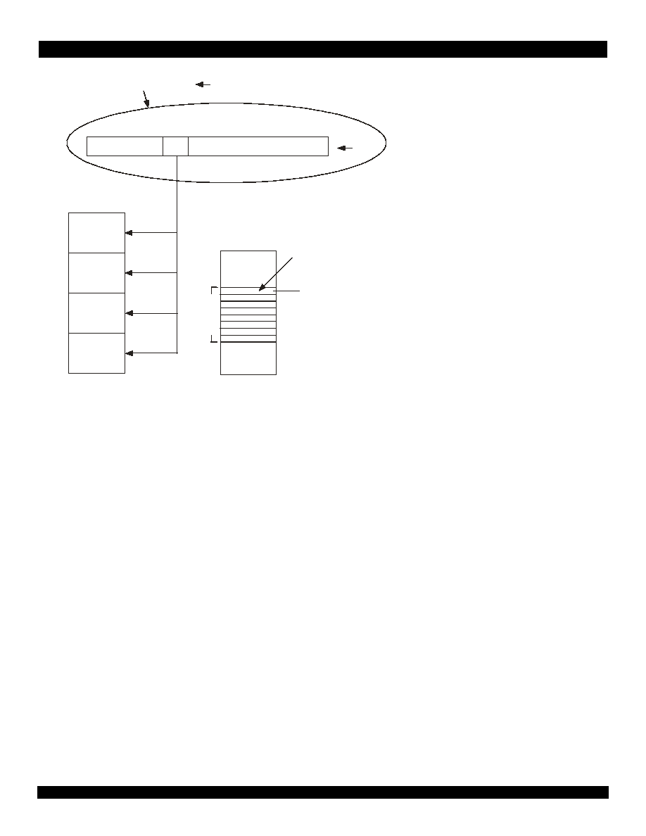
Figure 14 Address Map
Figure 15 EEPROM Memory Map
Register
Name
Register
Address
Bit
#
Register
Name
Value
Range
Default
Value
Description
Table 10 EEPROM Register Table (Part 2 of 2)
0
3
4
7
8
39
40
127
128
255
User Defined
Reserved
Discovery/Identify
cell data
Reserved
In-StreamTM cell header
5347drw16
Byte
PHY Registers
Reserved
77V012 Registers
Reserved
SRAM
(either 64K, 128K,
or 256K)
Reserved
0x000000
0x0000FF
0x000100
0x007FFF
0x008000
0x008025
0x008026
0x07FFFF
0x83FFFF
0x800000
0x840000
0xFFFFFF
5347drw17
Aligned on word boundary
(32-bits = 1 word)
Aligned on byte boundary
(8-bits = 1 byte)

17 of 46
March 26, 2001
IDT77V012
Number of Bits
Used in Search
Number of Bits Used
for Direct Lookup
Accesses to Locate
Search Table
Accesses Used to
Transverse SearchTree
Total Number of
Accesses Requited
24
8
1
8
9
28
12
1
8
9
28
8
1
10
11
32
12
1
10
11
Table 12 SRAM Memory Access Table
$
$
$
$70 +
70 +
70 +
70 +HDG
HDG
HDG
HDGH
H
H
HUUUU 7
7
7
7UUUUDQV
DQV
DQV
DQVOOOOD
D
D
DWLRQ
WLRQ
WLRQ
WLRQ
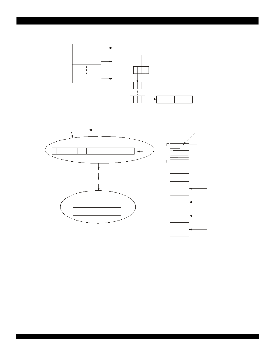
The search of a new header is the combination of a direct lookup
table and a search tree, which can be conducted on either 8, 12, 24, 28
or 32-bits of the cell header.
+HDGHU /RR
+HDGHU /RR
+HDGHU /RR
+HDGHU /RRN
N
N
NXS
XS
XS
XS
The first level of search is a direct lookup in the Search Table. The
result from this level of search will return the top node of a Search Tree,
with up to 4K unique Search Trees in the Search Table. The direct
lookup search is conducted on either the first 8 or 12-bits of the VPI field.
The Search GFC bit of the Configuration 1 register determines how
many bits to use for the direct lookup Search Table. When Search GFC
bit equals one the lookup is conducted using the first 12-bits of the
header. When the Search GFC bit is set to a zero an 8-bit lookup is
implemented, which uses the first 12-bits minus the 4-bit GFC field.
The number of bits being used for the direct lookup Search Table
determines the amount of memory required for the Search Table. The
Search Table is located in memory on 4K x 32-bit block boundaries.
When 12-bits are used for the search the table is 4K x 32-bits, when 8-
bits are being used the size of the Search Table will be 256 x 32-bits.
The search offset value, programmed through the Search Table Offset
[5:0] of the Table Offset register, is used as the base pointer address.
The direct lookup returns an address to a 32-bit memory location
[31:0], which contains a 18-bit pointer and a 1-bit indicator. Bits [17:0]
are the 18-bit pointer and bit [31] is the Tunneling Bit. The Tunneling bit
and the VPI Tunneling Enable bit of the Configuration 1 register indicate
what type of node the 18-bit pointer is pointing to, either a Search Table
Node or a Tunneling Node.
When the result is a Search Table Node, the search is continued by
using the next two bits of the header. The two bits are combined with the
Root Node, returned from the initial level of search, to traverse the next
level of the Search Tree. The result of the two bit search is a 16-bit
address that points to either a Non Terminal Node or a Leaf Node.
A Non Terminal Node is combined with the next two bits of the
header to form a pointer for the next level of search. The two bits are
combined with the Root Node of the previous level of search. The result
of this two bit search is either another Non Terminal Node or a Leaf
Node.
A Leaf Node is a 16-bit address returned from the last level of
search. The Leaf Node is combined with the Result Node Offset and
Result Bit to form a Result Node Pointer. The Result Node Pointer points
to a Result Node that contains either two 32-bit words or four 32-bit
words.
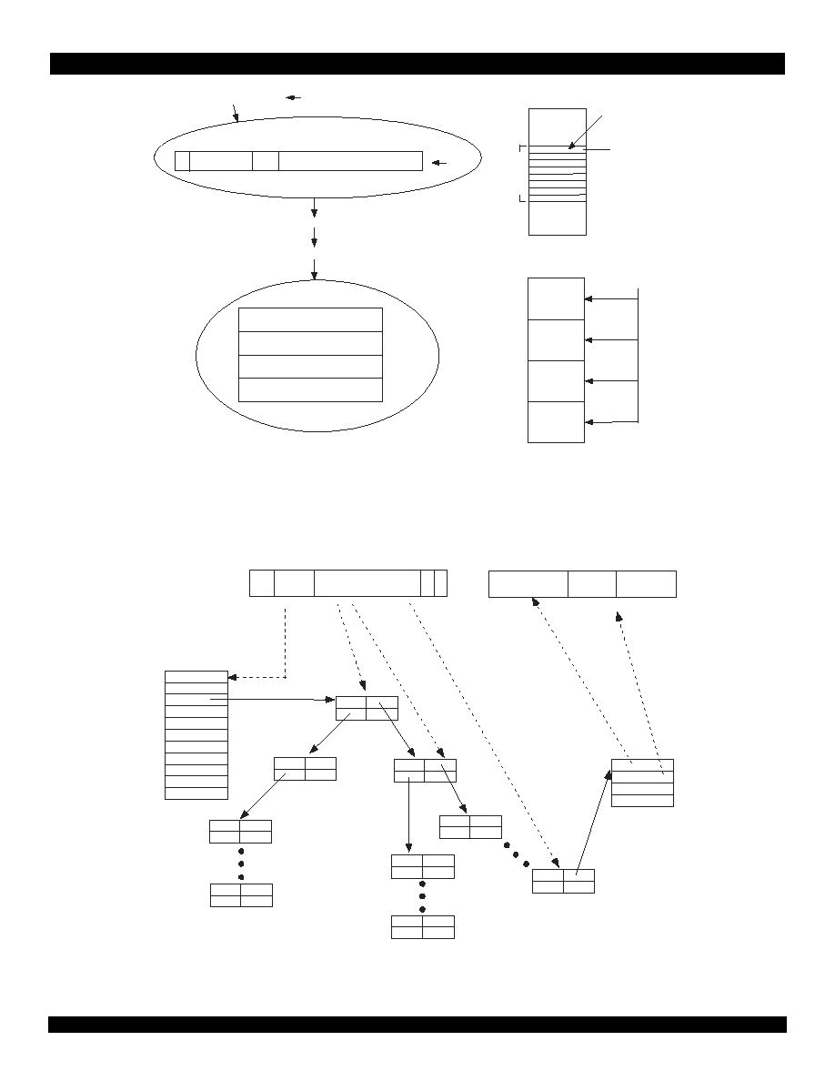
When the Tunneling bit of the Tunneling Node is equal to one and the
VPI Tunneling Enable bit of the Configuration 1 register is set to a one
the 18-bit pointer returned from the direct lookup points to a Result
Node. The Result Node contains either two or four 32-bit words. When
the Tunneling option is enabled the VCI value will not be overwritten.
The new header contains the new VPI value, the new GFC value if the
Overwrite GFC option is selected, and the new PT/CLP value if the
Overwrite PT/CLP option is selected.
The Result Node contains the TAG, new cell header and cell
accounting information, if enabled. The first 32-bit word of the Result
Node contains the TAG, the second 32-bit word contains the new cell
header, the third word is the Rx Cell Counter and the fourth word is the
Tx Cell Counter. The Rx and Tx Cell Counters are enabled by setting the
Cell Accounting On bit in the Configuration 1 register to a one.
All tables in the SRAM use programmable offset pointers. There are
generally two dedicated areas in the memory, one 4K block for the
search table and one 0-64K block for the Result Nodes. The remaining
memory is used for the Search Trees.
There are several registers associated with the SRAM memory and
the searching of a new header. A description for each register is given in
the Search Tree Register table.
6
6
6
65
5
5
5$
$
$
$0
0
0
0 0
0
0
0HPR
HPR
HPR
HPRUUUU\ $FF
\ $FF
\ $FF
\ $FFH
H
H
HVVHV
VVHV
VVHV
VVHV
The number of header bits and the type of search determines the
number of memory accesses required to complete the search. Refer to
the SRAM Memory Access Table for possible lookup combinations and
the number of accesses required.
The Result Node Tx and Rx cell counters may require additional read
and write cycles to the SRAM. When cell accounting is disabled the Tx
Counter does not require any additional read or write cycles, while the
Rx path requires two read cycles and no write cycles. When cell
accounting is enabled the Tx path requires one read and one write
cycle, while the Rx path requires three read cycles and one write cycle.
18 of 46
March 26, 2001
IDT77V012
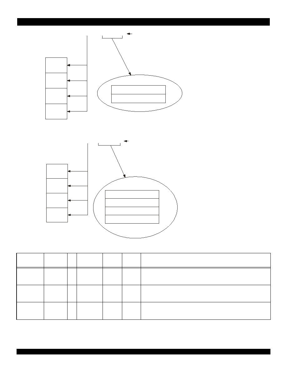
Figure 16 Lookup Search Table and Search Tree
Figure 17 Header Lookup with VPI Tunneling Enabled, Cell Accounting Disabled
0
1
2
4095
12-bit VPI Lookup Search Table
(one level of search)
0 1 2 3
0 1 2 3
0 1 2 3
TAG
New Header
16-bit VCI Search Tree
(up to ten levels of search)
5347drw18
64K
64K
64K
64K
256Kx32-bit SRAM
00
01
10
11
31
0
RNO
31:30
18:17 16:15
0
DC
TLN
4
K
o
r
2
5
6
b
l
o
c
k
o
f
m
e
m
o
r
y
SO
TN
64Kx32-bit Memory Block
2-bits
16-bits
Tunneling Node (TN) - 32-bit field returned from the
first level of search.
Tunneling Bit (TB) - 1-bit field indicating if the search
is a VPI tunneling search or a full header lookup.
5347drw19
{SO [5:0]; VPI [11:0]}
18-bit address used for first level of search
Tunneling Leaf Node (TLN) - 16-bit field returned from
the first level of search. This address points to a Result
Node.
TB
1-bit
Result Node Offset (RNO) - Offset for memory area used
to store the Result Nodes. This register value divides the
memory into 64Kx32-bit blocks.
Don't Care (DC) - A 2-bit don't care field.
RB = 0
RB = 1
31
0
TAG
New ATM Header
TN
{RNO [1:0]; TLN [15:1];RB [0]}
TB = 1
Search Offset (SO) - 6-bit offset pointer that points
to a 64Kx32-bit memory block and the starting
position of the Search Tree.
Result Bit (RB) - 1-bit field indicating what 32-bit
entry RNP is pointing to. RB = 0 points to the TAG
and RB=1 points to the new ATM header.
Search Table
19 of 46
March 26, 2001
IDT77V012
Figure 18 Header Lookup with VPI Tunneling Enabled, Cell Accounting Enabled
Figure 19 Header Lookup
64K
64K
64K
64K
256Kx32-bit SRAM
00
01
10
11
31
0
RNO
31:30
18:17 16:15
0
DC
TLN
4
K
o
r
2
5
6
b
l
o
c
k
o
f
m
e
m
o
r
y
SO
TN
64Kx32-bit Memory Block
2-bits
16-bits
5347drw20
{SO [5:0]; VPI [11:0]}
18-bit address used for first level of search
TB
1-bit
RB = 00
RB = 01
31
0
TAG
New ATM Header
TN
{RNO [1:0]; TLN [15:2];RB [1:0]}
TB = 1
Rx Counter
Tx Counter
RB = 10
RB = 11
Result Bit (RB) - 2-bit field indicating what 32-bit
entry the Result Node pointer is pointing to. RB =
00 points to the TAG, RB=01 points to the new ATM
header, RB=10 points to the Rx Counter and RB=11
points to the Tx Counter.
Search Table
GFC
VPI
VCI
PT
C
L
P
Input Header
{
{
{
{
{
{
{
31
0
4K Entries
(12-bit
look-up)
256
Entries (8-
bit look-
up)
31
0
31
0
31
0
31
0
31
0
31
0
31
0
31
0
TAG
New Header
Tx Counter
Rx Counter
}
Accounting
TAG
VPI
VCI
{
TAG + New Header
5347drw21
31
0
31
0
20 of 46
March 26, 2001
IDT77V012
Figure 20 Traversing the Search Tree for a 24-Bit Header
64K
64K
64K
64K
31
18:17 16:15
0
STO
RN
4
K
o
r
2
5
6
b
l
o
c
k
o
f
m
e
m
o
r
y
SO
STN (18-bits)
64Kx32-bit Memory Block
256Kx32-bit SRAM
00
01
10
11
2-bits
16-bits
31
0
Search Tree Offset (STO) - 2-bit field that points to one
of the 64Kx32-bit memory blocks. This 2-bit field is used
for all subsequent levels of search.
Search Offset (SO) - 6-bit offset pointer that points
to a 64Kx32-bit memory block and the starting position of
the Search Tree.
5347drw22
{SO [5:0]; VPI [11:0]}
18-bit address used for first level of search
STN
Root Node (RN) - 16-bit field combined with STO to create
STN.
Search Table Node (STN) - 18-bit field returned from the
first level of search. This address points to the top level
of a unique Search Tree.
Search Table
21 of 46
March 26, 2001
IDT77V012
Figure 21 Traversing the Search Tree (Continued)
31
16:15
0
SB1 = 1
SB1 = 0
16-bit address
16-bit address
Search Bit (SBx) - Indicates what entry
the 16-bit pointer is located in.
SB0 = 0
SB0 = 1
16-bit address
16-bit address
16-bit address
16-bit address
31
16:15
0
{STO[1:0]; NTN[15:1]; SB0[0]}
SB0 = 0 selects bits [15:0] of 32-bit entry
SB0 = 1 selects bits [31:16] of 32-bit entry
31
16:15
0
SB1 = 1
SB1 = 0
16-bit address
16-bit address
15
0
16-bit address
NTN
SB1 = 0 selects bits [15:0] of 32-bit entry
SB1 = 1 selects bits [31:16] of 32-bit entry
5347drw23
15
0
16-bit address
NTN
{STO[1:0]; STP[15:1]; SB0[0]}
Get next two bits of VCI = [SB0,SB1] and overwrite LSB (bit 0) of RN with SB0
SB0 = 0 selects the first 32-bit entry
SB0 = 1 selects the second 32-bit entry
SB1 = 0 selects bits [15:0] of 32-bit entry
SB1 = 1 selects bits [31:16] of 32-bit entry
Search Tree Pointer (STP) - 15-bit address returned
from the previous level of search. This is the 16-bit
returned address minus the LSB, which was overwritten
with SBx.
Non Terminal Node (NTN) - 16-bit field returned from
search. This 16-bit field is combined with STO and SBx
to form address for next level of search.
SB0 = 0
SB0 = 1
16-bit address
16-bit address
16-bit address
16-bit address
31
16:15
0
Get next two bits of VCI = [SB0,SB1] and overwrite LSB (bit 0) of NTN with SB0
A 16-bit Leaf Node (LN) is returned on the last level of search.
The Leaf Node points to a Result Node (RN).
Leaf Node (LN) - 16-bit field returned on the last level
of search. This field is combined with STO and RB to
form an 18-bit address that points to either the TAG,
New ATM Header, Tx Counter or Rx Counter.
Subsequent levels of search
15
0
16-bit address
LN
22 of 46
March 26, 2001
IDT77V012
Figure 22 Result Node without Cell Accounting
Figure 23 Result Node with Cell Accounting
Register
Name
Register
Address
Bit
#
Register
Name
Value
Range
Default
Value
Description
Configuration 1
8001
0
VPI Tunneling
Enable
0 - 1
0
"Enable VPI Tunneling. "0" header translation is done on the full header either 24,
28 or 32-bits, "1" header translation can be done with VPI Tunneling or full header
either 8, 12, 24, 28, or 32-bits."
1
Translation
Enable
0 - 1
0
"SRAM present, start search engine. "0" there is no SRAM attached, do not start
search engine, "1" SRAM is available and configured correctly for operation, start
search engine."
3
Cell Account-
ing On
0 - 1
0
"Indicates if cell counting on a per VC basis is enabled. Cell counting is done in both
the Tx and Rx directions. "0" Cell Counting is disabled (result node is two 32-bit
words), "1" Cell Counting is enabled (result node is four 32-bit words)."
Table 13 Search Tree Register Table (Part 1 of 3)
64K
64K
64K
64K
256Kx32-bit SRAM
00
01
10
11
31
0
Result Node Pointer
Result Bit (RB) - 1-bit field indicating what 32-bit
entry RNP is pointing to. RB = 0 points to the TAG
and RB=1 points to the new ATM header.
Result Node Pointer (RNP) - 18-bit pointer to a
result node.
5347drw24
RB = 0
RB = 1
31
0
TAG
New ATM Header
{RNO[1:0]; LN[15:1]; RB[0]}
Result Node Offset (RNO) - Offset for memory area
used to store the Result Nodes. This value divides
the memory into 64Kx32-bit blocks.
6 4 K
6 4 K
6 4 K
6 4 K
2 5 6 K x 3 2 -b it S R A M
0 0
0 1
1 0
1 1
3 1
0
R es u lt N o d e P oin te r
R esu lt B it (R B ) - 2 -b it f ie ld in d ic a tin g w h a t 3 2 -b it
e n try th e R e s u lt N o d e p o in te r is p o in tin g to . R B =
0 0 p o in ts to th e T A G , R B = 0 1 p o in ts to th e n e w A T M
h e a d e r, R B = 1 0 p o in ts to th e R x C o u n te r a n d R B = 1 1
p o in ts to th e T x C o u n te r .
R esu lt N od e O ffs et (R N O ) - O ffs e t fo r m e m o ry a re a
u s e d to sto re th e R e s u lt N o d e s . T h is v a lu e d iv id e s
th e m e m o ry in to 6 4 K x 3 2 -b it b lo c k s.
R B = 0 0
R B = 0 1
3 1
0
T A G
N e w A T M H e a d e r
R B = 1 0
R B = 1 1
R x C o u n te r
T x C o u n te r
{R N O [1 :0 ]; L N [1 5 :2 ]; R B [1 :0 ]}
R esu lt N od e P o inter (R N P ) - 1 8 - b it p o in te r to a
re s u lt n o d e .
5347drw25

23 of 46
March 26, 2001
IDT77V012
4
Null Counting
On
0 - 1
0
"Enable Null Cell Counters. "0" Null Cell Counters are disabled, "1" Null Cell
Counters are enabled."
5
Search GFC
0 - 1
0
"Indicates if the GFC field will be included in the search. "0" do not include GFC field
in search (Search Table is 256 x 32-bits), "1" include GFC field in search (Search
Table is 4K x 32-bits)."
6
Search PT/CLP 0 - 1
0
"Indicates whether PT/CLP fields will be included in search. "0" do not include PT/
CLP fields in search (eight levels in Search Tree), "1" include PT/CLP fields in
search (ten levels in Search Tree)."
7
Pass All Cells
0 - 1
0
"Pass or drop Null cells. "0" drop cell when search leads to a null pointer, "1" pass all
cell even if they lead to a null pointer."
Configuration 2
8002
0
Insert New
Header
0 - 1
0
"Insert New Header. "0" do not replace existing header with new header from
search, "1" replace existing header with new header found in search."
1
Overwrite GFC 0 - 1
0
"Overwrite the GFC field with the new header value. "0" do not overwrite GFC field
with new value, "1" overwrite GFC field with new value found in search."
2
Overwrite PT/
CLP
0 - 1
0
"Overwrite the PT/CLP fields in the new cell header. "0" do not overwrite the PT/CLP
field of the original header with the PT/CLP value found in the search, "1" overwrite
the PT/CLP field of the new header with the PT/CLP value found in the search."
Table Offset
8003
5:0
Search Table
Offset
0x00 -
0x3F
0x00
Offset pointer for Search Table. Divides memory into 4K blocks.
7:6
Result Node
offset
0x0 - 0x3
0x0
Result node offset pointer. Divides memory into 64K blocks.
Reset
800A
1
Search Table
Reset
0 - 1
0
"Writes Null pointers into Search Table. "0" do not write Null pointers into Search
Table, "1" write Null pointers into Search Table (will reset back to zero once the
operation is completed in approx. 1K to 12K SYSCLK cycles depending on the size
of the Search Table). This value is obtained from the Null Pointer Address registers."
Null Pointer
Address Byte 2
800B
1:0
Null Pointer
[17:16]
0x0 - 0x3
0x3
Null pointer search tree address and value written in search tree.
Null Pointer
Address Byte 1
800C
[7:0] Null Pointer
[15:8]
0x00 -
0xFF
0xFF
Null pointer search tree address and value written in search tree.
Null Pointer
Address Byte 0
800D
[7:0] Null Pointer
[7:0]
0x00 -
0xFF
0xFF
Null pointer search tree address and value written in search tree.
Rx Null Pointer
Header Byte 3
8016
[7:0] Rx Null Pointer
Header [31:24]
0x00 -
0xFF
NA
Header filtered on receive DPI interface.
Rx Null Pointer
Header Byte 2
8017
[7:0] Rx Null Pointer
Header [23:16]
0x00 -
0xFF
NA
Header filtered on receive DPI interface.
Rx Null Pointer
Header Byte 1
8018
[7:0] Rx Null Pointer
Header [15:8]
0x00 -
0xFF
NA
Header filtered on receive DPI interface.
Rx Null Pointer
Header Byte 0
8019
[7:0] Rx Null Pointer
Header [7:0]
0x00 -
0xFF
NA
Header filtered on receive DPI interface.
Tx Null Pointer
Header Byte 3
801A
[7:0] Tx Null Pointer
Header [31:24]
0x00 -
0xFF
NA
Header filtered on transmit DPI interface.
Tx Null Pointer
Header Byte 2
801B
[7:0] Tx Null Pointer
Header [23:16]
0x00 -
0xFF
NA
Header filtered on transmit DPI interface.
Tx Null Pointer
Header Byte 1
801C
[7:0] Tx Null Pointer
Header [15:8]
0x00 -
0xFF
NA
Header filtered on transmit DPI interface.
Tx Null Pointer
Header Byte 0
801D
[7:0] Tx Null Pointer
Header [7:0]
0x00 -
0xFF
NA
Header filtered on transmit DPI interface.
Register
Name
Register
Address
Bit
#
Register
Name
Value
Range
Default
Value
Description
Table 13 Search Tree Register Table (Part 2 of 3)

24 of 46
March 26, 2001
IDT77V012
UTOPIA Rx Cell
Counter Byte 3
801E
[7:0] Rx Cell
Counter [31:24]
0x00 -
0xFF
0x00
Counter for cells received on receive UTOPIA bus.
UTOPIA Rx Cell
Counter Byte 2
801F
[7:0] Rx Cell
Counter [23:16]
0x00 -
0xFF
0x00
Counter for cells received on receive UTOPIA bus.
UTOPIA Rx Cell
Counter Byte 1
8020
[7:0] Rx Cell
Counter [15:8]
0x00 -
0xFF
0x00
Counter for cells received on receive UTOPIA bus.
UTOPIA Rx Cell
Counter Byte 0
8021
[7:0] Rx Cell
Counter [7:0]
0x00 -
0xFF
0x00
Counter for cells received on receive UTOPIA bus.
UTOPIA Tx Cell
Counter Byte 3
8022
[7:0] Tx Cell Counter
[31:24]
0x00 -
0xFF
0x00
Counter for cells transmitted on transmit UTOPIA bus.
UTOPIA Tx Cell
Counter Byte 2
8023
[7:0] Tx Cell Counter
[23:16]
0x00 -
0xFF
0x00
Counter for cells transmitted on transmit UTOPIA bus.
UTOPIA Tx Cell
Counter Byte 1
8024
[7:0] Tx Cell Counter
[15:8]
0x00 -
0xFF
0x00
Counter for cells transmitted on transmit UTOPIA bus.
UTOPIA Tx Cell
Counter Byte 0
8025
[7:0] Tx Cell Counter
[7:0]
0x00 -
0xFF
0x00
Counter for cells transmitted on transmit UTOPIA bus.
Register
Name
Register
Address
Bit
# Bit Name
Value
Range
Default
Value
Description
Notification
Mask
8007
0
PHY Interrupt
Mask
0 - 1
0
"Mask Interrupt notification. "0" no Event Notification cell will be generated when a
PHY interrupt occurs, "1" generate Event Notification cell when a PHY interrupt
occurs."
1
Rx Null Mask
0 - 1
0
"Mask Interrupt notification. "0" no Event Notification cell will be generated when Rx
Null pointer is encountered, "1" generate Event Notification cell when a Rx Null
pointer is encountered."
2
Tx Null Mask
0 - 1
0
"Mask Interrupt notification. "0" no Event Notification cell will be generated when Tx
Null pointer is encountered, "1" generate Event Notification cell when a Tx Null
pointer is encountered."
Status
8008
0
Interrupt Status 0 - 1
0
"Indicates that a PHY interrupt occurred. "0" no PHY interrupts detected, "1" PHY
interrupt has been detected on the PHYINT pin."
Rx Null Pointer
Status
0 - 1
0
"Indicates that a Rx Null pointer was encountered. "0" no Rx Null pointer has been
detected, "1" Rx Null pointer has been detected."
2
Tx Null Pointer
Status
0 - 1
0
"Indicates that a Tx Null pointer was encountered. "0" no Tx Null pointer has been
detected, "1" Tx Null pointer has been detected."
Timeout Status 8009
0
PHY Interrupt
Timer
0 - 1
0
"Indicates that a PHY interrupt occurred more than 25ms ago, and the Status regis-
ter has not been serviced. This bit is cleared by writing to the status register. "0" no
PHY interrupt detected, "1" PHY interrupt occurred more than 25ms ago and the
Status register has not been serviced."
1
Rx Null Pointer
Counter
0 - 1
0
"Indicates that a Rx Null pointer was encountered more than 25ms ago, and the Sta-
tus register has not been serviced. This bit is cleared by writing to the Status regis-
ter. "0" no Rx Null pointers detected, "1" Rx Null pointer encountered more than
25ms ago and the Status register has not been serviced."
2
Tx Null Pointer
Timer
0 - 1
0
"Indicates that a Tx Null pointer was encountered more than 25ms ago, and the Sta-
tus register has not been serviced. This bit is cleared by writing to the Status regis-
ter. "0" no Tx Null pointers detected, "1" Tx Null pointer encountered more than
25ms ago and the Status register has not been serviced."
Table 14 Interrupt Register Table
Register
Name
Register
Address
Bit
#
Register
Name
Value
Range
Default
Value
Description
Table 13 Search Tree Register Table (Part 3 of 3)

25 of 46
March 26, 2001
IDT77V012
1XOO
1XOO
1XOO
1XOO 3
3
3
3RLQWH
RLQWH
RLQWH
RLQWHUUUUVVVV
A Null pointer is a unique selectable value that indicates the pointer
is not valid and the search should be terminated. The Null pointer points
to a Result Node that contains the Tx and Rx Null Cell Counters. The Tx
and Rx Null Cell Counters are enabled by setting the Null Counting On
bit of the Configuration 1 register. The Null cell counters can be enabled
without enabling the Tx and Rx Cell Counters.
When a Null cell is encountered the cell is either dropped or passed,
depending on bit 7 of the Configuration 1 register. When the drop option
is enabled the search is cancelled and the header of the violating cell is
placed in either the Tx or Rx Null Pointer Header registers and the
appropriate Null counter is incremented, if enabled. An Event Notifica-
tion cell will be generated if the appropriate mask bit is set in the Notifi-
cation Mask register. The appropriate Null Pointer Status bit of the
Status register will be updated regardless of the condition of the Notifica-
tion Mask register bits. See the Search Tree Register Table for a
description of the Tx and Rx Null Pointer registers.
,QWH
,QWH
,QWH
,QWHUUUUS
S
S
SUUUUHWL
HWL
HWL
HWLQ
Q
Q
QJ DQG &OHDULQJ ,
J DQG &OHDULQJ ,
J DQG &OHDULQJ ,
J DQG &OHDULQJ ,Q
Q
Q
QWH
WH
WH
WHUU
UU
UU
UUXSWV
XSWV
XSWV
XSWV
When an interrupt occurs the Status register will indicate were the
interrupt occurred.
The PHY Interrupt, Rx Null and Tx Null Mask bits of the Notification
Mask register determine if an Event Notification cell will be generated
when an interrupt is encountered. The 77V012 will not generate an
Event Notification cell when an interrupt occurs if the bits are set to the
default zero, and will generate a Event Notification cell if set to a one.
The Timeout Status register is a read only register that indicates an
interrupt occurred more than 25ms ago. It is used to verify that the inter-
rupts are being serviced by the CPU. Once the interrupt is detected the
77V012 will monitor the appropriate bit of the Status register to deter-
mine if the interrupt is cleared. The 77V012 will generate a Event Notifi-
cation cell, appropriate mask bit must be set to a one, if the interrupt is
not cleared within 25ms of when the interrupt occurred and will set the
appropriate Timeout Status bit. It will generate additional Event Notifica-
tion cells on 12ms intervals, thereafter, until the interrupt is cleared. It is
the CPU's responsibility to clear the interrupt and/or notify higher layers
that an interrupt has been encountered. Interrupts are cleared by the
CPU writing to the Status register. Writing a one will clear the interrupt
and reset the register back to zero.
See Interrupt Register Table for description of interrupt registers.
&H
&H
&H
&HOOOOO $FFRXQWLQJ
O $FFRXQWLQJ
O $FFRXQWLQJ
O $FFRXQWLQJ
The Tx and Rx Cell Counters are enabled by writing a one to the Cell
Accounting On bit in the Configuration 1 register. When enabled (set to a
one) the Result Node becomes four entries deep, with the third entry
being the Rx Cell Counter and the fourth entry being the Tx Cell
Counter. Each counter is 32-bits and is implemented as a wrap around
counter. These are per VC counters.
A global cell count is stored in the UTOPIA Tx and Rx Cell Counter
registers. These counters are always enabled and will increment each
time a cell is transmitted or received over the UTOPIA interface. They
can be read at any time, and will roll over once the maximum cell count
is reached. The counters are reset by writing zeros to the register. See
Search Tree Register Table for register description.
The Result Node and Global Rx cell counters are disabled if the
RxData Cell Filter bit of the Configuration 2 register is set to a one. This
also includes the counting of In-StreamTM cells. The Tx cell counters are
not affected by this register bit.
Register
Name
Register
Address
Bit
#
Bit Name
Value
Range
Default
Value
Description
Configuration 2 8002
3
Rx Move PT/CLP
0 - 1
0
"Move the PT/CLP fields from the original header into the 4-byte TAG
area. "0" do not move the PT/CLP fields, "1" move PT/CLP fields."
Pin Control
8004
0
Override Pin Control 0 - 1
0
"Enables writing to pin configurable registers. "0" pin configurable registers
are read only, "1" pin configurable registers are read/write."
Rx TAG and
Mode Select
8006
[2:0] Rx Tag Size [2:0]
0x0 - 0x4 Defined by pin Number of bytes to add to the received cell.
3
Rx Remove HEC
0 - 1
Defined by pin "Remove HEC from cell. "0" do not remove HEC byte from cell, "1" remove
HEC byte from cell."
In-StreamTM
TAG Byte 3
8012
[7:0] In-StreamTM TAG
[31:24]
0x00 -
0xFF
0x00
TAG added to In-StreamTM programming cells.
In-StreamTM
TAG Byte 2
8013
[7:0] In-StreamTM TAG
[23:16]
0x00 -
0xFF
0x00
TAG added to In-StreamTM programming cells.
In-StreamTM
TAG Byte 1
8014
[7:0] In-StreamTM TAG
[15:8]
0x00 -
0xFF
0x01
TAG added to In-StreamTM programming cells.
Table 15 Interrupt Register Table
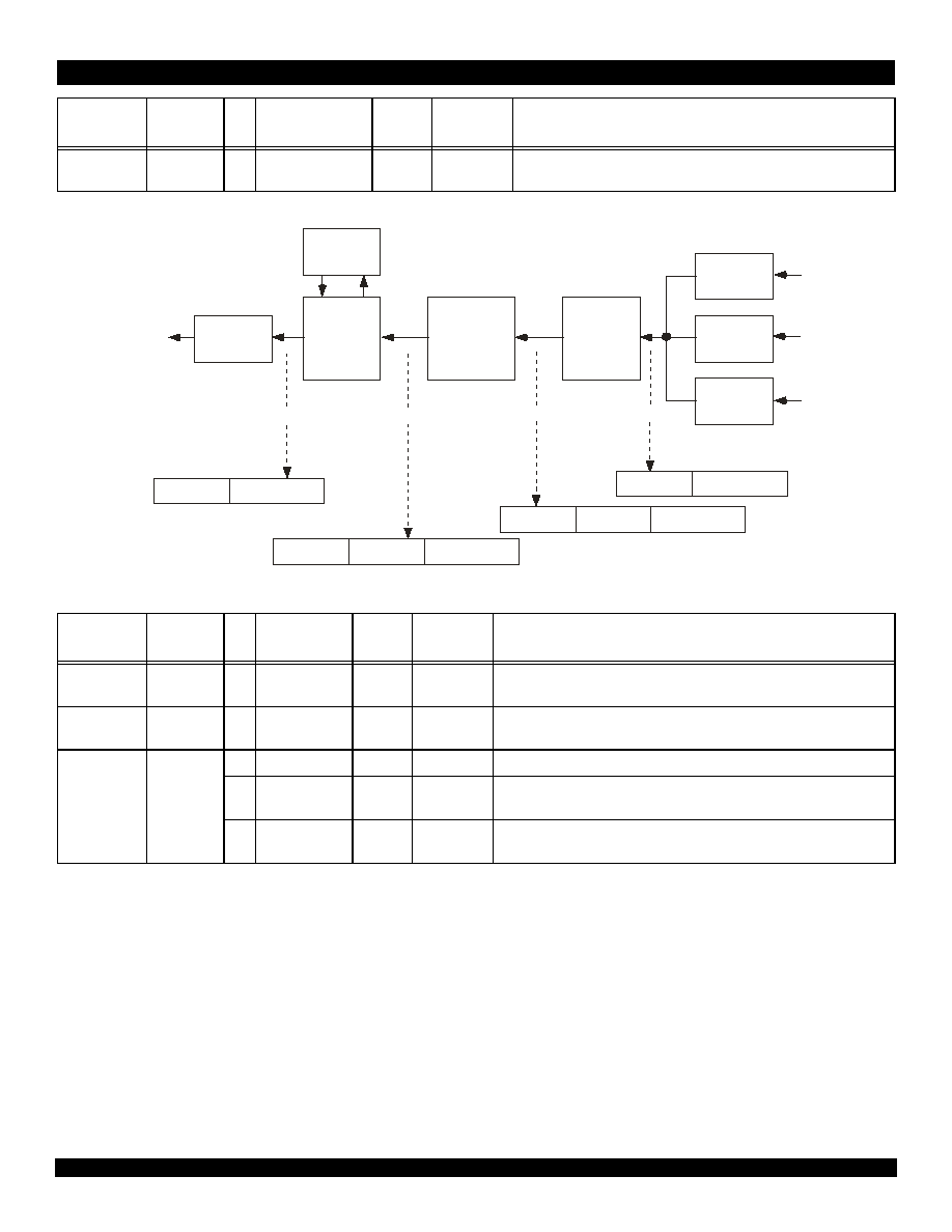
26 of 46
March 26, 2001
IDT77V012
Figure 24 Transmit Tag Routing Diagram
In-StreamTM
TAG Byte 0
8015
[7:0] In-StreamTM TAG
[7:0]
0x00 -
0xFF
0xF0
TAG added to In-StreamTM programming cells.
Register
Name
Register
Address
Bit
# Bit Name
Value
Range
Default
Value
Description
Configuration 2 8002
4
Tx Move PT/CLP 0 - 1
0
"Move the PT/CLP field from the 4-byte TAG area to the cell header. "0" do not
move PT/CLP fields, "1" move PT/CLP fields."
Pin Control
8004
0
Override Pin
Control
0 - 1
0
"Enables writing to pin configurable registers. "0" pin configurable registers are
read only, "1" pin configurable registers are read/write."
Tx TAG
8005
[2:0] Tx Tag Size [2:0] 0 - 4
Defined by pin Number of bytes to remove from the ATM cell.
3
Tx Tag Location
0 - 1
Defined by pin "TAG location in Tx direction. "0" TAG is located at beginning of cell, "1" TAG
is located at end of cell."
4
Tx Add HEC
0 - 1
Defined by pin "Add a HEC place holder in the Tx direction. "0" do not add a HEC place
holder, "1" add a HEC place holder."
Table 16 Interrupt Register Table
Register
Name
Register
Address
Bit
#
Bit Name
Value
Range
Default
Value
Description
Table 15 Interrupt Register Table
UTOPIA 1
Header
Payload
4-bit DPI
4-bit DPI
UTOPIA 2
Header
Payload
TAG
Header
Payload
TAG
Header
Payload
ATM PHY
OC-3
SRAM
IDT71V633
Header
Xlater
IDT77V012
SWITCHStAR
IDT77V400
&
IDT77V500
DPI to
UTOPIA 2
IDT77V011
ADSL PHY
ADSL PHY
ADSL PHY
5347drw26
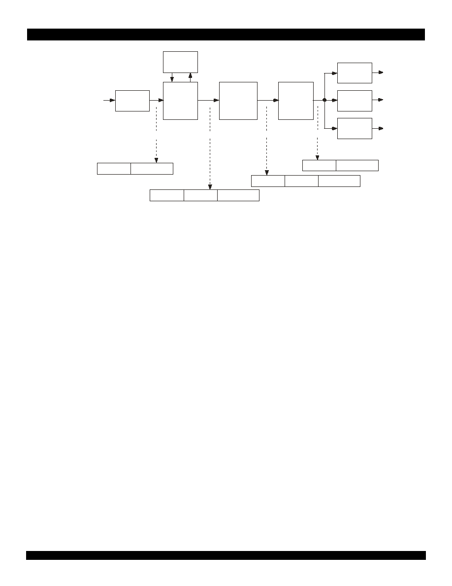
27 of 46
March 26, 2001
IDT77V012
Figure 25 Receive Tag Routing Diagram
UTOPIA 1
Header
Payload
4-bit DPI
4-bit DPI
UTOPIA 2
New Header
Payload
TAG
New Header
Payload
TAG
New Header
Payload
ATM PHY
OC-3
SRAM
IDT71V633
Header
Xlater
IDT77V012
SWITCHStAR
IDT77V400
&
IDT77V500
DPI to
UTOPIA 2
IDT77V011
ADSL PHY
ADSL PHY
ADSL PHY
5347drw27

28 of 46
March 26, 2001
IDT77V012
7
7
7
7D
D
D
DJ ,QWHUIDFH
J ,QWHUIDFH
J ,QWHUIDFH
J ,QWHUIDFH
A TAG can be added to the cell in the Rx direction and removed in
the Tx direction. It is added to the beginning of the cell and can be up to
four bytes long.
Programming the size of the TAG for both the Tx and Rx direction is
done with external pins and internal registers, with each direction being
individually programmed. The registers associated with the TAG are
listed in the Rx and Tx TAG Register Tables.
5
5
5
5H
H
H
HFHL
FHL
FHL
FHLYYYYH
H
H
H 7
7
7
7D
D
D
DJ
J
J
J
A TAG is added in the Rx direction by first configuring the external
pins and then configuring the internal registers. The external pins are
multiplexed with the SRAM address pins and are configured at reset.
ADDR[7:5] is a 3-bit field that sets the receive TAG size. This TAG
can be from zero to four bytes in size. The lower order bytes, in the
Result Node, are used when the TAG size is less than four bytes. There-
fore, a one byte TAG is appended to bits zero through seven of the
possible 32-bits in the TAG field. The value of ADDR[7:5] is stored in the
Rx TAG Size [2:0] bits of the Rx TAG and Mode Select register. The
header of the in coming cell will be appended to the TAG area when the
search engine is not enabled and four bytes of TAG are to be added.
When less than four bytes of TAG are added the most significant bytes
are appended.
ADDR[8] determines if the HEC byte should be removed or not.
Setting ADDR[8] low will leave the HEC byte intact, while setting
ADDR[8] high removes the HEC byte, thus reducing the number of
bytes in the cell by one. The value of ADDR[8] is stored in the Rx
Remove HEC bit of the Rx TAG and Mode Select register.
The In-StreamTM 1,2,3 and 4 registers indicate the value of the TAG
to be added to In-StreamTM programming cells. This value will only be
used for In-StreamTM cells. The default value is 0x000001FX, which can
be changed by writing to registers with In-StreamTM cells.
The Move PT/CLP bit of the Configuration 2 register will move the PT
and CLP fields of the new header value into the TAG area if set high and
will leave the original value intact if set low. Moving these fields, when
switching on the TAG area, enables a DPI device or SwitchStar to find
OAM cells, do low priority cell discards and EFCI processing. This option
is only valid if using all four bytes of TAG and switching is being done on
the TAG.
7
7
7
7UD
UD
UD
UDQVPLW
QVPLW
QVPLW
QVPLW 7
7
7
7D
D
D
DJ
J
J
J
A TAG is removed in the Tx direction by configuring the external pins,
which are multiplexed with the SRAM address pins ADDR[4:0].
ADDR[2:0] is a 3-bit field that sets the Tx TAG size. Valid TAG sizes
are from zero to four bytes. This value is stored in the Tx TAG Size bits
of the Tx TAG register.
ADDR[3] specifies if the TAG is located at the beginning or end of
the cell. When ADDR[3] ="0" the TAG is located at the beginning of the
cell, and when ADDR[3] ="1" the TAG is located at the end of the cell.
This value is stored in the Tx TAG Location bit of the Tx TAG register.
ADDR[4] specifies if a HEC placeholder is to be added to the cell.
When ADDR[4] = "0" a placeholder is not added, and if ADDR[4] = "1" a
placeholder is added to the cell. This value is stored in the Tx Add HEC
bit in the Tx TAG register.
,Q6W
,Q6W
,Q6W
,Q6WUUUUHDP
HDP
HDP
HDP
3
3
3
3UUUUR
R
R
RJU
JU
JU
JUDPPLQJ
DPPLQJ
DPPLQJ
DPPLQJ
In-StreamTM programming cells are used to carry commands to the
77V012 and for the CPU to receive information from the 77V012. Cells
are received on either the DTxDATA[3:0] bus or the RxDATA[7:0] bus,
depending on the condition of Instream Direction bit of the Rx TAG and
Mode Select register, which can be configured after reset.
All cells received on the selected data bus are filtered by the cell
interpreter to determine if they are In-StreamTM programming cells. In
order to be recognized, In-StreamTM programming cells have a unique
cell header. The default value is 0x000001FX, which can be changed by
writing to the In-StreamTM Cell Header 1, 2, 3 and 4 registers. All four
registers can be written to in one four byte write with an In-StreamTM
cell. The bytes are written MSB to LSB. The new cell header will be
used for returning a Reply Notification cell, following the write operation.
The 77V012 supports the following set of In-StreamTM functions,
Discover/Identify, Reset, Register Read, Register Write, Event Notifica-
tion and Reply Notification.
The Discover/Identify command is sent by the CPU to the 77V012,
and is used to either discover the 77V012 or to ensure that the 77V012
is still attached (heart beat).
The Reset command is sent from the CPU to the 77V012, which indi-
cates that the 77V012 must perform a hard reset and re-initialize itself to
its default state.
The Register Read command is used to read the value of one or
more registers. Up to 32-bytes can be read with one In-StreamTM cell.
The Register Write command is used to write a value to one or more
registers. Up to 32-bytes can be written with one In-StreamTM cell.
The Event Notification command is sent from the 77V012 to the CPU
and indicates that an event has happened that requires CPU interven-
tion.
The Reply Notification command is sent from the 77V012 to the CPU
in response to command cells sent by the CPU. The 77V012 will
generate a Reply Notification response to a Discover/Identify, Register
Read and Register Write command, but not for a Reset command. This
option is enabled by setting the Acknowledge Request bit in the
Message Type Field of the In-StreamTM command cell.
The In-StreamTM cell format is broken up into six sections, which
vary slightly depending on the type of command the cell caries.

29 of 46
March 26, 2001
IDT77V012
The first five bytes contain the cell header. The In-StreamTM
programming cell address is in the first 28-bits with the default value of
GFC =0x0, VPI =0x0, VCI =0x001F, PT/CLP =0xX, where X=don't care.
The remaining byte is the HEC.
Bytes six and seven of the cell contain the Transaction ID informa-
tion. This field is two bytes wide and is used to correlate messages
requiring a reply to a command. This allows more than one command to
be sent to a device without waiting for a Reply Notification cell, as the
field is copied from the Command cell to the Reply Notification cell. The
2-byte field is set to zero when an Event Notification cell is generated by
the 77V012, with the zero value being valid for this condition only. It is up
to the CPU to generate and manage values for it's In-StreamTM
commands and not re-use the value for some set amount of time.
Byte 8 contains the Message Type field, which indicates what type of
command the cell contains. Bit location eight is not used. Bit seven is the
Acknowledge Request bit, which indicates if an acknowledgement to the
Command cell is required or not. When a Reply Notification cell has to
be returned this bit is set to a one. When the Reply Notification cell is
returned the bit is reset to zero by the 77V012. This option is not valid
with the Reset command, which does not return a Reply Notification cell.
Bit six is the Acknowledge bit which indicates whether the cell is a Reply
Notification cell or a Command cell. This bit is set to a zero when the cell
is a Command cell, and is set to a one, by the 77V012, when the cell is a
Reply Notification cell. Bits one through five are the Message Type Indi-
cator. There are currently five commands for this field. The Discover/
Identify (value = 0x2) command, which will generate a Reply Notification
cell with 32 bytes of device specific data located in the Message Data
field. The Reset (value = 0x3) command performs a reset on the
77V012. There is no Reply Notification cell returned for this command.
The Read Registers (value = 0x5) command performs a read operation
to a set of consecutive registers. One to 31 bytes can be read with one
In-StreamTM cell starting at the specified base address when accessing
the 77V012 internal registers, while up to 32-bytes can be accessed with
one In-StreamTM cell when reading from the SRAM. The returned
register data is contained in the Message Data field. The Write Registers
(value = 0x6) command performs a write operation to a set of consecu-
tive registers. One to 31 bytes can be written with one In-StreamTM cell
starting at the specified base address when accessing the 77V012
internal registers, while up to 32-bytes can be accessed with one In-
StreamTM cell when writing to the SRAM.The data to be written is
contained in the Message Data field. The Event Notification (value =
0x8) command generates a Event Notification cell indicating that an
interrupt has been detected.
Bytes 9 through 15 are the Device ID field. There are two formats to
this field depending on the type of command the cell carries. When the
cell contains either the Register Read/Write, or Event Notification
command this field must contain a value of 0x01 in byte location 9 to be
valid. The remaining six bytes are not used and should contain zeros.
When the cell contains the Discovery/Identify command this field
contains data from the EEPROM, with data from EEPROM byte location
8 being written to the first byte position of this field.
Bytes 16 through 51 are the Message Data field. The layout of this
field is dependant on the Message Type field. A Read or Write command
will have a Message Data field divided into three sub fields. The first sub
field is one byte wide and indicates how many bytes of data are valid in
the data portion of the Message Data field. The second sub field is three
bytes wide and contains the base address for the Read or Write
command. The third sub field is the valid data and padding. Valid data is
written starting at the base address in accordance with the number of
valid bytes indicator (first sub field). The remaining space, if any, is
padded with zeros. A Discover/Identify command has a Message Data
field divided into two sub fields.The first sub field is the first 25-bytes of
the Message Data field, which contains up to 25 bytes read from the
EEPROM, starting at EEPROM byte location 15. The remaining bytes
are reserved. An Event Notification command will have a Message Data
field split into two sub fields. The first sub field is two bytes wide and
contains an event number, which is always 0x0100. The second sub
field contains one byte of data (byte 18) indicating what type of event
happened, which is described in the Event Notification Table. The
remaining bytes 19 to 51 are padding and contain zeros.
Bytes 52 and 53 contain the CRC-10 trailer, with the upper six bits of
byte 52 containing zeros. The CRC-10 is generated and used in the
same manner as in AAL3/4 cells.
1RW
1RW
1RW
1RWLLLLILF
ILF
ILF
ILFD
D
D
DWLRQ &HOOV
WLRQ &HOOV
WLRQ &HOOV
WLRQ &HOOV
The are two types of Notification cells, Event and Reply, that can be
generated by the 77V012.
The 77V012 will generate an Event Notification Cell under three
different conditions, if the appropriate mask bit(s) are set to a one. The
first condition occurs when an interrupt is detected on the external
PHYINT pin. The second condition is if a Rx Null Pointer is found in the
search, and the third is when a Tx Null Pointer is found in the search. It
is up to the CPU to clear the interrupt, or notify higher layers that an
interrupt has occurred. A second Event Notification cell will be gener-
ated if the interrupt is not cleared in 25ms. Additional Event Notification
cells will be generated every 12ms thereafter until the interrupt is
serviced. A new event will not be reported until the related interrupt
register bit has been cleared.
The 77V012 will generate a Reply Notification cell, if the Acknowl-
edge Request bit is set to a one. The Reply Notification cells enable the
CPU to keep status of its command cells.
0LV
0LV
0LV
0LVF
F
F
F )
)
)
)H
H
H
HD
D
D
DWX
WX
WX
WXUUUUHV
HV
HV
HV
The 77V012 offers two external control pins, CNTRL_A and
CNTRL_B, that can be connected to external devices for system design
engineer usage. Both of these signals are low after reset. There is also a
register bit associated with each signal, which is described in the Misc.
Register table.
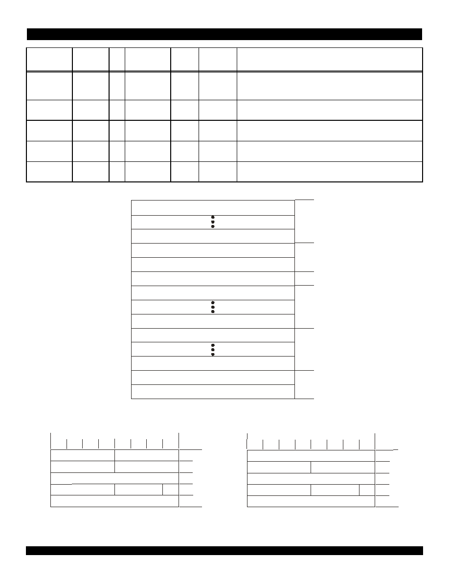
30 of 46
March 26, 2001
IDT77V012
Figure 26 General Format In-Stream
TM
Programming Cell
Figure 27 Valid Header Formats for In-Stream
TM
Programming Cell
5HJLVWHU
1DPH
5HJLVWHU
$GGUHVV
%LW
%LW 1DPH
9DOXH
5DQJH
'HIDXOW
9DOXH
'HVFULSWLRQ
Rx TAG and
Mode Select
8006
5
In-StreamTM
Direction
0 - 1
Defined by pin
ADDR[10]
"Indicates what interface the In-stream cells will be filtered on. "0" input on the
transmit DPI interface and output on the receive DPI interface, "1" input on
the receive UTOPIA interface and output on the transmit UTOPIA interface."
In-StreamTM Cell
Header Byte 0
800E
[7:0] In-StreamTM
Header [31:24]
0x00 -
0xFF
0x00
Cell header for In-StreamTM programming cells.
In-StreamTM Cell
Header Byte 1
800F
[7:0] In-StreamTM
Header [23:16]
0x00 -
0xFF
0x00
Cell header for In-StreamTM programming cells.
In-StreamTM Cell
Header Byte 2
8010
[7:0] In-StreamTM
Header [15:8]
0x00 -
0xFF
0x01
Cell header for In-StreamTM programming cells.
In-StreamTM Cell
Header Byte 3
8011
[7:0] In-StreamTM
Header [7:0]
0x00 -
0xFF
0xF0
Cell header for In-StreamTM programming cells.
Table 17 In-Stream
TM
Register Table
byte 1
byte 5
byte 6
byte 7
byte 8
byte 9
byte 15
byte 16
byte 53
byte 52
byte 51
ATM
Header
Message
Type
Transaction
ID
Device
ID
Message
Data
and/or
Padding
Trailer
5347drw28
UNI Cell Header (five byte field)
8
7
6
5
4
3
2
1
Bit
B
y
t
e
1
2
3
4
5
GFC
VPI
VPI
VCI
VCI
VCI
PT
CLP
HEC
5347drw29
NNI Cell Header (five byte field)
8
7
6
5
4
3
2
1
Bit
B
y
t
e
1
2
3
4
5
VPI
VPI
VCI
VCI
VCI
PT
CLP
HEC
5347drw30
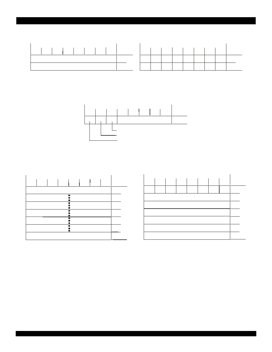
31 of 46
March 26, 2001
IDT77V012
Figure 28 Valid Transaction Field Formats for In-Stream
TM
Programming Cell
Figure 29 Valid Message Type Field Format for In-Stream
TM
Programming Cell
Figure 30 Valid Device ID Field Format for In-Stream
TM
Programming Cell
Command Cell Transaction ID (two byte field)
8
7
6
5
4
3
2
1
Bit
B
y
t
e
6
7
Notification Cell Transaction ID (two byte field)
8
7
6
5
4
3
2
1
Bit
B
y
t
e
6
7
5347drw31
0
0
0
0
0
0
0
0
0
0
0
0
0
0
0
0
Copied from Command Cell
Copied from Command Cell
8
7
6
5
4
3
2
1
Bit
B
y
t
e
8
Message Type ID
Acknowledge Bit
Acknowledge Request Bit
Not Used
Message Type (one byte field)
5347drw32
8
7
6
5
4
3
2
1
Bit
B
y
t
e
9
10
11
15
5347drw33a
Data from EEPROM
Discovery/Identify Command Cell
Device ID (seven byte field)
Data from EEPROM
12
13
14
Read/Write/Event Notification Command Cell
Device ID (seven byte field)
8
7
6
5
4
3
2
1
Bit
B
y
t
e
9
10
11
12
13
14
15
0
0
0
0
0
0
0
1
Not Used
Not Used
Not Used
Not Used
Not Used
Not Used
5347drw33
32 of 46
March 26, 2001
IDT77V012
Figure 31 Valid Message and/or Data Field Formats for In-Stream
TM
Programming Cell
Figure 32 Valid Trailer Field Format for In-Stream
TM
Programming Cell
1DPH
0HVVDJH 7\SH ,'
'HVFULSWLRQ
Discover/ Identify
2
This command will generate an Reply Notification cell containing 32 bytes of device specific data, which is stored
in bytes 8 through 40 of the EEPROM.
Reset
3
Performs a reset on 77V012 device. No Reply Notification cell is returned acknowledging that the reset command
has been completed.
Read Registers
5
Read from a consecutive number of registers.
Write Registers
6
Write to a consecutive number of registers.
Event Notification
8
An unsolicited Event Notification cell indicating an event has taken place. The event can be either a PHY interrupt,
a Rx Null pointer, or a Tx Null pointer.
Table 18 In-Stream
TM
Programming Message Type Indicator
Read/Write Command Cell
Message Data and/or Padding Field (36 byte field)
8
7
6
5
4
3
2
1
Bit
B
y
t
e
16
17
18
19
20
51
5347drw34
Number of valid bytes
Data and/or padding
Base address
Base address
Base address
Data and/or padding
Event Notification Cell
Message Data and/or Padding Field (36 byte field)
8
7
6
5
4
3
2
1
Bit
B
y
t
e
16
17
18
51
5347drw35
Data and/or padding
Data and/or padding
Event number
Event number
Discover/Identify Command Cell
Message Data and/or Paddind Field (36 byte field)
8
7
6
5
4
3
2
1
Bit
B
y
t
e
16
40
41
51
5347drw36
Data from EEPROM
Reserved
Reserved
Data from EEPROM
Trailer (two byte field)
8
7
6
5
4
3
2
1
Bit
B
y
t
e
52
53
5347drw37
0
0
0
0
0
0
CRC10
CRC10
33 of 46
March 26, 2001
IDT77V012
$
$
$
$& (OHFWULFD
& (OHFWULFD
& (OHFWULFD
& (OHFWULFDOOOO &KD
&KD
&KD
&KDUUUUDFWHULVWLFV
DFWHULVWLFV
DFWHULVWLFV
DFWHULVWLFV
(industrial: Vcc = 3.3V + 10%, TA = -40oC to 85oC)
%LW 1XPEHU
(YHQW
'HVFULSWLRQ
7:6
Not Used
5
Tx Null Pointer Error
A Null pointer has been detected in the transmit direction.
4
Tx Time Out
A Null pointer has been detected in the transmit direction, but the Status register has not been cleared.
3
Rx Null Pointer Error
A Null pointer has been detected in the receive direction.
2
Rx Time Out
A Null pointer has been detected in the receive direction, but the Status register has not been cleared.
1
PHY Interrupt Status
A PHY interrupt has been detected.
0
PHY Time Out
A PHY interrupt has been detected, but the Status register has not been cleared.
Table 19 Event Notification Table
5HJLVWHU
1DPH
5HJLVWHU
$GGUHVV
%LW
%LW 1DPH
9DOXH
5DQJH
'HIDXOW
9DOXH
'HVFULSWLRQ
Pin Control
8004
1
Control A
0 - 1
0
"Stores condition of Control A pin. "0" CTRL_A = "0", "1" CTRL_A = "1"."
2
Control B
0 - 1
0
"Stores condition of Control B pin. "0" CTRL_B = "0", "1" CTRL_B = "1"."
Table 20 Misc. Register Table
6\PERO
3DUDPHWHU
0LQ
0D[
8QLW
t
CYC
SYSCLK Cycle Time
15
--
ns
t
CH
SYSCLK High Time
6
--
ns
t
CL
SYSCLK Low Time
6
--
ns
t
UCYC
UTOPIA TCLK/RCLK Cycle Time
30
--
ns
t
UCH
UTOPIA TCLK/RCLK High Time
13
--
ns
t
UCL
UTOPIA TCLK/RCLK Low Time
13
--
ns
t
TOV
TxDATA, TENB, TSOC, TxPRTY, TxLED Output Valid from TCLK
1
20
ns
t
UTS
TCLAV to TCLK Setup Time
8
--
ns
t
UTH
TCLAV to TCLK Hold Time
1
--
ns
t
ROV
RENB, RxLED Output Valid from RCLK
1
20
ns
t
URS
RxDATA, RSOC, RCLAV to RCLK Setup Time
8
--
ns
t
URH
RxDATA, RSOC, RCLAV to RCLK Hold Time
1
--
ns
t
DCYC
DPI DTxCLK/DRxCLK Cycle Time
15
--
ns
t
DCH
DPI DTxCLK/DRxCLK High Time
6
--
ns
t
DCL
DPI DTxCLK/DRxCLK Low Time
6
--
ns
t
DTS
DTxFRM, DTxDATA to DTCLK Setup Time
6
--
ns
t
DTH
DTxFRM, DTxDATA to DTCLK Hold Time
2
--
ns
t
PDRD
DRxCLK to DRxDATA(0-3), DRxFRM Propagation Delay
--
8
ns
t
ALPW
ALE Pulse Width
30
--
ns
t
ALR
SYSCLK to RD Low Propagation Delay
--
20
ns
t
ALW
SYSCLK to WR Low Propagation Delay
--
20
ns
t
RDPW
RD Pulse Width
60
--
ns

34 of 46
March 26, 2001
IDT77V012
t
AAL
Address to ALE Falling Edge Setup Time
20
--
ns
t
ALA
Address to ALE Falling Edge Hold Time
10
--
ns
t
DRS
Data to rising edge of RD Setup Time
5
--
ns
t
DRH
Data to rising edge of RD Hold Time
1
--
ns
t
DWS
Data to rising edge of WR Setup Time
5
--
ns
t
DWH
Data to rising edge of WR Hold Time
1
--
ns
t
WRPW
WR Pulse Width
30
--
ns
t
PINTS
SYSCLK to PHYINT Setup Time
10
--
ns
t
PINTH
SYSCLK to PHYINT Hold Time
2
--
ns
t
AW
ALE falling edge to WR falling edge
30
--
ns
t
PALE
ALE to SYSCLK Propagation Delay
--
20
ns
t
PPHY
SYSCLK to PHYCS Propagation Delay
--
20
ns
t
PPHYR
SYSCLK to PHYRST Propagation Delay
--
20
ns
t
PRCLK
SYSCLK to RCLK Propagation Delay
--
15
ns
t
PTCLK
SYSCLK to TCLK Propagation Delay
--
13
ns
t
PDRxCLK
SYSCLK to DRxCLK Propagation Delay
--
10
ns
t
PDTxCLK
SYSCLK to DTxCLK Propagation Delay
--
10
ns
t
PCNTA
SYSCLK to CONT_A Propagation delay
--
20
ns
t
PCNTB
SYSCLK to CONT_B Propagation delay
--
20
ns
t
RSTW
SYSRST Pulse Width
100
--
ns
ts
CYC
SCLK Cycle Time
30
--
ns
ts
CH
SCLK High Time
13
--
ns
ts
CL
SCLK Low Time
13
--
ns
t
PADSP
SCLK to SRAM ADSP Propagation Delay
--
20
ns
t
POE
SCLK to SRAM OE Propagation Delay
--
9
ns
t
PADD
SCLK to SRAM Address Propagation Delay
--
20
ns
t
PDAT
SCLK to SRAM Dataout Propagation Delay
--
25
ns
t
SD
SCLK to SRAM Data In Setup Time
10
--
ns
t
HD
SCLK to SRAM Data In Hold Time
2
--
ns
t
ECYC
EECLK Cycle Time
1000
--
ns
t
PECLK
SYSCLK to EECLK, EECS, EEDOUT Propagation Delay
--
20
ns
t
SEDI
SYSCLK to EEDIN Setup Time
--
10
ns
t
HEDI
SYSCLK to EEDIN Hold Time
2
--
ns
6\PERO
3DUDPHWHU
0LQ
0D[
8QLW
35 of 46
March 26, 2001
IDT77V012
Figure 33 System Clock Timing Waveform
Figure 34 System Clock to UTOPIA Receive Clock Propagation Delay
Figure 35 System Clock to UTOPIA Transmit Clock Propagation Delay
Figure 36 System Clock to DPI Receive Clock Propagation Delay
Figure 37 System Clock to DPI Transmit Clock Propagation Delay
SYSCLK
5347drw38
t
CYC
t
CH
t
CL
SYSCLK
RCLK
tPRCLK
5347drw39
SYSCLK
TCLK
tPTCLK
5347drw40
SYSCLK
DRxCLK
tPDRxCLK
5347drw41
SYSCLK
DTxCLK
tPDTxCLK
5347drw42
36 of 46
March 26, 2001
IDT77V012
Figure 38 UTOPIA Transmit Timing Waveform
Figure 39 UTOPIA Receive Timing Waveform
Figure 40 DPI Transmit Timing Waveform
Figure 41 DPI Receive Timing Waveform
TCLK
5347drw43
TCLAV
TxDATA(0-7),
TENB
, TSOC,
TxLED, TxPRTY
t
TOV
t
UCH
t
UCL
t
UTS
t
UTH
t
UCYC
RCLK
5347drw44
RENB
, RxLED
RxDATA(0-7), RSOC, RCLAV
t
ROV
t
URS
t
URH
DTxCLK
5347drw45
DTxFRM, DTxDATA(0-3)
t
DTH
t
DCYC
t
DTS
t
DCH
t
DCL
DRxCLK
5347drw46
DRxFRM, DRxDATA(0-3)
t
PDRD
37 of 46
March 26, 2001
IDT77V012
Figure 42 System Clock to PHYRST Propagation Delay
Figure 43 System Clock to PHYINT Propagation Delay
Figure 44 SYSRST Timing Waveform
Figure 45 Timing Waveform for EEPROM Read and Write Cycles
SYSCLK
PH YR ST
5347drw47
tPPHYR
SYSCLK
PH YINT
5347drw48
tPINTH
tPINTS
SYSRST
5347drw49
tRSTW
SYSCLK
EECLK
EECS
EEDI
EEDO
5347drw50
t
PECLK
t
SEDI
t
HEDI
38 of 46
March 26, 2001
IDT77V012
Figure 46 Timing Waveform for SRAM Read and Write Cycles
5HJLVWHU
1DPH
$GGUHVV
+(;
%LW
/RFDWLRQ %LW 1DPH
'HIDXOW
9DOXH
'HVFULSWLRQ
Device ID
8000
7 - 0
Device Version
Number
NA
Device version number. 77V012 Rev A = 0x10, 77V012 Rev B = 0x11.
Configuration 1
8001
0
VPI Tunneling
Enable
0
"Enable VPI tunneling. "0" header translation is done on the full header either 24, 28,
32-bits, "1" header translation can be done with VPI Tunneling or full header either 8,
12, 24, 28 or 32-bits."
1
Translation
Enable
0
"SRAM present, start search engine. "0" there is no SRAM attached, do not start
search engine, "1" SRAM is available and configured correctly for operation, start
search engine."
2
Not Used
3
Cell Accounting
On
0
"Indicates if cell counting on a per VC basis is enabled. Cell counting is done in both
the transmit and receive directions. "0" cell counting is disabled (result node is two 32-
bit words), "1" cell counting is enabled (result node is four 32-bit words)."
4
Null Counting
On
0
"Enable Null cell counters. "0" Null cell counters are disabled, "1" Null cell counters are
enabled."
5
Search GFC
0
"Indicates if the GFC field will be included in the search. "0" do not include GFC field in
search (Search Table is 256 x 32-bits), "1" include GFC field in search (Search Table
is 4K x 32-bits)."
6
Search PT/CLP 0
"Indicates whether PT/CLP fields will be included in the search. "0" do not include PT/
CLP fields in search (eight levels in Search Tree), "1" include PT/CLP fields in search
(ten levels in Search Tree)."
7
Pass All Cells
0
"Pass or drop Null cells. "0" drop cell when search leads to a null pointer, "1" pass all
cells even if they lead to a null pointer."
Table 21 Internal Register Map (Part 1 of 5)

39 of 46
March 26, 2001
IDT77V012
Configuration 2
8002
0
Insert New
Header
0
"Insert New Header. "0" do not replace existing header with new header from search,
"1" replace existing cell header with the new header found in search."
1
Overwrite GFC
0
"Overwrite the GFC field with the new header value. "0" do not overwrite GFC field
with new value, "1" overwrite GFC field with value found in search."
2
Overwrite PT/
CLP
0
"Overwrite PT/CLP fields in the new cell header. "0" do not overwrite PT/CLP fields of
the original header with the value found in the search, "1" overwrite PT/CLP fields of
the original header with the value found in the search."
3
Rx Move PT/
CLP
0
"Move the PT/CLP fields from the original header into the 4-byte TAG area. "0" do not
move PT/CLP fields, "1" move PT/CLP fields."
4
Tx Move PT/
CLP
0
"Move the PT/CLP fields from the 4-byte TAG area to the cell header. "0" do not move
PT/CLP fields, "1" move PT/CLP fields."
5
Drop Cell
0
"Selects action when PHY transmit FIFO is full. "0" stall pipeline, "1" drop cell."
6
RxData Cell Fil-
ter
0
"Allow cells to be dropped on the receive UTOPIA interface. In-Stream
TM
cells are not
affected by the condition of this bit, if they are being filtered on the receive UTOPIA
interface. "0" pass cells received on the receive UTOPIA interface, "1" filter and drop
data cells on the receive UTOPIA interface."
7
Not Used
Table Offset
8003
5 - 0
Search Table
Offset
0x00
Offset pointer for search table. Divides memory into 4K x 32-bit blocks.
7 - 6
Result Node
Offset
0
Result node offset pointer. Divides memory into 64K x 32-bit blocks.
Pin Control
8004
0
Override Pin
Control
0
"Enables writing to pin configurable registers. "0" pin configurable registers are read
only, "1" pin configurable registers are read/write."
1
Control A
0
"Stores condition of Control A pin. "0" CTRL_A = "0", "1" CTRL_A = "1"."
2
Control B
0
"Stores condition of Control B pin. "0" CTRL_B = "0", "1" CTRL_B = "1"."
3
EEPROM Mux
Select
0
"Indicates if the EEPROM interface will be connected to the internal logic or the
EEPROM registers. "0" connected to internal logic, "1" connected to EEPROM regis-
ters."
4
EEPROM Clock
Out
0
"EEPROM clock when EEPROM interface is connected to the EEPROM registers. "0"
clock low, "1" clock high."
5
EEPROM Chip
Select
0
"EEPROM chip select when EEPROM interface is connected to the EEPROM regis-
ters. "0" EEPROM interface is selected, "1" EEPROM interface is not selected."
6
EEPROM Out
0
EEPROM output bus when EEPROM interface is connected to the EEPROM regis-
ters.
7
EEPROM In
0
EEPROM input bus when EEPROM interface is connected to the EEPROM registers.
Tx TAG
8005
2 - 0
Tx TAG Size
Defined by
pin
Number of bytes to remove from the transmit cell.
3
Tx TAG Loca-
tion
Defined by
pin
"TAG location in transmit direction. "0" TAG is located at beginning of cell, "1" TAG is
located at end of cell."
4
Tx Add HEC
Defined by
pin
"Add a HEC placeholder in the transmit direction. "0" do not add a HEC place holder,
"1" add a HEC place holder."
7 - 5
Not Used
5HJLVWHU
1DPH
$GGUHVV
+(;
%LW
/RFDWLRQ %LW 1DPH
'HIDXOW
9DOXH
'HVFULSWLRQ
Table 21 Internal Register Map (Part 2 of 5)

40 of 46
March 26, 2001
IDT77V012
Rx TAG and
Mode Select
8006
2 - 0
Rx Tag Size
Defined by
pin
Number of bytes to add to received cell.
3
Rx Remove
HEC
Defined by
pin
"Remove HEC from cell. "do not remove HEC byte from cell, "1" remove HEC byte
from cell."
4
DPI Mode
Defined by
pin
"Selects DRxCLK direction. "0" switch mode (output), "1" normal mode (input)."
5
In-StreamTM
Direction
Defined by
pin
Indicates what interface the In-StreamTM cells will be filtered on. "0" input on transmit
DPI interface and output on receive DPI interface, "1" input on receive UTOPIA inter-
face and output on transmit UTOPIA interface.
6
Init from
EEPROM
0
"Four byte write from EEPROM to In-StreamTM Cell Header registers at reset. "0" do
not write four byte value, "1" write four byte value to registers."
7
Not Used
Notification
Mask
8007
0
Phy Interrupt
Mask
0
"Mask interrupt notification. "0" no Event Notification cell will be generated when a
PHY interrupt occurs, "1" generate Event Notification cell when a PHY interrupt
occurs."
1
Rx Null Mask
0
"Mask interrupt notification. "0" no Event Notification cell will be generated when a Rx
Null pointer is detected, "1" generate Event Notification cell when a Rx Null pointer is
detected."
2
Tx Null Mask
0
"Mask interrupt notification. "0" no Event Notification cell will be generated when a Tx
Null pointer is detected, "1" generate Event Notification cell when a Tx Null pointer is
detected."
7 - 3
Not Used
Status
8008
0
Interrupt Status 0
"Indicates that a PHY interrupt occurred. "0" no PHY interrupts detected, "1" a PHY
interrupt has been detected on the PHYINT pin."
1
Rx Null Pointer
Status
0
"Indicates that a Rx Null pointer was encountered. "0" no Rx Null pointer has been
detected, "1" Rx Null pointer has been detected."
2
Tx Null Pointer
Status
0
"Indicates that a Tx Null pointer was encountered. "0" no Tx Null pointer has been
detected, "1" Tx Null pointer has been detected."
7 - 3
Not Used
Timeout Status
8009
0
PHY Interrupt
Timer
0
"Indicates that a PHY Interrupt occurred more than 25ms ago and the Status register
has not been serviced. This bit is cleared by writing to the Status register. "0" no PHY
interrupts detected, "1" PHY interrupt occurred more than 25ms ago and the Status
register has not been serviced."
1
Rx Null Pointer
Timer
0
"Indicates that a Rx Null pointer was encountered more than 25ms ago and the Status
register has not been serviced. This bit is cleared by writing to the Status register. "0"
no Rx Null pointers detected, "1" Rx Null pointer encountered more than 25ms ago
and Status register has not been serviced."
2
Tx Null Pointer
Timer
0
"Indicates that a Tx Null pointer was encountered more than 25ms ago and the Status
register has not been serviced. This bit is cleared by writing to the Status register. "0"
no Tx Null pointers detected, "1" Tx Null pointer encountered more than 25ms ago and
Status register has not been serviced."
7 - 3
Not Used
5HJLVWHU
1DPH
$GGUHVV
+(;
%LW
/RFDWLRQ %LW 1DPH
'HIDXOW
9DOXH
'HVFULSWLRQ
Table 21 Internal Register Map (Part 3 of 5)

41 of 46
March 26, 2001
IDT77V012
Reset
800A
0
PHY Reset
0
"PHY reset. "0" no PHY reset, "1" PHY reset (PHYRST signal will be asserted low for
16 system clock cycles)."
1
Search Table
Reset
0
"Writes Null pointers into Search Table. "0" do not write Null pointers into Search
Table, "1" write Null pointers into Search Table (will reset back to zero once the opera-
tion is completed in approx. 1K to 12K SYSCLK cycles depending on the size of the
Search Table). This value is obtained from the Null Pointer Address registers."
7 - 2
Not Used
Null Pointer
Address Byte 2
800B
1 - 0
Null Pointer
[17:16]
0x3
Null pointer search tree address and value written in search tree.
7 - 2
Not Used
Null Pointer
Address Byte 1
800C
7 - 0
Null Pointer
[15:8]
0xFF
Null pointer search tree address and value written in search tree.
Null Pointer
Address Byte 0
800D
7 - 0
Null Pointer
[7:0]
0xFF
Null pointer search tree address and value written in search tree.
In-StreamTM
Cell Header
Byte 3
800E
7 - 0
In-StreamTM
Header [31:24]
0x00
Cell header for In-StreamTM programming cells.
In-StreamTM
Cell Header
Byte 2
800F
7 - 0
In-StreamTM
Header [23:16]
0x00
Cell header for In-StreamTM programming cells.
In-StreamTM
Cell Header
Byte 1
8010
7 - 0
In-StreamTM
Header [15:8]
0x01
Cell header for In-StreamTM programming cells.
In-StreamTM
Cell Header
Byte 0
8011
7 - 0
In-StreamTM
Header [7:0]
0xF0
Cell header for In-StreamTM programming cells.
In-StreamTM
TAG Byte 3
8012
7 - 0
In-StreamTM
TAG [31:24]
0x00
TAG added to In-StreamTM programming cells.
In-StreamTM
TAG Byte 2
8013
7 - 0
In-StreamTM
TAG [23:16]
0x00
TAG added to In-StreamTM programming cells.
In-StreamTM
TAG Byte 1
8014
7 - 0
In-StreamTM
TAG [15:8]
0x01
TAG added to In-StreamTM programming cells.
In-StreamTM
TAG Byte 0
8015
7 - 0
In-StreamTM
TAG [7:0]
0xF0
TAG added to In-StreamTM programming cells.
Rx Null Pointer
Header Byte 3
8016
7 - 0
Rx Null Pointer
Header [31:24]
NA
Header filtered on receive DPI interface.
Rx Null Pointer
Header Byte 2
8017
7 - 0
Rx Null Pointer
Header [23:16]
NA
Header filtered on receive DPI interface.
Rx Null Pointer
Header Byte 1
8018
7 - 0
Rx Null Pointer
Header [15:8]
NA
Header filtered on receive DPI interface.
Rx Null Pointer
Header Byte 0
8019
7 - 0
Rx Null Pointer
Header [7:0]
NA
Header filtered on receive DPI interface.
Tx Null Pointer
Header Byte 3
801A
7 - 0
Tx Null Pointer
Header [31:24]
NA
Header filtered on transmit DPI interface.
5HJLVWHU
1DPH
$GGUHVV
+(;
%LW
/RFDWLRQ %LW 1DPH
'HIDXOW
9DOXH
'HVFULSWLRQ
Table 21 Internal Register Map (Part 4 of 5)
42 of 46
March 26, 2001
IDT77V012
Figure 47 Memory Usage for 9 Levels of Search
Tx Null Pointer
Header Byte 2
801B
7 - 0
Tx Null Pointer
Header [23:16]
NA
Header filtered on transmit DPI interface.
Tx Null Pointer
Header Byte 1
801C
7 - 0
Tx Null Pointer
Header [15:8]
NA
Header filtered on transmit DPI interface.
Tx Null Pointer
Header Byte 0
801D
7 - 0
Tx Null Pointer
Header [7:0]
NA
Header filtered on transmit DPI interface.
UTOPIA Rx Cell
Counter byte 3
801E
7 - 0
Rx Cell Counter
[31:24]
0x00
Counter for cells received on the receive UTOPIA bus.
UTOPIA Rx Cell
Counter byte 2
801F
7 - 0
Rx Cell Counter
[23:16]
0x00
Counter for cells received on the receive UTOPIA bus.
UTOPIA Rx Cell
Counter byte 1
8020
7 - 0
Rx Cell Counter
[15:8]
0x00
Counter for cells received on the receive UTOPIA bus.
UTOPIA Rx Cell
Counter byte 0
8021
7 - 0
Rx Cell Counter
[7:0]
0x00
Counter for cells received on the receive UTOPIA bus.
UTOPIA Tx Cell
Counter byte 3
8022
7 - 0
Tx Cell Counter
[31:24]
0x00
Counter for cells transmitted on the transmit UTOPIA bus.
UTOPIA Tx Cell
Counter byte 2
8023
7 - 0
Tx Cell Counter
[23:16]
0x00
Counter for cells transmitted on the transmit UTOPIA bus.
UTOPIA Tx Cell
Counter byte 1
8024
7 - 0
Tx Cell Counter
[15:8]
0x00
Counter for cells transmitted on the transmit UTOPIA bus.
UTOPIA Tx Cell
Counter byte 0
8025
7 - 0
Tx Cell Counter
[7:0]
0x00
Counter for cells transmitted on the transmit UTOPIA bus.
5HJLVWHU
1DPH
$GGUHVV
+(;
%LW
/RFDWLRQ %LW 1DPH
'HIDXOW
9DOXH
'HVFULSWLRQ
Table 21 Internal Register Map (Part 5 of 5)
0
500
1000
1500
2000
2500
3000
3500
4000
4500
0
2000
4000
6000
8000
10000
12000
14000
Number of search trees
N
u
m
b
e
r
o
f
c
o
n
n
e
c
t
i
o
n
s
64K memory - 28 bits header lookup - Cell accounting
Best Case
Worst Case
5347drw52
43 of 46
March 26, 2001
IDT77V012
Figure 48 Memory Usage for 9 Levels of Search (Continued)
0
500
1000
1500
2000
2500
3000
3500
4000
4500
0
2000
4000
6000
8000
10000
12000
14000
16000
18000
Number of search trees
N
u
m
b
e
r
o
f
c
o
n
n
e
c
t
i
o
n
s
128K memory - 28 bits header lookup - Cell accounting
Best Case
Worst Case
5347drw53
0
500
1000
1500
2000
2500
3000
3500
4000
4500
0
2000
4000
6000
8000
10000
12000
14000
16000
18000
Number of search trees
N
u
m
b
e
r
o
f
c
o
n
n
e
c
t
i
o
n
s
256K memory - 28 bits header lookup - Cell accounting
Best Case
Worst Case
5347drw54
44 of 46
March 26, 2001
IDT77V012
Figure 49 Memory Usage for 11 Levels of Search
0
500
1000
1500
2000
2500
3000
3500
4000
4500
0
2000
4000
6000
8000
10000
12000
14000
Number of search trees
N
u
m
b
e
r
o
f
c
o
n
n
e
c
t
i
o
n
s
64K memory - 32 bits header lookup - Cell accounting
Best Case
Worst Case
5347drw55
0
500
1000
1500
2000
2500
3000
3500
4000
4500
0
2000
4000
6000
8000
10000
12000
14000
16000
18000
Number of search trees
N
u
m
b
e
r
o
f
c
o
n
n
e
c
t
i
o
n
s
128K memory - 32 bits header lookup - Cell accounting
Best Case
Worst Case
5347drw56
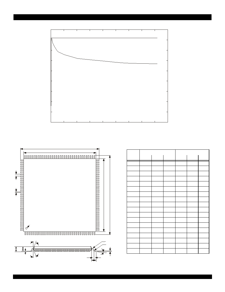
45 of 46
March 26, 2001
IDT77V012
Figure 50 Memory Usage for 11 Levels of Search (Continued)
3
3
3
3D
D
D
DF
F
F
FN
N
N
ND
D
D
DJH ,
JH ,
JH ,
JH ,Q
Q
Q
QIIIIR
R
R
RUUUUP
P
P
PD
D
D
DWLRQ
WLRQ
WLRQ
WLRQ
3O
3O
3O
3OD
D
D
DVVVVWWWWLF
LF
LF
LF 4)
4)
4)
4)3
3
3
3 S
S
S
SLQ
LQ
LQ
LQ %
%
%
%R
R
R
RG\ 6
G\ 6
G\ 6
G\ 6LLLL]]]]H
H
H
H [
[
[
[
[
[
[
[
PP
PP
PP
PP
0
500
1000
1500
2000
2500
3000
3500
4000
4500
0
2000
4000
6000
8000
10000
12000
14000
16000
18000
Number of search trees
N
u
m
b
e
r
o
f
c
o
n
n
e
c
t
i
o
n
s
256K memory - 32 bits header lookup - Cell accounting
Best Case
Worst Case
5347drw57
108
73
H
D
D
E
37
72
36
1
144
109
Index
b
f
H
E
A
2
A
1
A
m
a
x
R
1
R
C
L
2
L
L
1
q
2
q
q
3
5347drw58
Symbol Dimension in Millimeters
Dimension in Inches
1
1.
for reference
Min
Norm
Max
Min
Norm
Max
E
19.9
20
20.1
(0.784)
(0.787)
(0.791)
D
19.9
20
20.1
(0.784)
(0.787)
(0.791)
A
1.7
(0.066)
A1
0.1
(0.004)
A2
1.3
1.4
1.5
(0.052)
(0.055)
(0.059)
f
0.5
(0.020)
b
0.15
0.2
0.3
(0.006)
(0.008)
(0.011)
C
0.1
0.125
0.175
(0.004)
(0.005)
(0.006)
q
0o
10o
(0o)
(10o)
L
0.3
0.5
0.7
(0.012)
(0.020)
(0.027)
L1
1
(0.039)
L2
0.5
(0.020)
HE
21.6
22
22.4
(0.851)
(0.866)
(0.881)
HD
21.6
22
22.4
(0.851)
(0.866)
(0.881)
q2
12o
(12o)
q3
12o
(12o)
R
0.2
(0.008)
R1
0.2
(0.008)
46 of 46
March 26, 2001
IDT77V012
CORPORATE HEADQUARTERS
2975 Stender Way
Santa Clara, CA 95054
for SALES:
800-345-7015 or 408-727-6116
fax: 408-330-1748
www.idt.com
for Tech Support:
email: sarhelp@idt.com
phone: 408-492-8208
The IDT logo is a registered trademark of Integrated Device Technology, Inc.
2
2
2
2UUUUGHUL
GHUL
GHUL
GHULQ
Q
Q
QJ ,Q
J ,Q
J ,Q
J ,QIIIIR
R
R
RUUUUP
P
P
PD
D
D
DWLRQ
WLRQ
WLRQ
WLRQ
'
'
'
'D
D
D
DWD
WD
WD
WD 6K
6K
6K
6KHH
HH
HH
HHWWWW 'RFXPHQW +LVWR
'RFXPHQW +LVWR
'RFXPHQW +LVWR
'RFXPHQW +LVWRUUUU\\\\
9/07/99
Initial Public Release
10/26/99
Added Commercial temperature range and ordering information.
1/27/00
Added text to In-StreamTM section for 1 to 31-byte internal register access.
02/03/00
Fixed typos in In-StreamTM text.
03/03/00
Deleted Commercial temperature range and ordering information, corrected maximum delay values for back to back cells,
updated Utility bus write timing, corrected tables 25 and 32 In-StreamTM Direction.
09/12/00
Corrected In-StreamTM data field description and drawing for Notification cells.
10/15/00
Corrected text and drawings for In-StreamTM Discovery/Identify cells.
12/18/00
Converted from Preliminary to Final.
03/26/01
Added overbars to pin EECS; in Figure 12, changed
READ
to
RD
; in Note for Figure 46, added overbar to pins
CE
and
CS1
.
A
Power
999
Speed
A
Package
A
Process/
Temperature
Range
(Blank) Industrial
DA
PQFP (144-pin)
155
L
Low Power
XXXXX
Device
Type
DATA PATH INTERFACE (DPI) TO UTOPIA
LEVEL 1 HEADER TRANSLATION DEVICE
77V012
IDT
5347drw58
4-bit Port Bandwidth in Mbps