1 of 25
April 10, 2001
2001 Integrated Device Technology, Inc.
DSC 4952
Block diagram
Block diagram
Block diagram
Block diagram
The IDT logo is a registered trademark and RC32134, RC32364, RC64145, RC64474, RC64475, RC4650, RC4640, RC4600,RC4700 RC3081, RC3052, RC3051, RC3041, RISController, and RISCore are trade-
marks of Integrated Device Technology, Inc.
System Control
Coprocessor
(CPO )
Data Cache
(Lockable)
64-bit
330 M IPS
Instruction Cache
(Lockable)
16KB
16KB
RISCore4000
125 M FLO PS
Single/Double
FPA
32-/64-bit
Synchronized
System
Interface
Precision
C o n tro l B u s
In s tru ctio n B u s
D a ta B u s
CPU Core
Features
Features
Features
Features
x
High performance 64-bit microprocessor, based on the
RISCore4000
≠ Minimized branch and load delays, through streamlined
5-stage scalar pipeline.
≠ Single and double precision floating-point unit
≠ 125 peak MFLOP/s at 250 MHz
≠ 330 Dhrystone MIPS at 250 MHz
≠ Flexible RC4700-compatible MMU
≠ Joint TLB on-chip, for virtual-to-physical address mapping
x
On-chip two-way set associative caches
≠ 16KB instruction cache (I-cache)
≠ 16KB data cache (D-cache)
x
Optional I-cache and D-cache locking (per set), provides
improved real-time support
x
Enhanced, flexible bus interface allows simple, low-cost
design
≠ 64-bit Bus Interface option, 1000MB/s bandwidth support
≠ 32-bit Bus Interface option, 500MB/s bandwidth support
≠ SDRAM timing protocol, through delayed data in write cycles
≠ RC4000/RC5000 family bus-protocol compatibility
≠ Bus runs at fraction of pipeline clock (1/2 to 1/8)
x
Implements MIPS-III Instruction Set Architecture (ISA)
x
3.3V core with 3.3V I/O
x
Software compatible with entire RISController Series of
Embedded Microprocessors
x
Industrial temperature range support
x
Active power management
≠ Powers down inactive units, through sleep-mode feature
x
100% pin compatibility between RC64574, RC64474 and
RC4640
x
100% pin compatibility between RC64575, RC64475 and
RC4650
x
RC64474 available in 128-pin QFP package, for 32-bit only
systems
x
RC64475 available in 208-pin QFP package, for full 64/32 bit
systems
x
Simplified board-level testing, through full Joint Test Action
Group (JTAG) boundary scan
x
WindowsÆ CE compliant
RC64474
TM
RC64475
TM
RISController
TM
Embedded
64-bit Microprocessor, based on
RISCore4000
TM
2 of 25
April 10, 2001
RC64474TM RC64475TM
Device Overview
Device Overview
Device Overview
Device Overview
1
1
1
1
Extending Integrated Device Technology's (IDT) RISCore4000 based
choices (see Table 1), the RC64474 and RC64475 are high perfor-
mance 64-bit microprocessors targeted towards applications that require
high bandwidth, real-time response and rapid data processing and are
ideal for products ranging from internetworking equipment (switches,
routers) to multimedia systems such as web browsers, set-top boxes,
video games, and Windows
Æ
CE based products. These processors are
rated at 330 Dhrystone MIPS and 125 Million floating point operations
per second, at 250 MHz. The internal cache bandwidth for these devices
is over 3GB/second. The 64-bit external bus bandwidth is at more than
1000MB/s, and the 32-bit external bus bandwidth is at 500MB/s.
The RC64474 is packaged in a 128-pin QFP footprint package and
uses a 32-bit external bus, offering the ideal combination of 64-bit
processing power and 32-bit low-cost memory systems. The RC64475
is packaged in a 208-pin QFP footprint package and uses the full 64-bit
external bus. The RC64475 is ideal for applications requiring 64-bit
performance and 64-bit external bandwidth.
IDT's RISCore4000 is a 250MHz 64-bit execution core that uses a
5-stage pipeline, eliminating the "issue restrictions" associated with
other more complex pipelines. The RISCore4000 implements the
MIPS-III Instruction Set Architecture (ISA) and is upwardly compatible
with applications that run on earlier generation parts.
Implementation of the MIPS-III architecture results in 64-bit opera-
tions, improved performance for commonly used code sequences in
1.
Detailed system operation information is provided in the RC64474/RC64475
user's manual.
operating system kernels, and faster execution of floating-point intensive
applications.
The RISCore4000 integer unit implements a load/store architecture
with single cycle ALU operations (logical, shift, add, subtract) and an
autonomous multiply/divide unit. The ALU consists of the integer adder
and logic unit. The adder performs address calculations in addition to
arithmetic operations, and the logic unit performs all of the processor's
logical and shift operations. Each unit is highly optimized and can
perform an operation in a single pipeline cycle. Both 32- and 64-bit data
operations are performed by the RISCore4000, utilizing 32 general
purpose 64-bit registers (GPR) that are used for integer operations and
address calculation. A complete on-chip floating-point co-processor
(CP1), which includes a floating-point register file and execution units,
forms a "seamless" interface, decoding and executing instructions in
parallel with the integer unit.
CP1's floating-point execution units support both single and
double precision arithmetic--as specified in the IEEE Standard 754--
and are separated into a multiply unit and a combined add/convert/
divide/square root unit. Overlap of multiplies and add/subtract is
supported, and the multiplier is partially pipelined, allowing the initiation
of a new multiply instruction every fourth pipeline cycle.
The floating-point register file is made up of thirty-two 64-bit regis-
ters. The floating-point unit can take advantage of the 64-bit wide data
cache and issue a co-processor load or store doubleword instruction in
every cycle. The RISCore4000's system control coprocessor (CP0)
registers are also incorporated on-chip and provide the path through
which the virtual memory system's page mapping is examined and
changed, exceptions are handled, and any operating mode selections
are controlled.
RISCore4000/RISCore5000 Family of Socket Compatible Processors
RISCore4000/RISCore5000 Family of Socket Compatible Processors
RISCore4000/RISCore5000 Family of Socket Compatible Processors
RISCore4000/RISCore5000 Family of Socket Compatible Processors
Table 1 RISCore4000/RISCore5000 Processor Family
32-bit Processors
64-bit Processors
RC4640
RC64474
RC64574
RC4650
RC64475
RC64575
CPU
64-bit RISCore4000
w/ DSP extensions
64-bit RISCore4000
64-bit RISCore5000 w/
DSP extensions
64-bit RISCore4000
w/ DSP extensions
64-bit RISCore4000
64-bit RISCore5000
w/ DSP extensions
Performance
>350MIPS
>330MIPS
>440MIPS
>350MIPS
>330MIPS
>440MIPS
FPA
89 mflops, single pre-
cision only
125 mflops, single and
double precision
666 mflops, single and
double precision
89 mflops, single pre-
cision only
125 mflops, single
and double precision
666 mflops, single
and double precision
Caches
8kB/8kB, 2-way, lock-
able by set
16kB/16kB, 2-way,
lockable by set
32kB/32kB, 2-way,
lockable by line
8kB/8kB, 2-way, lock-
able by set
16kB/16kB, 2-way,
lockable by set
32kB/32kB, 2-way,
lockable by line
External Bus
32-bit
32-bit, Superset pin
compatible w/RC4640
32-bit, Superset pin
compatible w/RC4640,
RC64474
32- or 64-bit
32-or 64-bit, Super-
set pin compatible w/
RC4650
32-or 64-bit, Super-
set pin compatible w/
RC4650, RC64475
Voltage
3.3V
3.3V
2.5V
3.3V
3.3V
2.5V
Frequencies
100-267 MHz
180-250 MHz
200-333 MHz
100-267 MHz
180-250 MHz
200-333 MHz
Packages
128 PQFP
128 QFP
128 QFP
208 QFP
208 QFP
208 QFP
MMU
Base-Bounds
96 page TLB
96 page TLB
Base-Bounds
96 page TLB
96 page TLB
Key Features
Cache locking, on-
chip MAC, 32-bit
external bus
Cache locking, JTAG,
syncDRAM mode, 32-
bit external bus
Cache locking, JTAG,
syncDRAM mode, 32-
bit external bus
Cache locking, on-
chip MAC, 32-bit & 64
bit bus option
Cache locking, JTAG,
syncDRAM mode, 32-
64- bit bus option
Cache locking, JTAG,
syncDRAM mode, 32-
64- bit bus option
3 of 25
April 10, 2001
RC64474TM RC64475TM
A secure user processing environment is provided through the user,
supervisor, and kernel operating modes of virtual addressing to
system software. Bits in a status register determine which of these
modes is used.
If configured for 64-bit virtual addressing, the virtual address space
layout becomes an upwardly compatible extension of the 32-bit virtual
address space layout. Figure 1 is an illustration of the address space
layout for the 32-bit virtual address operation.
The RC64474/RC64475's Memory Management Unit (MMU)
controls the virtual memory system's page mapping and consists of a
translation lookaside buffer (TLB) used for the virtual memory-mapping
subsystem.
This large, fully associative TLB maps 96 virtual pages to their
corresponding physical addresses. The TLB is organized as 48 pairs of
even-odd entries and maps a virtual address and address space identi-
fier into the large, 64GB physical address space. To assist in controlling
the amount of mapped space and the replacement characteristics of
various memory regions, two mechanisms are provided. First, the page
size can be configured on a per-entry basis, to map a page size of 4KB
to 16MB (in increments of 4x).
The second mechanism controls the replacement algorithm, when a
TLB miss occurs. A random replacement algorithm is provided to select
a TLB entry to be written with a new mapping; however, the processor
provides a mechanism whereby a system specific number of mappings
0xFFFFFFFF
0xE0000000
Kernel virtual address space
(kseg3)
Mapped, 0.5GB
0xDFFFFFFF
Supervisor virtual address space
(sseg)
Mapped, 0.5GB
0xC0000000
0xBFFFFFFF
0xA0000000
Uncached kernel physical address space
(kseg1)
Unmapped, 0.5GB
0x9FFFFFFF
0x80000000
Cached kernel physical address space
(kseg0)
Unmapped, 0.5GB
0x7FFFFFFF
0x00000000
User virtual address space
(useg)
Mapped, 2.0GB
Figure 1 Kernel Mode Virtual Addressing (32-bit Mode)
can be locked into the TLB and avoid being randomly replaced, which
facilitates the design of real-time systems, by allowing deterministic
access to critical software.
The TLB also contains information to control the cache coherency
protocol, and cache management algorithm for each page. However,
hardware-based cache coherency is not supported.
The RC64474 and RC64475 enhance IDT's entire RISCore4000
series through the implementation of features such as boundary scan, to
facilitate board level testing; enhanced support for SyncDRAM, to
simplify system implementation and improve performance.
The RC64474/475 processors offer a direct migration path for
designs based on IDT's RC4640/RC4650 processors
2
, through full pin
and socket compatibility. Also, full 64-bit-family software and bus-
protocol compatibility ensures the RC64474/475 access to a robust
development tools infrastructure, allowing quicker time to market.
Development Tools
Development Tools
Development Tools
Development Tools
An array of hardware and software tools is available to assist system
designers in the rapid development of RC64474/475 based systems.
This accessibility allows a wide variety of customers to take full advan-
tage of the device's high-performance features while addressing today's
aggressive time-to-market demands.
Cache Memory
Cache Memory
Cache Memory
Cache Memory
To keep the RC64474 and RC64475's high-performance pipeline full
and operating efficiently, on-chip instruction and data caches have been
incorporated. Each cache has its own data path and can be accessed in
the same single pipeline clock cycle.
The 16KB two-way set associative instruction cache (I-cache) is
virtually indexed, physically tagged, and word parity protected. Because
this cache is virtually indexed, the virtual-to-physical address translation
occurs in parallel with the cache access, further increasing performance
by allowing both operations to occur simultaneously. The instruction
cache provides a peak instruction bandwidth of 1000MB/sec at 250MHz.
The 16KB two-way set associative data cache (D-cache) is byte
parity protected and has a fixed 32-byte (eight words) line size. Its tag is
protected with a single parity bit. To allow simultaneous address transla-
tion and data cache access, the D-cache is virtually indexed and physi-
cally tagged. The data cache can provide 8 bytes each clock cycle, for a
peak bandwidth of 2GB/sec.
To lock critical sections of code and/or data into the caches for quick
access, a "cache locking" feature has been implemented. Once
enabled, a cache is said to be locked when a particular piece of code or
data is loaded into the cache and that cache location will not be selected
later for refill by other data. This feature locks a set (8KB) of Instructions
and/or Data.
Table 2 lists the RC64474/475 Instruction and data cache attributes.
2.
To ensure socket compatibility, refer to Table 8 and Table 9 at back of data
sheet.
4 of 25
April 10, 2001
RC64474TM RC64475TM
Table 2 RC64474/RC64475 Instruction/Data Cache Attributes
System Interfaces
System Interfaces
System Interfaces
System Interfaces
The RC64475 supports a 64-bit system interface that is bus compat-
ible with the RC4650 and RC64575 system interface. The system inter-
face consists of a 64-bit Address/Data bus with 8 check bits and a 9-bit
command bus that is parity protected.
During 64-bit operation, RC64475 system address/data (SysAD)
transfers are protected with an 8-bit parity check bus, SysADC. When
initialized for 32-bit operation, the RC64475's SysAD can be viewed as a
32-bit multiplexed bus that is protected by 4 parity check bits.
The RC64474 supports a 32-bit system interface that is bus compat-
ible with the RC4640. During 32-bit operation, SysAD transfers are
performed on a 32-bit multiplexed bus (SysAD 31:0) that is protected by
4 parity check bits (SysADC 6:0).
Writes to external memory--whether they are cache miss write-
backs, stores to uncached or write-through addresses--use the on-chip
write buffer. The write buffer holds a maximum of four 64-bit addresses
and 64-bit data pairs. The entire buffer is used for a data cache write-
back and allows the processor to proceed in parallel with memory
updates.
Included in the system interface are six handshake signals:
RdRdy*, WrRdy*, ExtRqst*, Release*, ValidOut*, and ValidIn*; six inter-
rupt inputs, and a simple timing specification that is capable of trans-
ferring data between the processor and memory at a peak rate of
1000MB/sec. A boot-time selectable option to run the system interface
as 32-bits wide--using basically the same protocols as the 64-bit
system--is also supported.
Characteristics
Instruction
Data
Size
16KB
16KB
Organization
2-way set
associative
2-way set
associative
Line size
32B
32B
read unit
32-bits
64-bits
write policy
na
write-back, write-through
with or without write-allocate
Line transfer order
sub-block order,
for refill
sub-block order, for load
sequential order, for store
Miss restart
after transfer of:
entire line
miss word
Parity
per-word
per-byte
Cache locking
per set
per set
A boot-time mode control interface initializes fundamental
processor modes. The boot-time mode control interface is a serial inter-
face that operates at a very low frequency (MasterClock divided by
256). This low-frequency operation allows the initialization information to
be kept in a low-cost EPROM; alternatively, the twenty-or-so bits could
be generated by the system interface ASIC or a simple PAL. The boot-
time serial stream and configuration options are listed in Table 3.
The clocking interface allows the CPU to be easily mated with
external reference clocks. The CPU input clock is the bus reference
clock and can be between 25 and 125MHz. An on-chip phase-locked-
loop (PLL) generates the pipeline clock (PClock) through multiplication
of the system interface clock by values of 2,3,4,5,6,7 or 8, as defined at
system reset. This allows the pipeline clock to be implemented at a
significantly higher frequency than the system interface clock. The
RC64474/475 support single data (one to eight bytes) and 8-word block
transfers on the SysAD bus.
The RC64474/475 implement additional write protocols that
double the effective write bandwidth. The write re-issue has a repeat
rate of 2 cycles per write. Pipelined writes have the same 2-cycle per
write repeat rate, but can issue an additional write after WrRdy* de-
asserts.
Choosing a 32- or 64-bit wide system interface dictates whether a
cache line block transaction requires 4 double word data cycles or 8
single word cycles as well as whether a single data transfer--larger than
4 bytes--must be divided into two smaller transfers.
Board-level testing during Run-Time mode is facilitated through the
full JTAG boundary scan facility. Six pins--TDI, TDO, TMS, TCK, TRST*
and JTAG32*--have been incorporated to support the standard JTAG
interface.
System Enhancement
System Enhancement
System Enhancement
System Enhancement
To facilitate discrete interface to SDRAM, the RC64474/475 bus
interface is enhanced during write cycles with a programmable delay
that is inserted between the write address and the write data (for both
block and non-block writes).
The bus delay can be defined as 0 to 7 MasterClock cycles and is
activated and controlled through mode bit (17:15) settings selected
during the reset initialization sequence. The `000' setting provides the
same write operations timing protocol as the RC4640, RC4650, and
RC5000 processors.

5 of 25
April 10, 2001
RC64474TM RC64475TM
Serial
Bit
Description
Value & Mode Setting
255:18
Reserved
Must be 0
17:15
WAdrWData_Del
Write address to write data delay in Master-
Clock cycles.Æ
000
0 cycles
001
1 cycle
010
2 cycles
011
3 cycles
100
4 cycles
101
5 cycles
110
6 cycles
111
7 cycles
14:13
Drv_Out
output driver slew rate control. Bit 14 is MSB.
Affects only non-clock outputs.
Output driver strength:
10
100% strength (fastest)
11
83% strength
00
67% strength
01
50% strength (slowest)
12
System interface bus width
0
64-bit system interface
1
32-bit system interface
11
TmrIntEn
Disables the timer interrupt on Int*[5]
0
Enabled Timer Interrupt
1
Disabled Timer Interrupt
10:9
Non-block write
Selects non-block write type. Bit 10 is MSB.
00
RC4x00 compatible
01
Reserved
10
Pipelined writes
11
Write re-issue
7:5
Clock
Multiplier
MasterClock is multiplied internally to gener-
ate PClock
Clock multiplier:
0 Multiply by 2
1 Multiply by 3
2 Multiply by 4
3 Multiply by 5
4 Multiply by 6
5 Multiply by 7
6 Multiply by 8
7 Reserved
8
EndBit
Specifies byte ordering
0
Little endian
1
Big endian
4:1
Writeback data rate
System interface data rate for block writes
only: bit 4 is MSB
64-bit:
9:15 Reserved
8
dxxxdxxxdxxxdxxx
7
ddxxxxxxddxxxxxx
6
dxxdxxdxxdxx
5
ddxxxxddxxxx
4
ddxxxddxxx
3
dxdxdxdx
2
ddxxddxx
1
ddxddx
0
dddd
32-bit:
9:15 Reserved
8
wxxxwxxxwxxxwxxxwxxxwxxxwxxxwxxx
7
wwxxxxxxwwxxxxxxwwxxxxxxwwxxxxxx
6
wxxwxxwxxwxxwxxwxxwxxwxx
5
wwxxxxwwxxxxwwxxxxwwxxxx
4
wwxxxwwxxxwwxxxwwxxx
3
wxwxwxwxwxwxwxwx
2
wwxxwwxxwwxxwwxx
1
wwxwwxwwxwwx
0
∆ wwwwwwww
0
Reserved
Must be zero
Table 3 Boot-time Mode Stream
6 of 25
April 10, 2001
RC64474TM RC64475TM
Power Management
Power Management
Power Management
Power Management
Executing the WAIT instruction enables the processor to enter
Standby mode. The internal clocks will shut down, thus freezing the
pipeline. The PLL, internal timer, and some of the input pins (Int[5:0]*,
NMI*, ExtReq*, Reset*, and ColdReset*) will continue to run. Once the
CPU is in Standby Mode, any interrupt, including the internally gener-
ated timer interrupt, will cause the CPU to exit Standby Mode.
Thermal Considerations
Thermal Considerations
Thermal Considerations
Thermal Considerations
The RC64474/475 come in a QFP with a drop-in heat spreader and
are guaranteed in a case temperature range of 0
∞
to +85
∞
C, for
commercial temperature devices; - 40
∞
to +85
∞
for industrial tempera-
ture devices. The type of package, speed (power) of the device, and
airflow conditions affect the equivalent ambient temperature conditions
that will meet this specification.
The equivalent allowable ambient temperature, T
A
, can be calculated
using the thermal resistance from case to ambient (
CA
) of the given
package. The following equation relates ambient and case tempera-
tures:
T
A
= T
C
- P *
CA
where P is the maximum power consumption at hot temperature,
calculated by using the maximum I
CC
specification for the device.
Typical values for
CA
at various airflows are shown in Table 4. Note
that the RC64474/475 processors implement advanced power manage-
ment, which substantially reduces the typical power dissipation of the
device.
Data Sheet Revision History
Data Sheet Revision History
Data Sheet Revision History
Data Sheet Revision History
December 1998: Changed ordering code on 128-pin package from
DQ / DQI (Industrial) to DZ / DZI (Industrial).
January 1999: Removed 5V tolerance capability and deleted 5V
tolerant pin.
February 1999: Changed the package drawings to reflect the new
208-pin DP (DPI) and 128-pin DZ (DZI) packages.
May 1999: Removed "Preliminary" status from data sheet.
Changes in DC Electrical Characteristics table. Changes in Pin
Description table. Changes in Clock Parameters table. Changes in
System Interface Parameters table.
September 1999: Updated Revision History section.
CA
Airflow (ft/min)
0
200 400 600 800 1000
128 QFP
16
10
9
7
6
5
208 QFP
20
13
10
9
8
7
Table 4 Thermal Resistance (
CA) at Various Airflows
January 17, 2000: Added "with DSP extensions" in the CPU row
under RC64574 and RC64575 columns in Table 1. Added "lockable by
line" in the Caches row under RC64574 and RC64575 columns in Table
1. Revised Data Output and Data Output Hold rows in System Interface
Parameters table.
February 10, 2000: Revised values in Table 4, Thermal Resistance.
Old values were:
March 13, 2000: Replaced existing figure in Mode Configuration
Interface Reset Sequence section with 3 reset figures.
March 28, 2000: Removed the symbol t
DZ
from Figure 3.
April 17, 2000: Changed V
IH
value in 200MHz column from 2.0V to
0.7V
CC
.
April 10, 2001: In the Data Output and Data Output Hold categories
of the System Interface Parameters table, changed values in the Min
column for all speeds from 1.0 to 0. Deleted Output for Loading AC
Testing diagram and added Output Loading for AC Timing diagram
(Figure 8).
CA
Airflow (ft/min)
0
200 400 600 800 1000
128 QFP
20
12
9
8
7
6
208 QFP
20
12
9
8
7
6
7 of 25
April 10, 2001
RC64474TM RC64475TM
Pin Description Table
Pin Description Table
Pin Description Table
Pin Description Table
The following is a list of system interface pins available on the RC64474/475. Pin names ending with an asterisk (*) are active when low.
Pin Name
Type
Description
System Interface
ExtRqst*
I
External request
An external agent asserts ExtRqst* to request use of the System interface. The processor grants the request by asserting
Release*.
Release*
O
Release interface
In response to the assertion of ExtRqst* or a CPU read request, the processor asserts Release* and signals to the request-
ing device that the system interface is available.
RdRdy*
I
Read Ready
The external agent asserts RdRdy* to indicate that it can accept a processor read request.
WrRdy*
I
Write Ready
An external agent asserts WrRdy* when it can now accept a processor write request.
ValidIn*
I
Valid Input
Signals that an external agent is now driving a valid address or data on the SysAD bus and a valid command or data iden-
tifier on the SysCmd bus.
ValidOut*
O
Valid output
Signals that the processor is now driving a valid address or data on the SysAD bus and a valid command or data identifier
on the SysCmd bus.
SysAD(63:0)
I/O
System address/data bus
A 64-bit address and data bus for communication between the processor and an external agent. During address phases
only, SysAd(35:0) contains valid address information. The remaining SysAD(63:36) pins are not used. The whole 64-bit
SysAD(63:0) may be used during the data transfer phase.
In 32-bit mode and in the RC64474, SysAD(63:32) is not used, regardless of Endianness. A 32-bit address and data com-
munication between processor and external agent is performed via SysAD(31:0).
SysADC(7:0)
I/O
System address/data check bus
An 8-bit bus containing parity check bits for the SysAD bus during data bus cycles.
In 32-bit mode and in the RC64474, SysADC(7:4) is not used. The SysADC(3:0) contains check bits for SysAD(31:0).
SysCmd(8:0)
I/O
System command/data identifier bus
A 9-bit bus for command and data identifier transmission between the processor and an external agent.
SysCmdP
I/O
System Command Parity
A single, even-parity bit for the Syscmd bus. This signal is always driven low.
Clock/Control Interface
MasterClock
I
Master Clock
Master clock input establishes the processor and bus operating frequency. It is multiplied internally by 2,3,4,5,6,7,8 to gen-
erate the pipeline clock (PClock). This clock must be driven by 3.3V (Vcc) clock signals, regardless of the 5V tolerant pin
setting.
V
CC
P
I
Quiet VCC for PLL
Quiet V
CC
for the internal phase locked loop.
V
SS
P
I
Quiet V
SS
for PLL
Quiet V
SS
for the internal phase locked loop.
Interrupt Interface
Int*(5:0)
I
Interrupt
Six general processor interrupts, bit-wise ORed with bits 5:0 of the interrupt register.
Table 5 Pin Descriptions (Page 1 of 2)
8 of 25
April 10, 2001
RC64474TM RC64475TM
NMI*
I
Non-maskable interrupt
Non-maskable interrupt, ORed with bit 6 of the interrupt register.
Initialization Interface
V
CC
O
k
I
V
CC
is OK
When asserted, this signal indicates to the processor that the power supply has been above the Vcc minimum for more
than 100 milliseconds and will remain stable. The assertion of V
CCO
k initiates the initialization sequence.
ColdReset*
I
Cold reset
This signal must be asserted for a power on reset or a cold reset. ColdReset must be de-asserted synchronously with Mas-
terClock.
Reset*
I
Reset
This signal must be asserted for any reset sequence. It can be asserted synchronously or asynchronously for a cold reset,
or synchronously to initiate a warm reset. Reset must be de-asserted synchronously with MasterClock.
ModeClock
O
Boot-mode clock
Serial boot-mode data clock output at the system clock frequency divided by two hundred fifty-six.
ModeIn
I
Boot-mode data in
Serial boot-mode data input.
JTAG Interface
TDI
I
JTAG Data In
On the rising edge of TCK, serial input data are shifted into either the Instruction register or Data register, depending on the
TAP controller state.
TDO
O
JTAG Data Out
On the falling edge of TCK, the TDO is serial data shifted out from either the instruction or data register. When no data is
shifted out, the TDO is tri-stated (high impedance).
TCK
I
JTAG Clock Input
An input test clock used to shift into or out of the boundary-scan register cells. TCK is independent of the system and pro-
cessor clock with nominal 40-60% duty cycle.
TMS
I
JTAG Command Select
The logic signal received at the TMS input is decoded by the TAP controller to control test operation. TMS is sampled on
the rising edge of TCK.
TRST*
I
JTAG Reset
The TRST* pin is an active-low signal used for asynchronous reset of the debug unit, independent of the processor logic.
During normal CPU operation, the JTAG controller will be held in the reset mode, asserting this active low pin.
When asserted low, this pin will also tristate the TDO pin.
JTAG32*
I
JTAG 32-bit scan
This pin is used to control length of the scan chain for SYsAD (32-bit or 64-bit) for the JTAG mode. When set to Vss, 32-bit
bus mode is selected. In this mode, only SysAD(31:0) are part of the scan chain. When set to Vcc, 64-bit bus mode is
selected. In this mode, SysAD(63:0) are part of the scan chain. This pin has a built-in pull-down device to guarantee 32-bit
scan, if it is left uncovered.
JR_Vcc
I
JTAG VCC
This pin has an internal pull-down to continuously reset the JTAG controller (if left unconnected) bypassing the TRst* pin.
When supplied with Vcc, the TRst* pin will be the primary control for the JTAG reset.
Pin Name
Type
Description
Table 5 Pin Descriptions (Page 2 of 2)

9 of 25
April 10, 2001
RC64474TM RC64475TM
Logic Diagram -- RC64474/RC64475
Logic Diagram -- RC64474/RC64475
Logic Diagram -- RC64474/RC64475
Logic Diagram -- RC64474/RC64475
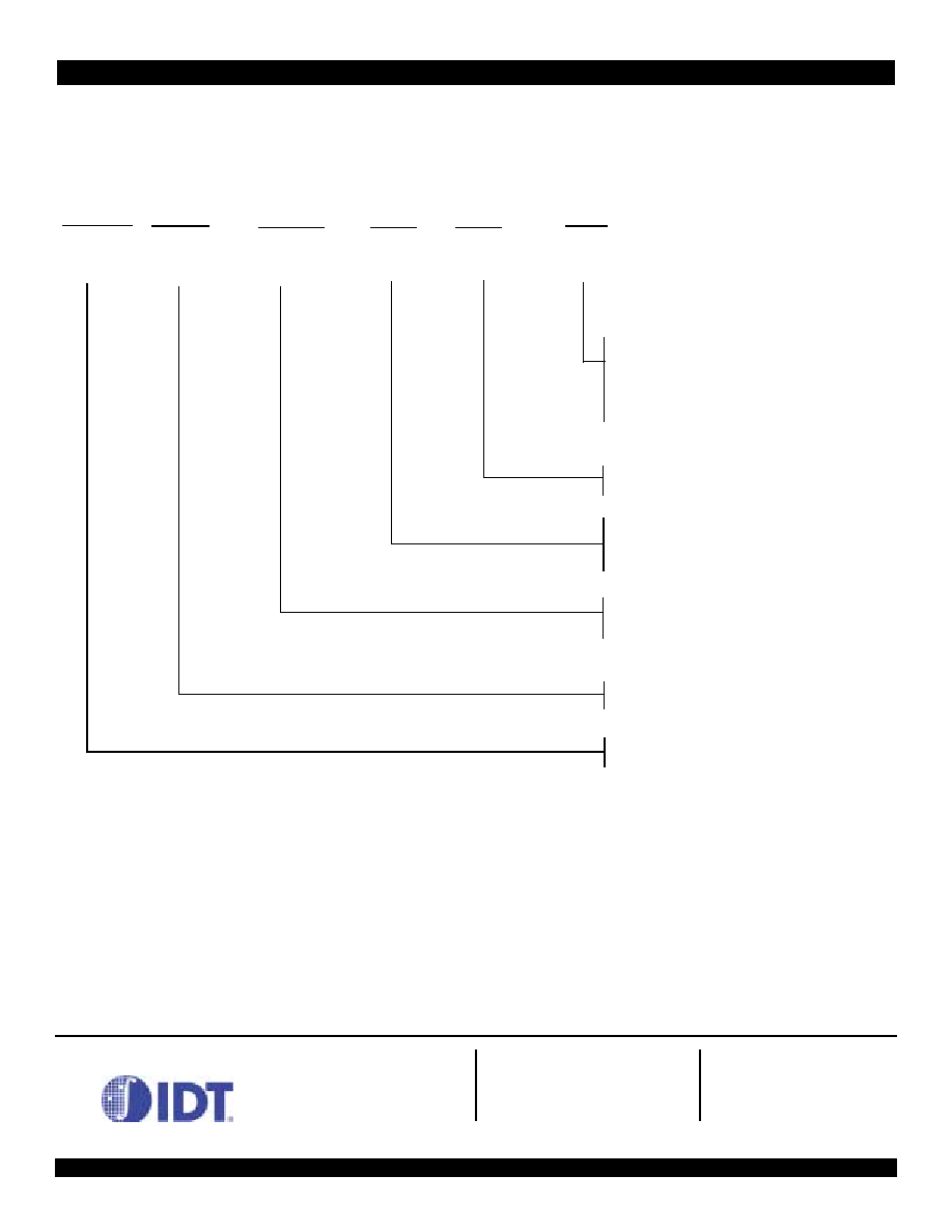
Figure 2 illustrates the direction and functional groupings for the processor signals.
Figure 2 Logic Diagram for RC64474/RC64475
SysAD(63:0)
MasterClock
ColdReset*
Reset*
V
CC
P
V
SS
P
Initi
a
lization
Interface
Interr
upt
S
ystem Interface
Cl
ock/Control Interface
RC64474/
Logic
Symbol
64
6
Interface
SysADC(7:0)
8
NMI
*
Int*(5:0)
JT
AG
Interfa
c
e
TDI
TMS
TRST*
TDO
Handshake
S
i
gnals
RC64475
TCK
RdRdy*
WrRdy*
ExtRqst*
Release*
ValidIn*
ValidOut*
SysCmd(8:0)
SysCmdP
9
VCCOK
ModeClock
ModeIn
JTag32*
JR_Vcc
10 of 25
April 10, 2001
RC64474TM RC64475TM
RC64475 208-pin QFP Package Pin-out
RC64475 208-pin QFP Package Pin-out
RC64475 208-pin QFP Package Pin-out
RC64475 208-pin QFP Package Pin-out
Pin names followed by an asterisk (*) are active when low. For maximum flexibility and compatibility with future designs, N.C. pins should be left
floating.
Pin
Function
Pin
Function
Pin
Function
Pin
Function
1
N.C.
53
JTAG32*
105
N.C.
157
N.C.
2
N.C.
54
N.C.
106
N.C.
158
N.C.
3
N.C.
55
N.C.
107
N.C.
159
SysAD59
4
N.C.
56
N.C.
108
N.C.
160
ColdReset*
5
N.C.
57
SysCmd2
109
N.C.
161
SysAD28
6
N.C.
58
SysAD36
110
N.C.
162
VCC
7
N.C.
59
SysAD4
111
N.C.
163
V
SS
8
N.C.
60
SysCmd1
112
N.C.
164
SysAD60
9
N.C.
61
V
SS
113
N.C.
165
Reset*
10
SysAD11
62
V
cc
114
SysAD52
166
SysAD29
11
V
SS
63
SysAD35
115
ExtRqst*
167
SysAD61
12
V
cc
64
SysAD3
116
V
cc
168
SysAD30
13
SysCmd8
65
SysCmd0
117
V
SS
169
V
cc
14
SysAD42
66
SysAD34
118
SysAD21
170
V
SS
15
SysAD10
67
V
SS
119
SysAD53
171
SysAD62
16
SysCmd7
68
V
cc
120
RdRdy*
172
SysAD31
17
V
SS
69
SysAD2
121
Modein
173
SysAD63
18
V
cc
70
Int5*
122
SysAD22
174
V
cc
19
SysAD41
71
SysAD33
123
SysAD54
175
V
SS
20
SysAD9
72
SysAD1
124
V
cc
176
V
cc
OK
21
SysCmd6
73
V
SS
125
V
SS
177
SysADC3
22
SysAD40
74
V
cc
126
Release*
178
SysADC7
23
V
SS
75
Int4*
127
SysAD23
179
N.C.
24
V
cc
76
SysAD32
128
SysAD55
180
TDI
25
SysAD8
77
SysAD0
129
NMI*
181
TRst*
26
SysCmd5
78
Int3*
130
V
cc
182
TCK
27
SysADC4
79
V
SS
131
V
SS
183
TMS
28
SysADC0
80
V
cc
132
SysADC2
184
TDO
29
V
SS
81
Int2*
133
SysADC6
185
V
cc
P
30
V
cc
82
SysAD16
134
SysAD24
186
V
SS
P
31
SysCmd4
83
SysAD48
135
V
cc
187
MasterClock
32
SysAD39
84
Int1*
136
V
SS
188
V
cc
33
SysAD7
85
V
SS
137
SysAD56
189
V
SS
Table 6 RC64475 208-pin QFP Package Pin-Out (Page 1 of 2)
11 of 25
April 10, 2001
RC64474TM RC64475TM
RC64474 128-pin QFP Package Pin-out
RC64474 128-pin QFP Package Pin-out
RC64474 128-pin QFP Package Pin-out
RC64474 128-pin QFP Package Pin-out
34
SysCmd3
86
V
cc
138
SysAD25
190
SysADC5
35
V
SS
87
SysAD17
139
SysAD57
191
SysADC1
36
V
cc
88
SysAD49
140
N.C.
192
V
cc
37
SysAD38
89
Int0*
141
V
SS
193
V
SS
38
SysAD6
90
SysAD18
142
N.C
194
SysAD47
39
ModeClock
91
V
SS
143
SysAD26
195
SysAD15
40
WrRdy*
92
V
cc
144
SysAD58
196
SysAD46
41
SysAD37
93
SysAD50
145
N.C.
197
V
cc
42
SysAD5
94
ValidIn*
146
V
cc
198
V
SS
43
V
SS
95
SysAD19
147
V
SS
199
SysAD14
44
V
cc
96
SysAD51
148
SysAD27
200
SysAD45
45
N.C.
97
V
SS
149
N.C.
201
SysAD13
46
N.C.
98
V
cc
150
JR_
V
cc
202
SysAD44
47
N.C.
99
ValidOut*
151
N.C.
203
V
SS
48
N.C.
100
SysAD20
152
N.C.
204
V
cc
49
N.C.
101
N.C.
153
N.C.
205
SysAD12
50
N.C.
102
N.C.
154
N.C.
206
SysCmdP
51
N.C.
103
N.C.
155
N.C.
207
SysAD43
52
N.C.
104
N.C.
156
N.C.
208
N.C.
Pin
Function
Pin
Function
Pin
Function
Pin
Function
1
JTAG32*
33
V
cc
65
V
cc
97
Vcc
2
SysCmd2
34
Vss
66
SysAD28
98
Vss
3
Vcc
35
SysAD13
67
ColdReset*
99
SysAD19
4
Vss
36
SysAD14
68
SysAD27
100
ValidIn*
5
SysAD5
37
Vss
69
Vss
101
Vcc
6
WrRdy*
38
Vcc
70
Vcc
102
Vss
7
ModeClock
39
SysAD15
71
JR_Vcc
103
SysAD18
8
SysAD6
40
Vss
72
SysAD26
104
Int0*
9
Vcc
41
Vcc
73
N.C.
105
SysAD17
10
Vss
42
SysADC1
74
Vss
106
Vcc
11
SysCmd3
43
Vss
75
N.C.
107
Vss
12
SysAd7
44
Vcc
76
SysAD25
108
Int1*
13
SysCmd4
45
MasterClock
77
Vss
109
SysAD16
Table 7 RC64474 128-pin QFP Package Pin-out (Page 1 of 2)
Pin
Function
Pin
Function
Pin
Function
Pin
Function
Table 6 RC64475 208-pin QFP Package Pin-Out (Page 2 of 2)
12 of 25
April 10, 2001
RC64474TM RC64475TM
Socket Compatibility--RC64474 & RC4640
Socket Compatibility--RC64474 & RC4640
Socket Compatibility--RC64474 & RC4640
Socket Compatibility--RC64474 & RC4640
To ensure socket compatibility between the RC4640 and the RC64474 devices, several pin changes are required, as shown below.
14
Vcc
46
VssP
78
Vcc
110
Int2*
15
Vss
47
VccP
79
SysAD24
111
Vcc
16
SysAdC0
48
TDO
80
SysADC2
112
Vss
17
SysCmd5
49
TMS
81
Vss
113
Int3*
18
SysAD8
50
TCK
82
Vcc
114
SysAD0
19
Vcc
51
TRst*
83
NMI*
115
Int4*
20
Vss
52
TDI
84
SysAD23
116
Vcc
21
SysCmd6
53
Vss
85
Release*
117
Vss
22
SysAD9
54
SysADC3
86
Vss
118
SysAD1
23
Vcc
55
VccOK
87
Vcc
119
Int5*
24
Vss
56
Vss
88
SysAD22
120
SysAD2
25
SysCCmd7
57
Vcc
89
Modein
121
Vcc
26
SysAD10
58
SysAD31
90
RdRdy*
122
Vss
27
SysCmd8
59
Vss
91
SysAD21
123
SysCmd0
28
Vcc
60
Vcc
92
Vss
124
SysAd3
29
Vss
61
SysAD30
93
Vcc
125
Vcc
30
SysAD11
62
SysAD29
94
ExtRqst*
126
Vss
31
SysCmdP
63
Reset*
95
SysAD20
127
SysCmd1
32
SysAD12
64
Vss
96
ValidOut*
128
SysAD4
Pin
RC4640
RC64574/
RC64474
Compatible to
RV4640?
Comments
1
N.C
JTAG32*
Yes.
Pin has an internal pull-down, to enable 32-bit scan.
Can also be left a N.C.
48
V
ss
TDO
Yes.
Can be driven with V
ss
, if JTAG is not needed. Is tristated when TRst* is low.
49
V
ss
TMS
Yes.
Can be driven with V
ss
if JTAG is not needed.
50
V
ss
TCK
Yes.
Can be driven with V
ss
if JTAG is not needed.
51
V
ss
TRst*
Yes.
Can be driven with V
ss
if JTAG is not needed.
52
V
ss
TDI
Yes.
Can be driven with V
ss
if JTAG is not needed.
71
N.C.
JR_V
cc
Yes.
Can be left N.C. in RC64474, if JTAG is not need. If JTAG is needed, it must
be driven to V
cc
.
Table 8 RC64574 Socket Compatibility to RC64474 and R4640
Pin
Function
Pin
Function
Pin
Function
Pin
Function
Table 7 RC64474 128-pin QFP Package Pin-out (Page 2 of 2)
13 of 25
April 10, 2001
RC64474TM RC64475TM
Socket Compatibility--RC64475 & RC4650
Socket Compatibility--RC64475 & RC4650
Socket Compatibility--RC64475 & RC4650
Socket Compatibility--RC64475 & RC4650
Absolute Maximum Ratings
Absolute Maximum Ratings
Absolute Maximum Ratings
Absolute Maximum Ratings
Note:
Stresses greater than those listed under ABSOLUTE MAXIMUM RATINGS may cause permanent damage to the device. This is a stress rating only and functional
operation of the device at these or any other conditions above those indicated in the operational sections of this specification is not implied. Exposure to absolute maximum
rating conditions for extended periods may affect reliability.
Recommended Operation Temperature and Supply Voltage
Recommended Operation Temperature and Supply Voltage
Recommended Operation Temperature and Supply Voltage
Recommended Operation Temperature and Supply Voltage
Pin
RV4650
32-bit
RC64575
32-bit
RC64475
32-bit
RV4650
64-bit
RC64575
64-bit
RC64475
64-bit
Compatible
to RV4650?
Comments
53
N.C.
JTAG32*
No Connect
JTAG32*
Yes
In 32-bit, this pin can be left unconnected
because of internal pull-down.
In 64-bit, this assumes that JTAG will not be
used. If using JTAG, this pin must be at V
cc
.
150
N.C.
JR_V
cc
No Connect
JR_V
cc
Yes
In RC64475, can be left a N.C, if JTAG is not
need. If JTAG is needed, it must be driven to
V
cc
.
180
N.C.
TDI
No Connect
TDO
Yes
If JTAG is not needed, can be left a N.C.
181
N.C.
TRsT*
No Connect
TRsT*
Yes
If JTAG is not needed, can be left a N.C.
182
N.C.
TCK
No Connect
TCK
Yes
If JTAG is not needed, can be left a N.C.
183
N.C.
TMS
No Connect
TMS
Yes
If JTAG is not needed, can be left a N.C.
184
N.C.
TDO
No Connect
TDIO
Yes
If JTAG is not needed, can be left a N.C.
Table 9 RC64575 Socket Compatibility to RC64475 & RC4650
Symbol
Rating
RC64474/475
3.3V±5%
RC64474/475
3.3V±5%
Unit
Commercial
Industrial
V
TERM
Terminal Voltage with respect to GND
≠0.5
1
to +4.6
1.
V
IN
minimum = ≠2.0V for pulse width less than 15ns. V
IN
should not exceed V
CC
+0.5 Volts.
≠0.5
1
to +4.6
V
T
C
Operating Temperature(case)
0 to +85
-40 to +85
∞
C
T
BIAS
Case Temperature Under Bias
≠55 to +125
≠55 to +125
∞
C
T
STG
Storage Temperature
≠55 to +125
≠55 to +125
∞
C
I
IN
DC Input Current
20
2
2.
When V
IN
< 0V or V
IN
> V
CC
20
2
mA
I
OUT
DC Output Current
50
3
3.
Not more than one output should be shorted at a time. Duration of the short should not exceed 30 seconds.
50
3
mA
Grade
Temperature
Gnd
RC64474/475
V
CC
Commercial
0
∞
C to +85
∞
C (Case)
0V
3.3V±5%
Industrial
-40 + 85
∞
C (Case)
0V
3.3V±5%
14 of 25
April 10, 2001
RC64474TM RC64475TM
DC Electrical Characteristics
DC Electrical Characteristics
DC Electrical Characteristics
DC Electrical Characteristics
Commercial Temperature Range--RC64474/64475
(V
CC
= 3.3
±
5
%, T
CASE
= 0
∞
C to +85
∞
C)
Power Consumption--RC64474
Power Consumption--RC64474
Power Consumption--RC64474
Power Consumption--RC64474
.
Parameter
RC64474/RC64475
180MHz
RC64474/RC64475
200MHz
RC64474/RC64475
250MHz
Conditions
Minimum
Maximum
Minimum
Maximum Minimum Maximum
V
OL
--
0.1V
--
0.1V
--
0.1V
|I
OUT
|= 20uA
V
OH
V
CC
- 0.1V
--
V
CC
- 0.1V
--
V
CC
- 0.1V
--
V
OL
--
0.4V
--
0.4V
--
0.4V
|I
OUT
|= 4mA
V
OH
2.4V
--
2.4V
--
2.4V
--
V
IL
≠0.5V
0.2V
CC
≠0.5V
0.2V
CC
≠0.5V
0.2V
CC
--
V
IH
2.0V
V
CC
+ 0.5V
0.7V
CC
V
CC
+ 0.5V
2.0V
V
CC
+ 0.5V
--
I
IN
--
±10uA
--
±10uA
--
±10uA
0
V
IN
V
CC
C
IN
--
10pF
--
10pF
--
10pF
--
C
OUT
--
10pF
--
10pF
--
10pF
--
I/O
LEAK
--
20uA
--
20uA
--
20uA
Input/Output Leakage
Parameter
RC64474 180MHz
RC64474 200MHz
RC64474 250MHz
Conditions
Typical
1
1.
Typical integer instruction mix and cache miss rates
Max
Typical
1
Max
Typical
1
Max
System Condition:
180/90MHz
200/100MHz
250/125MHz
--
I
CC
standby
--
60 mA
2
2.
These are not tested. They are the results of engineering analysis and are provided for reference only
--
60 mA
2
--
100 mA
2
C
L
= 0pF
3
3.
Guaranteed by design.
--
110 mA
2
--
110 mA
2
--
110 mA
2
C
L
= 50pF
active
530 mA
2
630 mA
2
600mA
2
700 mA
2
700 mA
2
850mA
2
C
L
= 0pF
No SysAd activity
3
630mA
2
750 mA
2
700 mA
2
850 mA
2
850mA
2
1000mA
2
C
L
= 50pF
R4x00 compatible writes,
T
C
= 25
o
C
750 mA
2
1050 mA
4
4.
These are the specifications IDT tests to insure compliance.
850 mA
2
1200 mA
4
1000mA
2
1400mA
2
C
L
= 50pF
Pipelined writes or write
re-issue,
T
C
= 25
o
C
3
15 of 25
April 10, 2001
RC64474TM RC64475TM
Power Consumption--RC64475
Power Consumption--RC64475
Power Consumption--RC64475
Power Consumption--RC64475
Timing Characteristics--RC64474/RC64475
Timing Characteristics--RC64474/RC64475
Timing Characteristics--RC64474/RC64475
Timing Characteristics--RC64474/RC64475
Figure 3 System Clocks Data Setup, Output, and Hold Timing
Parameter
RC64475 180MHz
RC64475 200MHz
RC64475 250MHz
Conditions
Typical
1
1.
Typical integer instruction mix and cache miss rates
Max
Typical
1
Max
Typical
1
Max
System Condition:
180/90MHz
200/100MHz
250/125MHz
--
I
CC
standby
--
60 mA
2
2.
These are not tested. They are the results of engineering analysis and are provided for reference only.
--
60 mA
2
--
100 mA
2
C
L
= 0pF
3
3.
Guaranteed by design.
--
110 m
2
A
--
110 mA
2
--
110 mA
2
C
L
= 50pF
active,
64-bit bus
option
4
4.
In 32-bit bus option, use RC64474 power consumption values.
720 mA
2
850 mA
2
850 mA
2
1000 mA
2
935 mA
2
1100 mA
2
C
L
= 0pF
No SysAd activity
3
850 mA
2
1000 mA
2
1000 mA
2
1200 mA
2
1100mA
2
1360mA
2
C
L
= 50pF
R4x00 compatible writes,
T
C
= 25
o
C
1000 mA
2
1200 mA
5
5.
These are the specifications IDT tests to insure compliance.
1200 mA
2
1400 mA
5
1360 mA
2
1600 mA
2
C
L
= 50pF
Pipelined writes or write re-issue,
T
C
= 25
o
C
3
Cycle
1
2
3
4
MasterClock
t
MCkHigh
t
MCkLow
t
MCkP
SysAD,SysCmd Driven
D
D
D
t
DM
t
DO
SysAD,SysCmd Received
D
D
D
D
t
DS
t
DH
t
DOH
SysADC
Control Signal CPU driven
ValidOut*
Release*
t
DO
Control Signal CPU received
RdRdy*
WrRdy*
ExtRqst*
ValidIn*
t
DS
t
DH
NMI*
Int*(5:0)
t
DOH
SysADC
* = active low signal

16 of 25
April 10, 2001
RC64474TM RC64475TM
Figure 4 Standard JTAG timing
AC Electrical Characteristics
AC Electrical Characteristics
AC Electrical Characteristics
AC Electrical Characteristics
Commercial Temperature Range RC64474/RC64475
(V
CC
=3.3V ± 5%; T
CASE
= 0◊C to +85
∞
C)
Clock Parameters
Clock Parameters
Clock Parameters
Clock Parameters
Parameter
1
1.
Timings are measured from 1.5V of the clock to 1.5V of the signal.
Symbol
Test
Conditions
RC64474/ RC64475
180MHz
RC64474/ RC64475
200MHz
RC64474/ RC64475
250MHz
Units
Min
Max
Min
Max
Min
Max
Pipeline clock
Frequency
PClk
80
180
80
200
80
250
MHz
MasterClock HIGH
t
MCHIGH
Transition
3ns
3
--
3
--
2.5
--
ns
MasterClock LOW
t
MCLOW
Transition
3ns
3
--
3
--
2.5
--
ns
MasterClock
Frequency
--
--
10
90
10
100
10
125
MHz
MasterClock Period
t
MCP
--
11.1
100
10
100
8
100
ns
Clock Jitter for
MasterClock
t
JitterIn
--
--
±250
--
±250
--
±250
ps
MasterClock Rise Time
t
MCRise
--
--
2.5
--
2
--
2
ns
MasterClock Fall Time
t
MCFall
--
--
2.5
--
2
--
2
ns
ModeClock Period
t
ModeCKP
--
--
256*
t
MCP
--
256*
t
MCP
--
256*
t
MCP
ns
JTAG Clock Input
t
TCK
--
100
--
100
--
100
--
ns
JTAG Clock HIGH
t
TCKHIGH
--
40
--
40
--
40
--
ns
JTAG Clock Low
t
TCKLOW
--
40
--
40
--
40
--
ns
JTAG Clock Rise Time
t
TCKRise
--
--
5
--
5
--
5
ns
JTAG Clock Fall Time
t
TCKFall
--
--
5
--
5
--
5
ns
TD I/
T M S
TD O
TD O
T D O
TRST*
T C K
t3
t1
t2
t
D S
t
D H
t
D O
t4
t
TC K
Notes to diagram:
t1 = t
TCKlow
t2 = t
TCKHIGH
t4 = T
RST
(reset pulse width)
t3 = t
TCKFALL
> = 25 ns
t5
t5 = t
TCKRise
17 of 25
April 10, 2001
RC64474TM RC64475TM
Capacitive Load Deration--RC64474/RC64475
Capacitive Load Deration--RC64474/RC64475
Capacitive Load Deration--RC64474/RC64475
Capacitive Load Deration--RC64474/RC64475
System Interface Parameters
System Interface Parameters
System Interface Parameters
System Interface Parameters
Note: Operation of the RC64474/RC64475 is only guaranteed with the Phase Lock Loop enabled.
Boot-Time Interface Parameters
Boot-Time Interface Parameters
Boot-Time Interface Parameters
Boot-Time Interface Parameters
Parameter Symbol
Test
Conditions
180MHz
200MHz
250MHz
Units
Min Max Min Max Min Max
Load Derate
C
LD
--
--
2
--
2
--
2
ns/25pF
Parameter
1
1.
Timings are measured from 1.5V of the clock to 1.5V of the signal.
Symbol
Test Conditions
RC64474/
RC64475
180MHz
RC64474/
RC64475
200MHz
RC64474/
RC64475
250MHz
Units
Min
Max
Min
Max
Min
Max
Data Output
2
2.
Capacitive load for all output timings is 50pF.
t
DM
= Min
t
DO
= Max
mode
14..13
= 10
0
3
3.
Guaranteed by design.
6
0
3
5
0
3
4.7
ns
mode
14..13
= 11
0
3
6
0
3
5
0
3
4.7
ns
mode
14..13
= 00
--
9
--
9
--
7
ns
mode
14..13
= 01
--
9
--
9
--
7
ns
Data Output Hold
t
DOH
4
4.
50pf loading on external output signals, fastest settings. Also applies to JTAG signals (TRST*,TDO,TDI,TMS)
mode
14..13
= 10
0
3
--
0
3
--
0
3
--
ns
mode
14..13
= 11
0
3
--
0
3
--
0
3
--
ns
mode
14..13
= 00
0
3
--
0
3
--
0
3
--
ns
mode
14..13
= 01
0
3
--
0
3
--
0
3
--
ns
Input Data Setup
t
DS
t
rise
= 5ns
t
fall
= 5ns
2
--
2
--
2
--
ns
Input Data Hold
t
DH
1.0
--
1.0
--
1.0
--
ns
Parameter
Symbol
RC64474/
RC64475
180 MHz
RC64474/
RC64475
200 MHz
RC64474/
RC64475
250MHz
Units
Min
Max
Min
Max
Min
Max
Mode Data Setup
t
DS
3
--
3
--
3
--
Master Clock Cycle
Mode Data Hold
t
DH
0
--
0
--
0
--
Master Clock Cycle
18 of 25
April 10, 2001
RC64474TM RC64475TM
Mode Configuration Interface Reset Sequence
Mode Configuration Interface Reset Sequence
Mode Configuration Interface Reset Sequence
Mode Configuration Interface Reset Sequence
Figure 5 Power-on Reset
Figure 6 Cold Reset
Figure 7 Warm Reset
MasterClock
VCCOK
ModeClock
ModeIn
ColdReset*
Reset*
TDS
Vcc
TMDS
TDS
> 100ms
TDS
256 MClk cycles
2.3V
TDS
Bit 0
TMDH
> 64K MClk cycles
> 64 MClk cycles
Bit
TDS
Bit 1
256
cycles
MClk
(MClk)
255
2.3V
Master
VCCOK
ModeClock
ModeIn
ColdReset*
Reset*
Vcc
TDS
256
cycles
MClk
TDS
TMDS
TDS
256 MClk cycles
TDS
> 100ms
Bit
TMDH
> 64K MClk cycles
> 64 MClk cycles
Bit
Bit
256
cycles
MClk
255
TDS
TDS
(MClk)
0
1
Clock
Master
VCCOK
ModeClock
ModeIn
ColdReset*
Reset*
Vcc
TDS
TDS
256 MClk cycles
> 64 MClk cycles
(MClk)
Clock
19 of 25
April 10, 2001
RC64474TM RC64475TM
Figure 8 Output Loading for AC Timing
1.5V
Signal
Equivalent Limp
Capacitance
All Signals
25 pF
RC64474/RC64475
Output
.
50
50

20 of 25
April 10, 2001
RC64474TM RC64475TM
RC64475 Physical Specifications
RC64475 Physical Specifications
RC64475 Physical Specifications
RC64475 Physical Specifications
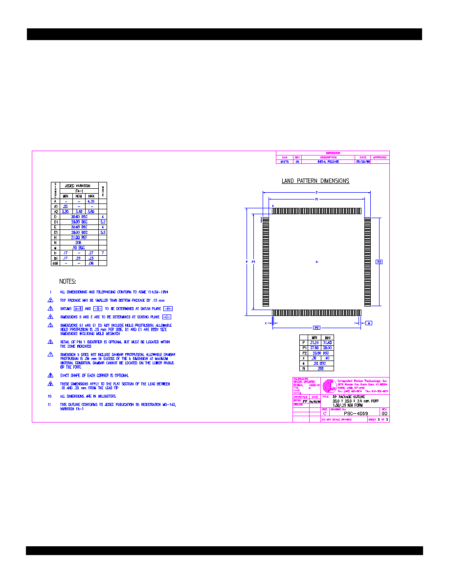
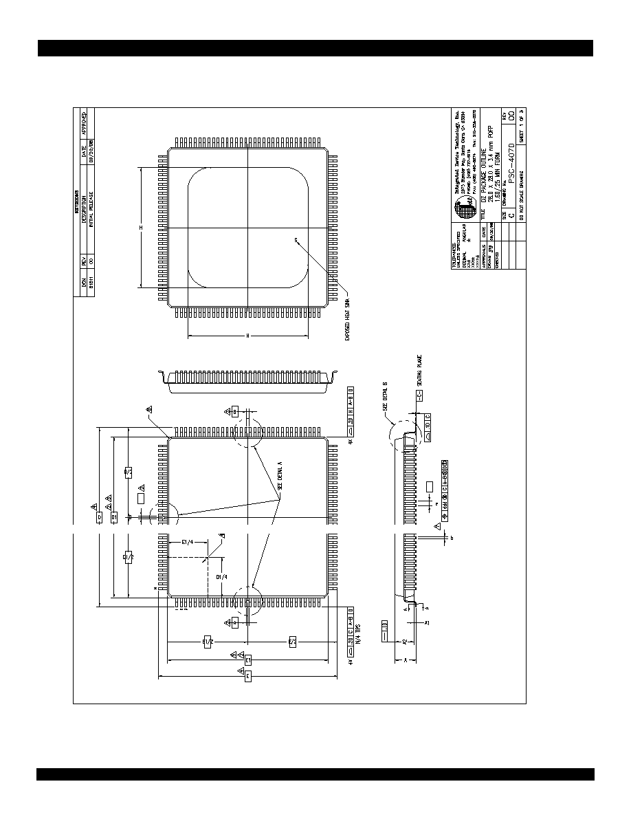
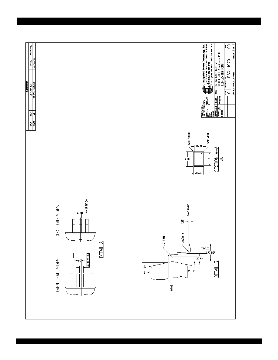
The RC64475 is available in a 208-pin power quad (PQUAD) package.
21 of 25
April 10, 2001
RC64474TM RC64475TM
RC64475 208-pin Package (page 2)
RC64475 208-pin Package (page 2)
RC64475 208-pin Package (page 2)
RC64475 208-pin Package (page 2)
22 of 25
April 10, 2001
RC64474TM RC64475TM
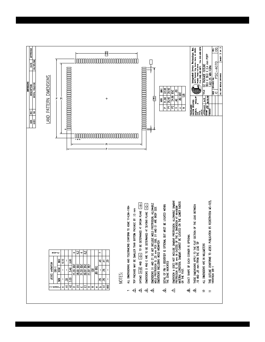
RC64474 128-Pin Package (Page 1 of 3)
RC64474 128-Pin Package (Page 1 of 3)
RC64474 128-Pin Package (Page 1 of 3)
RC64474 128-Pin Package (Page 1 of 3)
23 of 25
April 10, 2001
RC64474TM RC64475TM
RC64474 128-pin Package (page 2 of 3)
RC64474 128-pin Package (page 2 of 3)
RC64474 128-pin Package (page 2 of 3)
RC64474 128-pin Package (page 2 of 3)
24 of 25
April 10, 2001
RC64474TM RC64475TM
RC64474 128-pin Package (Page 3 of 3)
RC64474 128-pin Package (Page 3 of 3)
RC64474 128-pin Package (Page 3 of 3)
RC64474 128-pin Package (Page 3 of 3)
25 of 25
April 10, 2001
RC64474TM RC64475TM
CORPORATE HEADQUARTERS
2975 Stender Way
Santa Clara, CA 95054
for SALES:
800-345-7015 or 408-727-6116
fax: 408-
330-1748
www.idt.com
for Tech Support:
email: rischelp@idt.com
phone: 408-492-8208
The IDT logo is a registered trademark of Integrated Device Technology, Inc.
Ordering Information
Ordering Information
Ordering Information
Ordering Information
Valid combinations
Valid combinations
Valid combinations
Valid combinations
IDT79RC64V474 - 180, 200, 250 DZ
128-pin QFP package, Commercial Temperature
IDT79RC64V475 - 180, 200, 250 DP
208-pin QFP package, Commercial Temperature
IDT79RC64V474 - 180, 200, 250 DZI
128-pin QFP package, Industrial Temperature
IDT79RC64V475 - 180, 200, 250 DPI
208-pin QFP package, Industrial Temperature
IDT79RCXX
YY
XXXX
999
A
A
Operating
Voltage
Device
Type
Speed
Package
Temp range/
Process
V
474
180
200
DZ
Blank
Commercial Temperature
(0∞C to +85∞C Case)
128-pin QFP
180 MHz PClk
200 MHz PClk
3.3V +/-5%
Embedded Processor
Industrial Temperature
(-40∞C to +85∞C Case)
Product
Type
79RC64
64-bit Embedded
Microprocessor
208-pin QFP
DP
250
250 MHz PClk
475
I