COMMERCIAL TEMPERATURE RANGE
MARCH 1996
©1996 Integrated Device Technology, Inc.
DSC-2905/5
IDT79R3041
TM
INTEGRATED RISController
TM
FOR
LOW-COST SYSTEMS
IDT79R3041
IDT79RV3041
FEATURES:
∑ Instruction set compatible with IDT79R3000A
and RISController Family MIPS RISC CPUs
∑ High level of integration minimizes system cost
-- RISC CPU
-- Multiply/divide unit
-- Instruction Cache
-- Data Cache
-- Programmable bus interface
-- Programmable port width support
∑ On-chip instruction and data caches
-- 2KB of Instruction Cache
-- 512B of Data Cache
∑ Flexible bus interface allows simple, low-cost designs
-- Superset pin-compatible with RISController
-- Adds programmable port width interface
(8-, 16-, and 32-bit memory sub-regions)
-- Adds programmable bus interface timing support
(Extended address hold, Bus turn around time,
Read/write masks)
∑ Double-frequency clock input
∑ 16.67MHz, 20MHz, 25MHz and 33MHz operation
∑ 20MIPS at 25MHz
∑ Low cost 84-pin PLCC packaging
∑ On-chip 4-deep write buffer eliminates memory write stalls
∑ On-chip 4-word read buffer supports burst or simple block
reads
∑ On-chip DMA arbiter
∑ On-chip 24-bit timer
∑ Boot from 8-bit, 16-bit, or 32-bit wide PROMs
∑ Pin- and software-compatible family includes R3041, R3051,
R3052
TM
, and R3081
TM
∑ Complete software support
-- Optimizing compilers
-- Real-time operating systems
-- Monitors/debuggers
-- Floating Point emulation software
-- Page Description Languages
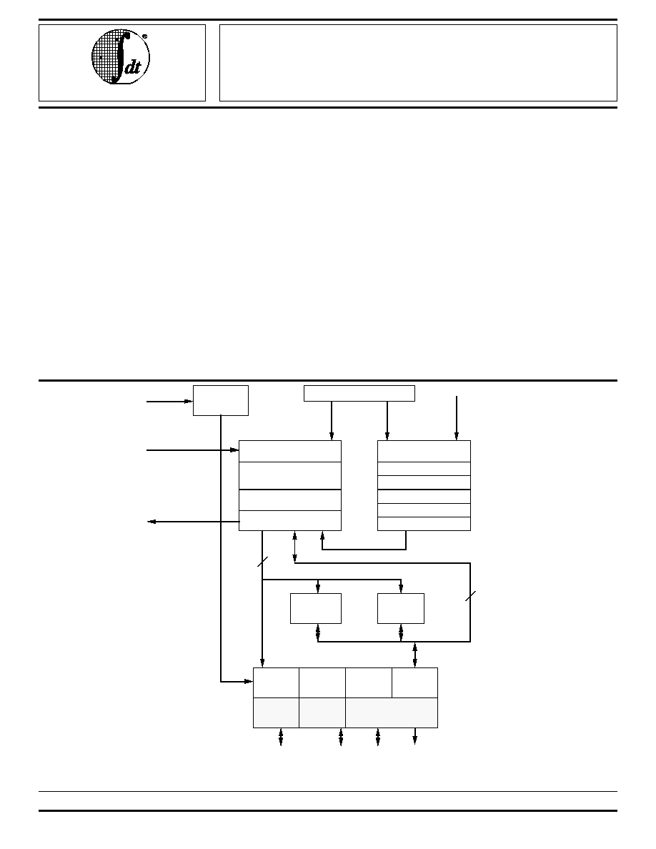
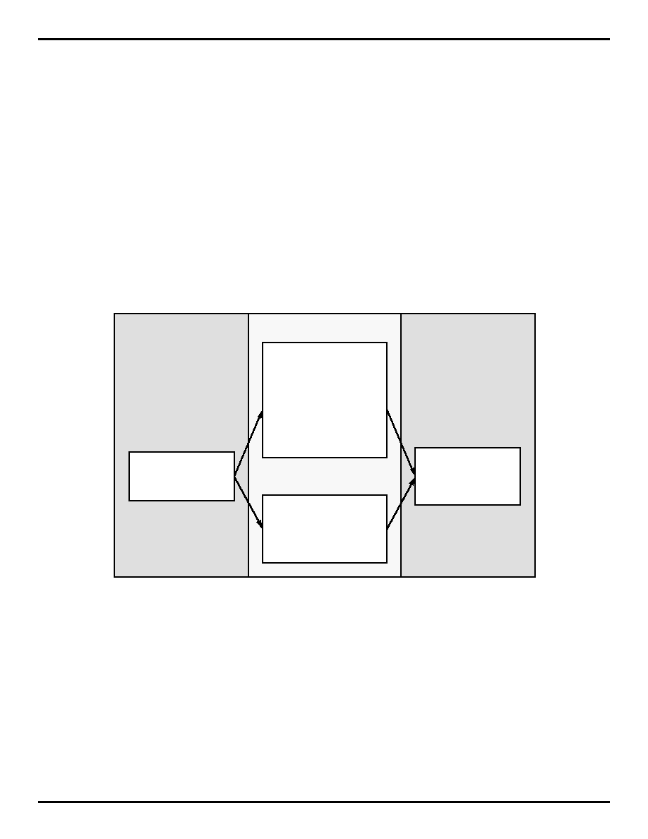
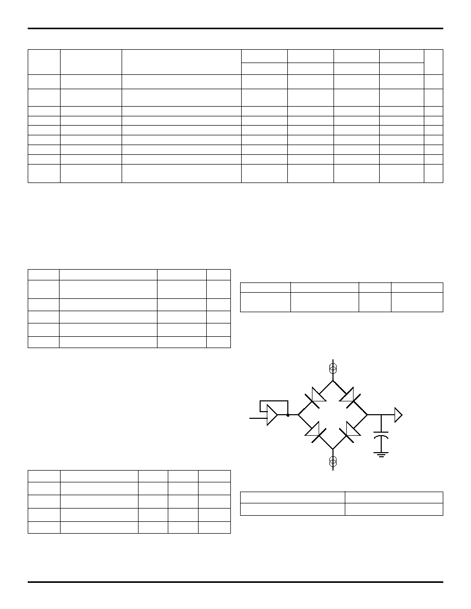
Figure 1. R3041 Block Diagram
Clock
Generator
Unit
Master Pipeline Control
System Control
Coprocessor
Integer
CPU Core
Exception/Control
Registers
Bus Interface
Registers
General Registers
(32 x 32)
ALU
Shifter
Mult/Div Unit
Address Adder
PC Control
Virtual Address
Data
Cache
512B
Instruction
Cache
2kB
Physical Address Bus
BIU
Control
DMA
Arbiter
4-deep
Read
Buffer
4-deep
Write
Buffer
ClkIn
Int(5:3)
,
SInt(2:0)
32
32
SBrCond(3:2)
Data Bus
Address/
Data
DMA
Ctrl
Rd
/
Wr
Ctrl
SysClk
PortSize
Register
Counter
Registers
TC
R3051 Superset
Bus Interface Unit
Data
Unpack
Unit
Data
Pack
Unit
Timing/ Interface
Control
2905 drw 01
1
Integrated Device Technology, Inc.
RISController, R3041, R3051, R3052, R3081, ORION, IDT/sim, and IDT/kit are trademarks, and the IDT logo is a registered trademark of Integrated Device Technology, Inc.
2
IDT79R3041 INTEGRATED RISController FOR LOW COST SYSTEMS
COMMERCIAL TEMPERATURE RANGE
Device
Instruction
Data
Floating
Bus
Name
Cache
Cache
Point
Options
R3051
4kB
2kB
Software Emulation
Mux'ed A/D
R3052
8kB
2kB
Software Emulation
Mux'ed A/D
R3071
16kB
4kB
On-chip Hardware
1/2 frequency bus option
R3081
or 8kB
or 8kB
R3041
2kB
512B
Software Emulation
8-, 16-, and 32-bit port width support
Programmable timing support
2905 tbl 01
INTRODUCTION
The IDT RISController family is a series of high-perfor-
mance 32-bit microprocessors featuring a high-level of inte-
gration, and targeted to high-performance but cost sensitive
embedded processing applications. The RISController family
is designed to bring the high-performance inherent in the
MIPS RISC architecture into low-cost, simplified, power sen-
sitive applications.
Thus, functional units have been integrated onto the CPU
core in order to reduce the total system cost, rather than to
increase the inherent performance of the integer engine.
Nevertheless, the RISController family is able to offer 35MIPS
of integer performance at 40MHz without requiring external
SRAM or caches.
Further, the RISController family brings dramatic power
reduction to these embedded applications, allowing the use of
low-cost packaging. Thus, the RISController family allows
customer applications to bring maximum performance at
minimum cost.
The R3041 extends the range of price/performance achiev-
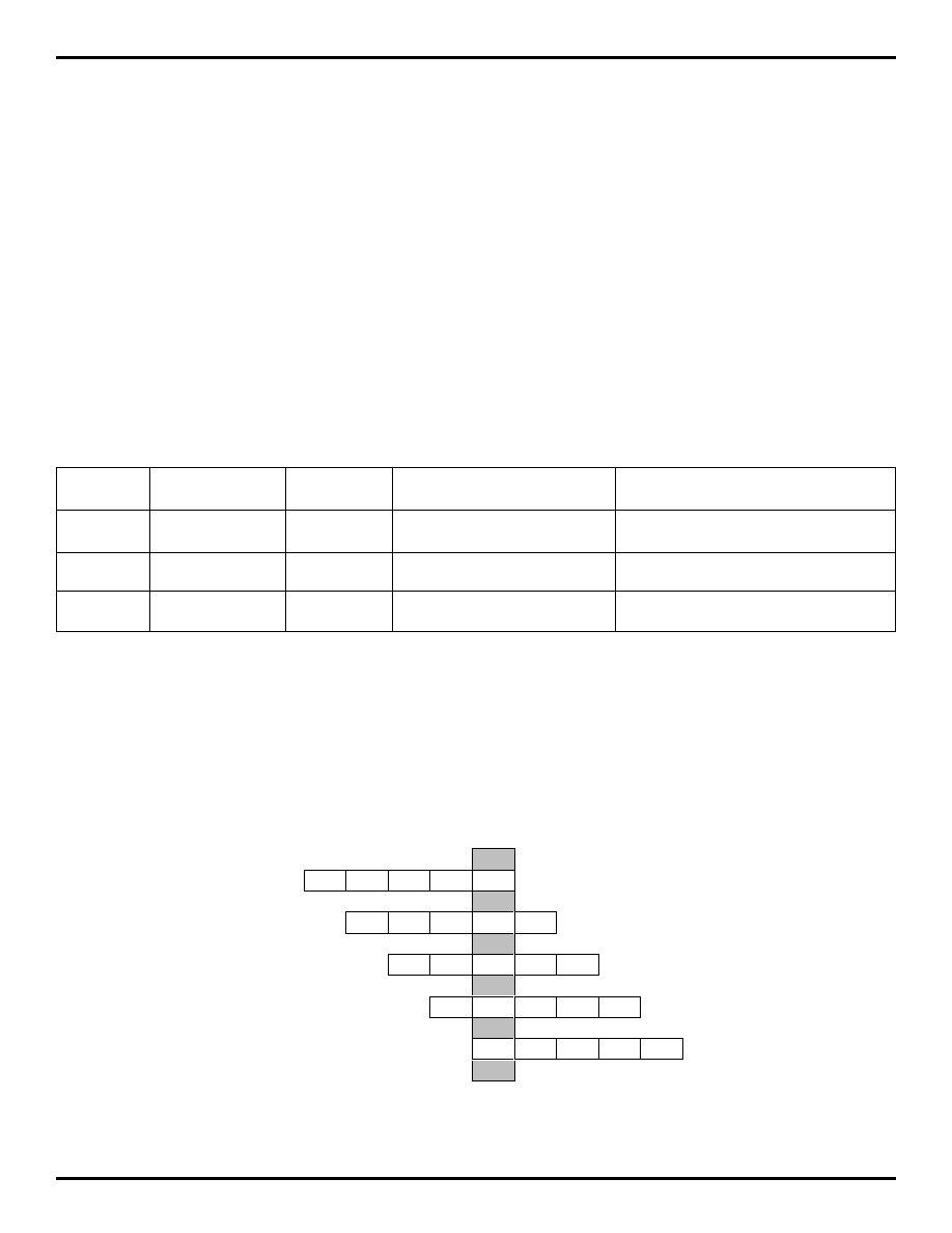
Table 1. Pin-Compatible RISController Family
Figure 2. RISController Family 5-Stage Pipeline
CPU Core
The CPU core is a full 32-bit RISC integer execution
engine, capable of sustaining close to a single cycle execution
rate. The CPU core contains a five stage pipeline, and 32
orthogonal 32-bit registers. The RISController family imple-
ments the MIPS-I Instruction Set Architecture (ISA). In fact,
the execution engine of the R3041 is the same as the
execution engine of the R3000A. Thus, the R3041 is binary
compatible with those CPU engines, as well as compatible
with other members of the RISController family.
able with the RISController family, by dramatically lowering
the cost of using the MIPS architecture. The R3041 is de-
signed to achieve minimal system and components cost, yet
maintain the high-performance inherent in the MIPS architec-
ture. The R3041 also maintains pin and software compatibility
with the RISController and R3081.
The RISController family offers a variety of price/perfor-
mance features in a pin-compatible, software compatible
family. Table 1 provides an overview of the current members
of the RISController family. Note that the R3051, R3052, and
R3081 are also available in pin-compatible versions that
include a full-function memory management unit, including
64-entry TLB. The R3051/2 and R3081 are described in
separate manuals and data sheets.
Figure 1 shows a block level representation of the func-
tional units within the R3041. The R3041 can be viewed as the
embodiment of a discrete solution built around the R3000A.
By integrating this functionality on a single chip, dramatic cost
and power reductions are achieved.
An overview of these blocks is presented here, followed
with detailed information on each block.
IF
Current
CPU
Cycle
I#1
ALU
RD
MEM
WB
IF
I#2
ALU
RD
MEM
WB
IF
I#3
ALU
RD
MEM
WB
IF
I#4
ALU
RD
MEM
WB
IF
I#5
ALU
RD
MEM
WB
2905 drw 02
The execution engine of the RISController family uses a
five-stage pipeline to achieve close to single cycle execution.
A new instruction can be started in every clock cycle; the
execution engine actually processes five instructions concur-
rently (in various pipeline stages). The five parts of the pipeline
are the Instruction Fetch, Read register, ALU execution,
Memory, and Write Back stages. Figure 2 shows the
concurrency achieved by the RISController family pipeline.
3
IDT79R3041 INTEGRATED RISController FOR LOW COST SYSTEMS
COMMERCIAL TEMPERATURE RANGE
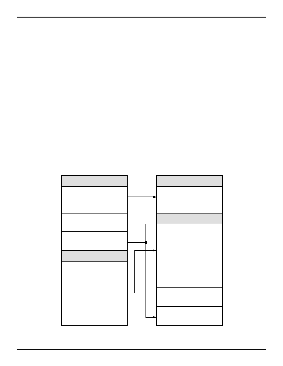
System Control Co-Processor
The R3041 also integrates on-chip a System Control Co-
processor, CP0. CP0 manages the exception handling capa-
bility of the R3041, the virtual to physical address mapping of
the R3041, and the programmable bus interface capabilities
of the R3041. These topics are discussed in subsequent
sections.
The R3041 does not include the optional TLB found in other
members of the RISController family, but instead performs the
same virtual to physical address mapping of the base version
of the RISController family. These devices still support
distinct kernel and user mode operation, but do not require
page management software or an on-chip TLB, leading to a
simpler software model and a lower-cost processor.
The memory mapping used by these devices is illustrated
in Figure 3. Note that the reserved address spaces shown are
for compatibility with future family members; in the current
family members, references to these addresses are trans-
lated in the same fashion as their respective segments, with
no traps or exceptions taken.
When using the base versions of the architecture, the
system designer can implement a distinction between the
user tasks and the kernel tasks, without having to execute
page management software. This distinction can take the
form of physical memory protection, accomplished by ad-
dress decoding, or in other system specific forms. In systems
which do not wish to implement memory protection, and wish
to have the kernel and user tasks operate out of a single
unified memory space, upper address lines can be ignored by
the address decoder, and thus all references will be seen in
the lower gigabyte of the physical address space.
The R3041 adds additional resources into the on-chip CP0.
These resources are detailed in the R3041 User's Manual.
They allow kernel software to directly control activity of the
processor internal resources and bus interface, and include:
∑ Cache Configuration Register: This register controls the
data cache block size and miss refill algorithm.
∑ Bus Control Register: This register controls the behavior
of the various bus interface signals.
∑ Count and Compare Registers: Together, these two
registers implement a programmable 24-bit timer, which
can be used for DRAM refresh or as a general purpose
timer.
∑ Port Size Control Register: This register allows the kernel
to indicate the port width of reads and writes to various sub-
regions of the physical address space. Thus, the R3041 can
interface directly with 8-, 16-, and 32-bit memory ports,
including a mix of sizes, for both instruction and data
references, without requiring additional external logic.
Figure 3. Virtual to Physical Mapping of Base Architecture Versions
VIRTUAL
PHYSICAL
2905 drw 03
Kernel Cached
(kseg2)
Kernel Uncached
(kseg1)
Kernel Cached
(kseg0)
Kernel/User
Cached
(kuseg)
Kernel Cached
Tasks
1023 MB
Kernel/User
Cached
Tasks
2047 MB
Inaccessible
512 MB
Kernel Boot
and I/O
512 MB
0xfff00000
0xc0000000
0xa0000000
0x00000000
0xffffffff
0x80000000
0x7fffffff
0x7ff00000
0x7fefffff
0x9fffffff
0xbfffffff
0xffefffff
User Reserved
1MB
Kernel Reserved
1MB
0xfff00000
0xc0000000
0xbff00000
0x00000000
0xffffffff
0x40000000
0x3fffffff
0x20000000
0x1fffffff
0xbfefffff
0xbfffffff
0xffefffff
Kernel Reserved
1MB
User Reserved
1MB

4
IDT79R3041 INTEGRATED RISController FOR LOW COST SYSTEMS
COMMERCIAL TEMPERATURE RANGE
Clock Generation Unit
The R3041 is driven from a single 2x frequency input clock,
capable of operating in a range of 40%-60% duty cycle. On-
chip, the clock generator unit is responsible for managing the
interaction of the CPU core, caches, and bus interface. The
clock generator unit replaces the external delay line required
in R3000A based applications.
Instruction Cache
The R3041 integrates 2kB of on-chip Instruction Cache,
organized with a line size of 16 bytes (four 32-bit entries) a nd
is direct mapped. This relatively large cache substantially
contributes to the performance inherent in the R3041, and
allows systems based on the R3041 to achieve high-perfor-
mance even from low-cost memory systems. The cache is
implemented as a direct mapped cache, and is capable of
caching instructions from anywhere within the 4GB physical
address space. The cache is implemented using physical
addresses and physical tags (rather than virtual addresses or
tags), and thus does not require flushing on context switch.
Data Cache
The R3041 incorporates an on-chip data cache of 512B,
organized as a line size of 4 bytes (one word) and is direct
mapped. This relatively large data cache contributes substan-
tially to the performance inherent in the RISController family.
As with the instruction cache, the data cache is implemented
as a direct mapped physical address cache. The cache is
capable of mapping any word within the 4GB physical address
space.
The data cache is implemented as a write through cache,
to insure that main memory is always consistent with the
internal cache. In order to minimize processor stalls due to
data write operations, the bus interface unit incorporates a 4-
deep write buffer which captures address and data at the
processor execution rate, allowing it to be retired to main
memory at a much slower rate without impacting system
performance.
Bus Interface Unit
The RISController family uses its large internal caches to
provide the majority of the bandwidth requirements of the
execution engine, and thus can utilize a simple bus interface
connected to slow memory devices.
The RISController family bus interface utilizes a 32-bit
address and data bus multiplexed onto a single set of pins.
The bus interface unit also provides an ALE (Address Latch
Enable) output signal to de-multiplex the A/D bus, and simple
handshake signals to process CPU read and write requests.
In addition to the read and write interface, the R3041 incorpo-
rates a DMA arbiter, to allow an external master to control the
external bus.
The R3041 augments the basic RISController bus interface
capability by adding the ability to directly interface with varying
memory port widths, for instructions or data. For example, the
R3041 can be used in a system with an 8-bit boot PROM, 16-
bit font/program cartridges, and 32-bit main memory, trans-
parently to software, and without requiring external data
packing, rotation, and unpacking.
In addition, the R3041 incorporates the ability to change
some of the interface timing of the bus. These features can be
used to eliminate external data buffers and take advantage of
lower speed and lower cost interface components.
One of the bus interface options is the Extended Address
Hold mode which adds 1/2 clock of extra address hold time
from ALE falling. This allows easier interfacing to FPGAs and
ASICs.
The R3041 incorporates a 4-deep write buffer to decouple
the speed of the execution engine from the speed of the
memory system. The write buffers capture and FIFO proces-
sor address and data information in store operations, and
present it to the bus interface as write transactions at the rate
the memory system can accommodate. During main memory
writes, the R3041 can break a large datum (e.g. 32-bit word)
into a series of smaller transactions (e.g. bytes), according to
the width of the memory port being written. This operation is
transparent to the software which initiated the store, insuring
that the same software can run in true 32-bit memory systems.
The RISController family read interface performs both
single word reads and quad word reads. Single word reads
work with a simple handshake, and quad word reads can
either utilize the simple handshake (in lower performance,
simple systems) or utilize a tighter timing mode when the
memory system can burst data at the processor clock rate.
Thus, the system designer can choose to use page or static
column mode DRAMs (and possibly use interleaving, if de-
sired, in high-performance systems), or even to use simpler
SRAM techniques to reduce complexity.
In order to accommodate slower quad word reads, the
RISController family incorporates a 4-deep read buffer FIFO,
so that the external interface can queue up data within the
processor before releasing it to perform a burst fill of the
internal caches.
In addition, the R3041 can perform on-chip data packing
when performing large datum reads (e.g., quad words) from
narrower memory systems (e.g., 16-bits). Once again, this
operation is transparent to the actual software, simplifying
migration of software to higher performance (true 32-bit)
systems, and simplifying field upgrades to wider memory.
Since this capability works for either instruction or data reads,
using 8-, 16-, or 32-bit boot PROMs is easily supported by the
5
IDT79R3041 INTEGRATED RISController FOR LOW COST SYSTEMS
COMMERCIAL TEMPERATURE RANGE
R3041.
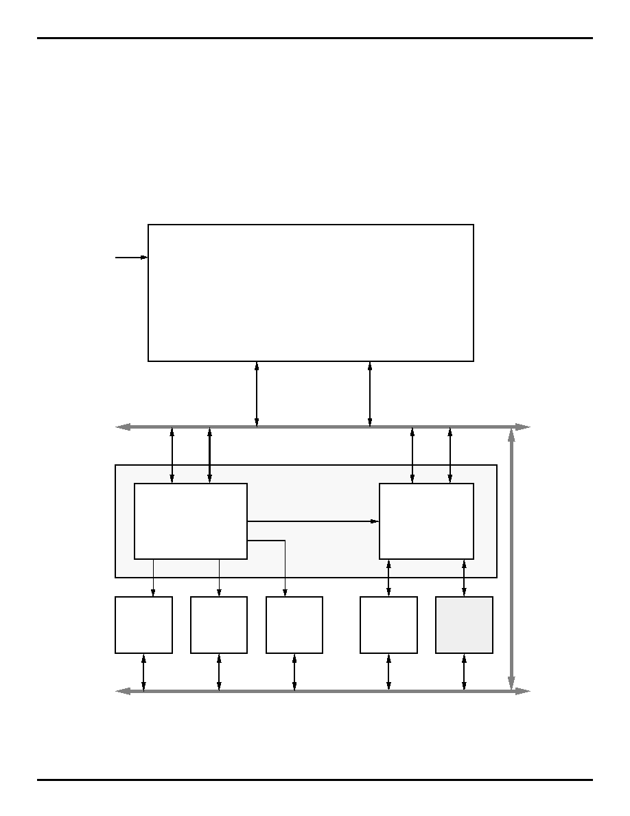
SYSTEM USAGE
The IDT RISController family is specifically designed to
easily connect to low-cost memory systems. Typical low-cost
memory systems use inexpensive EPROMs, DRAMs, and
application specific peripherals.
Figure 4 shows some of the flexibility inherent in the R3041.
In this example system, which is typical of a laser printer, a 32-
bit PROM interface is used due to the size of the PDL
interpreter. An embedded system can optionally use an 8-bit
Figure 4. Typical R3041-Based Application
boot PROM instead. A 16-bit font/program cartridge interface
is provided for add-in cards. A 16-bit DRAM interface is used
for a low-cost page frame buffer. In this system example, a
field or manufacturing upgrade to a 32-bit page frame buffer
is supported by the boot software and DRAM controller.
Embedded systems may optionally substitute SRAMs for the
DRAMs. Finally various 8/16/32-bit I/O ports such as RS-232/
422, SCSI, and LAN as well as the laser printer engine
interface are supported. Such a system features a very low
entry price, with a range of field upgrade options including the
ability to upgrade to a more powerful member of the
RISController family.
ClkIn
IDT R3041
RISController
Address/
Data
Control
EPROM and
I/O Controller
DRAM
Controller
16-bit
DRAM
16-bit
Add-on
DRAM
32-bit
EPROM
16-bit
Font
Cartridge
I/O
R3051
Local Bus
2905 drw 04
6
IDT79R3041 INTEGRATED RISController FOR LOW COST SYSTEMS
COMMERCIAL TEMPERATURE RANGE
DEVELOPMENT SUPPORT
The IDT RISController family is supported by a rich set of
development tools, ranging from system simulation tools
through PROM monitor and debug support, applications soft-
ware and utility libraries, logic analysis tools, and sub-system
modules.
Figure 5 is an overview of the system development process
typically used when developing R3041 applications. The
RISController family is supported in all phases of project
development. These tools allow timely, parallel development
of hardware and software for RISController family based
applications, and include tools such as:
∑ Optimizing compilers from MIPS Technology, the acknowl-
edged leader in optimizing compiler technology.
∑ Cross development tools, available in a variety of develop-
ment environments.
∑ The high-performance IDT floating point emulation library
software.
∑ The IDT Evaluation Board, which includes RAM, EPROM,
I/O, and the IDT PROM Monitor.
∑ IDT Laser Printer System boards, which directly drive a low-
cost print engine, and runs Adobe PostScript
TM
Page De-
scription Language
∑ Adobe PostScript Page Description Language running on
the IDT RISController family.
∑ The IDT/sim
TM
PROM Monitor, which implements a full
PROM monitor (diagnostics, remote debug support, peek/
Figure 5. R3041 Development Environment
Cache3041
Benchmarks
Evaluation Board
Laser Printer System
DBG Debugger
PIXIE Profiler
MIPS Compiler Suite
Stand-Alone Libraries
Floating Point Library
Cross Development Tools
Adobe PostScript PDL
MicroSoft TrueImage PDL
PeerlessPage BIOS
IDT/kit
Hardware Models
General CAD Tools
RISC Sub-systems
'341 Evaluation Board
Laser Printer System
Logic Analysis
Diagnostics
IDT/sim PROM Monitor
Remote Debug
Real-Time OS
Software
Hardware
System
Integration
and Verfification
System
Development
Phase
System
Architecture
Evaluation
2905 drw 05

7
IDT79R3041 INTEGRATED RISController FOR LOW COST SYSTEMS
COMMERCIAL TEMPERATURE RANGE
poke, etc.).
∑ IDT/kit
TM
(Kernel Integration Toolkit), providing library sup-
port and a frame work for the system run time environment.
PERFORMANCE OVERVIEW
The RISController family achieves a very high-level of
performance. This performance is based on:
∑ An efficient execution engine: The CPU performs ALU
operations and store operations in a single cycle, and has
an effective load time of 1.3 cycles, and branch execution
rate of 1.5 cycles (based on the ability of the compilers to
avoid software interlocks). Thus, the R3041 achieves 20
MIPS performance at 25MHz when operating out of cache.
∑ Large on-chip caches: The RISController family contains
caches which are substantially larger than those on the
majority of embedded microprocessors. These large caches
minimize the number of bus transactions required, and
allow the RISController family to achieve actual sustained
performance very close to its peak execution rate, even with
low-cost memory systems.
∑ Autonomous multiply and divide operations: The
RISController family features an on-chip integer multiplier/
divide unit which is separate from the other ALU. This allows
the R3041 to perform multiply or divide operations in parallel
with other integer operations, using a single multiply or
divide instruction rather than using "step" operations.
∑ Integrated write buffer: The R3041 features a four deep
write buffer, which captures store target addresses and data
at the processor execution rate and retires it to main
memory at the slower main memory access rate. Use of on-
chip write buffers eliminates the need for the processor to
stall when performing store operations.
∑ Burst read support: The R3041 enables the system
designer to utilize page mode, static column, or nibble mode
RAMs when performing read operations to minimize the
main memory read penalty and increase the effective cache
hit rates.
The performance differences among the various
RISController family members depends on the application
software and the design of the memory system. Different
family members feature different cache sizes, and the R3081
features a hardware floating point accelerator. Since all these
devices can be used in a pin and software compatible fashion,
the system designer has maximum freedom in trading be-
tween performance and cost. The memory simulation tools
(e.g. Cache3041) allows the system designers to analyze and
understand the performance differences among these de-
vices in their application.
SELECTABLE FEATURES
The RISController family uses two methods to allow the
system designer to configure bus interface operation options.
The first set of options are established via the Reset
Configuration Mode inputs, sampled during the device reset.
After reset, the Reset Mode inputs become regular input or
output signals.
The second set of configuration options are contained in
the System Control Co-Processor registers. These Co-pro-
cessor registers configuration options are typically initialized
with the boot PROM and can also be changed dynamically by
the kernel software.
Selectable features include:
∑ Big Endian vs. Little Endian operation: The part can be
configured to operate with either byte ordering convention,
and in fact may also be dynamically switched between the
two conventions. This facilitates the porting of applications
from other processor architectures, and also permits inter-
communication between various types of processors and
databases.
∑ Data Cache Refill of one or four words: The memory
system must be capable of performing 4 word transfers to
satisfy instruction cache misses and 1 word transfers to
satisfy uncached references. The data cache refill size
option allows the system designers to choose between one
and four word refill on data cache misses, depending on the
performance each option brings to their application.
∑ Bus Turn Around speed: The R3041 allows the kernel to
increase the amount of time between bus transactions
when changes in direction of the A/D bus occur (e.g., at the
end of reads followed by writes). This allows transceivers
and buffers to be eliminated from the system.
∑ Extended Address Hold Time: The R3041 allows the
system designer to increase the amount of hold time avail-
able for address latching, thus allowing slower speed (low
cost) address latches, FPGAs and ASICs to be used.
∑ Programmable control signals: The R3041 allows the
system designer to optimally configure various memory
control signals to be active on reads only, writes only, or on
both reads and writes. This allows the simplification of
external logic, thus reducing system cost.
8
IDT79R3041 INTEGRATED RISController FOR LOW COST SYSTEMS
COMMERCIAL TEMPERATURE RANGE
∑ Programmable memory Port Widths: The R3041 allows
the kernel to partition the physical memory space into
various sub-regions, and to individually indicate the port
width of these sub-regions. Thus, the bus interface unit can
perform data packing and unpacking when communicating
with narrow memory sub-regions. For example, these fea-
tures, can be used to allow the R3041 to interface with
narrow 8-bit boot PROMs, or to implement 16-bit only
memory systems.
THERMAL CONSIDERATIONS
The RISController family utilizes special packaging tech-
niques to improve the thermal properties of high-speed pro-
cessors. Thus, all versions of the RISController family are
packaged in cavity down packaging.
The lowest cost members of the family use a standard
cavity down, injection molded PLCC package (the "J" pack-
age). This package is used for all speeds of the R3041 family.
Higher speed and higher performance members of the
RISController family utilize more advanced packaging tech-
niques to dissipate power while remaining both low-cost and
pin- and socket- compatible with the PLCC package. Thus,
these members of the RISController family are available in the
MQUAD package (the "MJ" package), which is an all alumi-
num package with the die attached to a normal copper lead-
frame mounted to the aluminum casing. The MQUAD pack-
age is pin and form compatible with the PLCC package. Thus,
designers can choose to utilize this package without changing
their PCB.
The members of the RISController family are guaranteed in
a case temperature range of 0
∞
C to +85
∞
C. The type of
package, speed (power) of the device, and airflow conditions,
affect the equivalent ambient conditions which meet this
specification.
The equivalent allowable ambient temperature, T
A
, can be
calculated using the thermal resistance from case to ambient
(ÿ
CA
) of the given package. The following equation relates
ambient and case temperature:
T
A
= T
C
- P * ÿ
CA
where P is the maximum power consumption at hot tempera-
ture, calculated by using the maximum Icc specification for the
device.
Typical values for ÿ
CA
at various airflows are shown in
Table 2 for the PLCC package.
NOTES ON SYSTEM DESIGN
The R3041 has been designed to simplify the task of high-
speed system design. Thus, set-up and hold-time require-
ments have been kept to a minimum, allowing a wide variety
of system interface strategies.
To minimize these AC parameters, the R3041 employs
feedback from its SysClk output to the internal bus interface
unit. This allows the R3041 to reference input signals to the
reference clock seen by the external system. The SysClk
output is designed to provide relatively large AC drive to
minimize skew due to slow rise or fall times. A typical part will
have less than 2ns rise or fall (10% to 90% signal times) when
driving the test load.
Therefore, the system designer should use care when
designing for direct SysClk use. Total loading (due to devices
connected on the signal net and the routing of the net itself)
should be minimized to ensure the SysClk output has a
smooth and rapid transition. Long rise and/or fall times may
cause a degradation in the speed capability of an individual
device.
Similarly, the R3041 employs feedback on its ALE output to
ensure adequate address hold time to ALE. The system
designer should be careful when designing the ALE net to
minimize total loading and to minimize skew between ALE and
the A/D bus, which will ensure adequate address access latch
time.
IDT's field and factory applications groups can provide the
system designer with assistance for these and other design
issues.
Airflow (ft/min)
ÿCA
0
200
400
600
800
1000
"J" Package
29
26
21
18
16
15
TQFP
55
40
35
33
31
30
2905 tbl 02
Table 2. Thermal Resistance (ÿ
CA
) at Various Airflows

9
IDT79R3041 INTEGRATED RISController FOR LOW COST SYSTEMS
COMMERCIAL TEMPERATURE RANGE
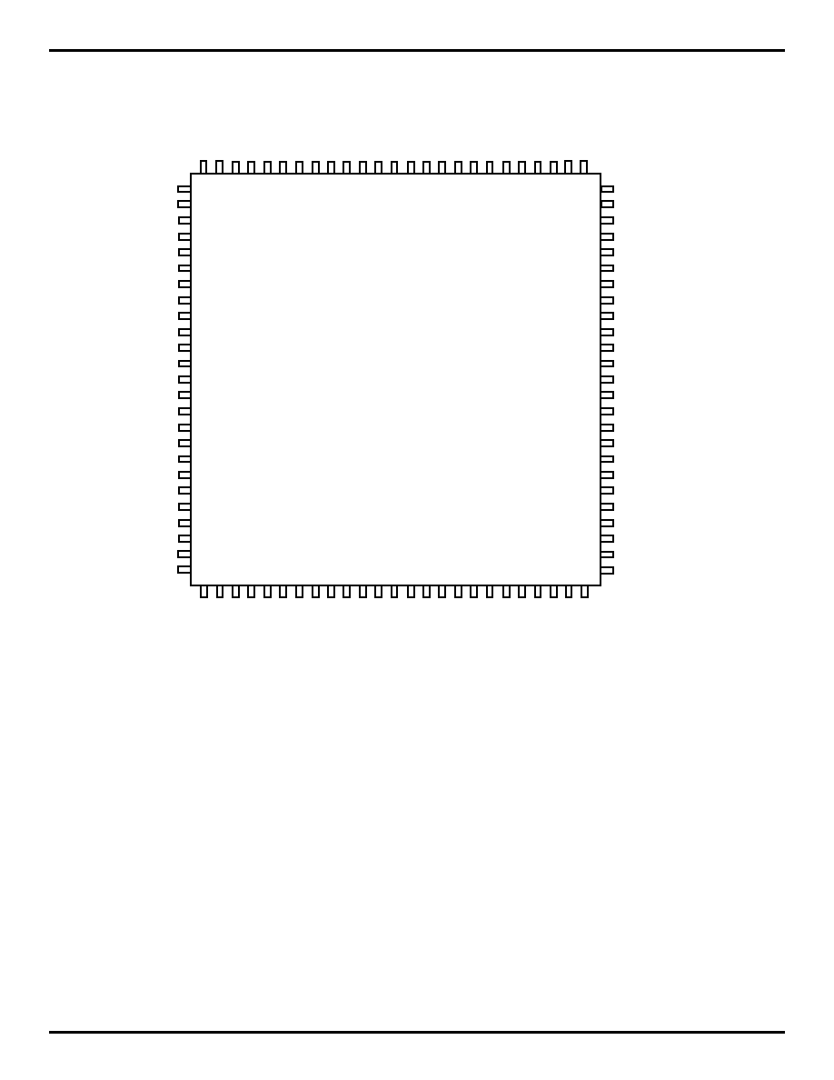
PIN CONFIGURATIONS
IDT R3041/RV3041
84-Pin PLCC/
Top View
(Cavity Down)
V
SS
V
CC
A/D(14)
A/D(13)
A/D(12)
A/D(11)
A/D(10)
A/D(9)
V
CC
V
SS
A/D(8)
A/D(7)
A/D(6)
A/D(5)
A/D(4)
A/D(3)
V
SS
V
CC
A/D(2)
A/D(1)
A/D(0)
Burst/WrNear
Addr(3)
Addr(2)
Diag
Last
ALE
Rd
Wr
DataEn
V
CC
V
SS
SysClk
BusGnt
Reset
BusError
Ack
RdCEn
BusReq
MemStrobe
V
SS
V
CC
ClkIn
TriState
BE16(1)
BE16(0)
Addr(1)
Addr(0)
Int(5)
V
SS
V
CC
Int(4)
Int(3)
SInt(2)
SInt(1)
SInt(0)
TC
V
SS
V
CC
A/D(15)
A/D(16)
A/D(17)
A/D(18)
A/D(19)
A/D(20)
A/D(21)
A/D(22)
A/D(23)
A/D(24)
A/D(25)
A/D(26)
V
CC
V
SS
A/D(27)
A/D(28)
A/D(29)
A/D(30)
A/D(31)
1
84
12
75
33
54
SBrCond(3)/
IOStrobe
SBrCond(2)/
ExtDataEn
13
14
2
3
4
5
6
7
8
9
10
11
83
82
81 80
79 78 77
76
15
16
17
18
19
20
21
22
23
24
25
26
27
28
29
30
31
32
34
35 36 37
38 39
40
41 42 43 44 45
46 47
48 49
50 51 52
53
55
56
57
58
59
60
61
62
63
64
65
66
67
68
69
70
71
72
73
74
V
CC
V
SS
V
CC
V
SS
2905 drw 06
10
IDT79R3041 INTEGRATED RISController FOR LOW COST SYSTEMS
COMMERCIAL TEMPERATURE RANGE
PIN CONFIGURATIONS
2905 drw 06
SBrCond(2)/
ExtDataEn
SBrCond(3)/
IOStrobe
1
12
13
14
2
3
4
5
6
7
8
9
10
11
15
16
17
18
19
20
21
22
23
24
25
V
SS
V
CC
ClkIn
TriState
BE16(1)
BE16(0)
Addr(1)
Addr(0)
Int(5)
V
SS
V
CC
Int(4)
Int(3)
SInt(2)
SInt(1)
SInt(0)
TC
V
SS
V
CC
V
SS
V
CC
A/D(14)
A/D(13)
A/D(12)
A/D(11)
A/D(10)
A/D(9)
V
CC
V
SS
A/D(8)
A/D(7)
A/D(6)
A/D(5)
A/D(4)
A/D(3)
V
SS
V
CC
A/D(2)
A/D(1)
A/D(0)
26
27
28
29
30
31
32
33
34
35
36
37
38
39
40
41
42
43
44
45
46
47
48
49
50
54
52 53
55 56 57 58 59 60
51
61 62 63 64 65 66 67 68 69 70 71 72 73 74 75
76
77
78
79
80
81
82
83
84
85
86
87
88
89
90
91
92
93
94
95
96
97
98
99
100
NC
NC
NC
NC
NC
NC
NC
NC
A/D(15)
A/D(16)
A/D(17)
A/D(18)
A/D(19)
A/D(20)
A/D(21)
A/D(22)
A/D(23)
A/D(24)
A/D(25)
A/D(26)
A/D(27)
A/D(28)
A/D(29)
A/D(30)
A/D(31)
V
CC
V
SS
V
CC
V
SS
NC
NC
NC
NC
Burst/WrNear
Addr(3)
Addr(2)
Diag
Last
ALE
Rd Wr DataEn
V
CC
V
SS
SysClk BusGnt Reset BusError Ack RdCEn BusReq MemStrobe
V
CC
V
SS
NC
NC
NC
NC
IDT R3041/RV3041
100-Pin
TQFP
(Cavity Up)
Top View

11
IDT79R3041 INTEGRATED RISController FOR LOW COST SYSTEMS
COMMERCIAL TEMPERATURE RANGE
PIN DESCRIPTION
PIN NAME
I/O
DESCRIPTION
A/D(31:0)
I/O
Address/Data: A 32-bit time multiplexed bus which indicates the desired address for a bus transaction
in one phase, and which is used to transmit data between the CPU and external memory resources during
the rest of the transfer.
Bus transactions on this bus are logically separated into two phases: during the first phase, information
about the transfer is presented to the memory system to be captured using the ALE output. This
information consists of:
Address(31:4):
The high-order address for the transfer is presented on A/D(31:4).
BE(3:0):
These strobes indicate which bytes of the 32-bit bus will be involved in
the transfer, and are presented on A/D(3:0).
BE(3
) indicates that
A/D(31:24) will be used, and
BE(0)
corresponds to A/D(7:0). These
strobes are only valid for accesses to 32-bit wide memory ports. Note
that
BE(3:0)
can be held in-active during reads by setting the appropriate
bit of CP0; thus when latched, these signals can be directly used as Write
Enable strobes.
During the second phase, these signals are the data bus for the transaction.
Data(31:0):
During write cycles, the bus contains the data to be stored and is driven
from the internal write buffer.
On read cycles, the bus receives the data from the external resource, in
either a single data transaction or in a burst of four words, and places it
into the on-chip read buffer.
The byte lanes used during the transfer are a function of the datum size,
the memory port width, and the system byte-ordering.
Addr(3:0)
O
Low Address (3:0) A 4-bit bus which indicates which word/halfword/byte is currently expected by the
processor. For 32-bit port widths, only Addr(3:2) is valid during the transfer; for 16-bit port widths, only
Addr(3:1) are valid; for 8-bit port widths, all of Addr(3:0) are valid. These address lines always contain
the address of the current datum to be transferred. In writes and single datum reads, the addresses initially
output the specific target address, and will increment if the size of the datum is wider than the target
memory port. For quad word reads, these outputs function as a counter starting at '0000', and
incrementing according to the width of the memory port.
I
(1)
During
Reset
, the Addr(3:0) pins act as Reset Configuration Mode bit inputs for the
BootProm16
,
BootProm8
, ReservedHigh, and
ExtAddrHold
options.
The R3041 Addr(1:0) output pins are designated as the unconnected Rsvd(1:0) pins in the R3051 and
R3081.
Diag
O
Diagnostic Pin. This output indicates whether the current bus read transaction is due to an on-
chip cache miss and whether the read is an instruction or data. It is time multiplexed as described below:
Cached/
Uncached
:
During the phase in which the A/D bus presents address information, this
pin is an active high output which indicates whether or not the current
read is a result of a cache miss. The value of this pin at this time other
than in read cycles is undefined.
I/
D:
A high at this time indicates an instruction reference, and a low indicates
a data reference. The value of this pin at this time other than in read
cycles is undefined.
The R3041 Diag output pin is designated as the Diag(1) output pin in the R3051 and R3081.
ALE
O
Address Latch Enable: Used to indicate that the A/D bus contains valid address information for
the bus transaction. This signal is used by external logic to capture the address for the transfer, typically
by using transparent latches.
DataEn
O
Data Enable: This signal indicates that the A/D bus is no longer being driven by the processor
during read cycles, and thus the external memory system may enable the drivers of the memory
system onto this bus without having a bus conflict occur. During write cycles, or when no bus
trans-
action is occurring, this signal is negated, thus disabling the external memory drivers.
2905 tbl 03
NOTE:
1. Reset Configuration Mode bit input when
Reset
is asserted, normal signal
function when
Reset
is de-asserted.

12
IDT79R3041 INTEGRATED RISController FOR LOW COST SYSTEMS
COMMERCIAL TEMPERATURE RANGE
PIN DESCRIPTION (Continued):
PIN NAME
I/O
DESCRIPTION
Burst/
O
Burst Transfer/Write Near: On read transactions, the
Burst
signal indicates that the current bus read
WrNear
is requesting a block of four contiguous words from memory. This signal is asserted only in read cycles
due to cache misses; it is asserted for all I-Cache miss read cycles, and for D-Cache miss read cycles
if the 4-word data block refill option is selected in the CP0 Cache Config Register.
On write transactions, the
WrNear
output tells the external memory system that the bus interface unit
is performing back-to-back write transactions to an address within the same 256 byte page as the prior
write transaction. This signal is useful in memory systems which employ page mode or static column
DRAMs, and allows nearby writes to be retired quickly.
Rd
O
Read: An output which indicates that the current bus transaction is a read.
Wr
O
Write: An output which indicates that the current bus transaction is a write.
Ack
I
Acknowledge: An input which indicates to the device that the memory system has sufficiently
processed the bus transaction. On write transactions, this signal indicates that the CPU may either
progress to the next data item (for mini-burst writes of wide datums to narrow memories), or terminate
the write cycle. On read transactions, this signal indicates that the memory system has sufficiently
processed the read, and that the processor core may begin processing the data from this read transfer.
RdCEn
I
Read Buffer Clock Enable: An input which indicates to the device that the memory system has
placed valid data on the A/D bus, and that the processor may move the data into the on-chip Read
Buffer.
SysClk
O
System Reference Clock: An output from the CPU which reflects the timing of the internal
processor "System" clock. This clock is used to control state transitions in the read buffer, write buffer,
memory controller, and bus interface unit.
BusReq
I
DMA Arbiter Bus Request: An input to the device which requests that the CPU tri-state its bus
interface signals so that they may be driven by an external master. The negation of this input relinquishes
mastership back to the CPU.
BusGnt
O
DMA Arbiter Bus Grant. An output from the CPU used to acknowledge that a
BusReq
has been
detected, and that the bus is relinquished to the external master.
The R3041 adds an additional DMA protocol, under the control of CP0. If the DMA Protocol is enabled,
the R3041 can request that the external master relinquish bus mastership back to the processor by
negating the
BusGnt
output early, and waiting for the
BusReq
input to be negated.
SBrCond(3)/
I/O
Branch Condition Port/IO Strobe: The use of this signal depends on the setting of various bits of the
IOStrobe
CP0 Bus Control register. If BrCond mode is selected, this input is logically connected to CpCond(3),
and can be used by the branch on co-processor condition instructions as an input port. The SBrCond(3)
input has special internal logic to synchronize the input, and thus may be driven by asynchronous
agents.
If this pin is selected to function as
IOStrobe
, it may be asserted as an output on reads, writes, or both,
as programmed into CP0. This strobe asserts in the second clock cycle of a transfer, and thus can be
used to strobe various control signals on the bus interface.
SBrCond(2)/
I/O
Branch Condition Port/Extended Data Enable: The use of this signal depends on the settings in the
ExtDataEn
CP0 Bus Control register. If BrCond mode is selected, this input is logically connected to CpCond(2),
and can be used by the branch on co-processor condition instructions as an input port. The SBrCond(2)
input has special internal logic to synchronize the input, and thus may be driven by asynchronous
agents.
If this pin is selected to function as Extended Data Enable, it may be asserted as an output on reads,
writes, or both, as programmed into CP0. This strobe can be used as an extended data enable strobe,
in that it is held asserted for one-half clock cycle after the negation of
Rd
or
Wr
. This signal may typically
be used as a write enable control line for transceivers, as a write line for I/O, or as an address mux select
for DRAMs.
MemStrobe
O
Memory Strobe: This active low output pulses low for each data read or written, as configured in the
CP0 Bus Control register. Thus, it can be used as a read strobe, write strobe, or both, for SRAM type
memories or for I/O devices.
The R3041
MemStrobe
output pin is designated as the BrCond(0) input pin in the R3051 and R3081.
2905 tbl 04

13
IDT79R3041 INTEGRATED RISController FOR LOW COST SYSTEMS
COMMERCIAL TEMPERATURE RANGE
PIN NAME
I/O
DESCRIPTION
BE16(1:0)
O
Byte Enable Strobes for 16-bit Memory Port: These active low outputs are the byte lane strobes for
accesses to 16-bit wide memory ports; they are not necessarily valid for 8- or 32-bit wide ports. If
BE16(1
)
is asserted, then the most significant byte (either D(31:24) or D(15:8), depending on system endianness)
is going to be used in this transfer. If
BE16(0)
is asserted, the least significant byte (D(23:16) or D(7:0))
will be used.
BE16(1:0)
can be held inactive (masked) during read transfers, according to the programming of the CP0
Bus Control register.
I
(1)
During
Reset
, the
BE16(1:0)
act as Reset Configuration Mode bit inputs for two ReservedHigh options.
The
BE16(1:0)
output pins are designated as the unconnected Rsvd(3:2) pins in the R3051 and R3081.
Last
O
Last Datum in Mini-Burst: This active low output indicates that this is the last datum transfer in a given
transaction. It is asserted after the next to last
RdCEn
(reads) or
Ack
(writes), and is negated when
Rd
or
Wr
is negated.
The
Last
output pin is designated in the R3051 and R3081 as the Diag(0) output pin.
TC
O
Terminal Count: This is an active low output from the processor which indicates that the on-chip timer
has reached its terminal count. It will remain low for either 1.5 clock cycles, or until software resets the
timer, depending on the mode selected in the CP0 Bus Control register. Thus, the on-chip timer can
function either as a free running timer for system functions such as DRAM refresh, or can operate as a
software controlled time-slice timer, or real-time clock.
The
TC
output pin is designated in the R3051 as the BrCond(1) input pin, and in the R3081 as the Run
pin output.
BusError
I
Bus Error: Input to the bus interface unit to terminate a bus transaction due to an external bus error.
This signal is only sampled during read and write operations. If the bus transaction is a read operation,
then the CPU will take a bus error exception.
Int(5:3)
I
Processor Interrupt: During normal operation, these signals are logically the same as the
Int
(5:0)
SInt(2:0)
signals of the R3000A. During processor reset, these signals perform mode initialization of the CPU, but
in a different (simpler) fashion than the interrupt signals on the original R3000A.
I
(1)
During
Reset
,
Int(3)
and
SInt(0)
act as Reset Configuration Mode bit inputs for the
AddrDisplayAndForceCacheMiss
and BigEndian options.
There are two types of interrupt inputs: the
SInt
inputs are internally synchronized by the processor,
and may be driven by an asynchronous external agent. The direct interrupt inputs are not internally
synchronized, and thus must be externally synchronized to the CPU. The direct interrupt inputs have
one cycle lower latency than the synchronized interrupts.
ClkIn
I
Master Clock Input: This is a double frequency input used to control the timing of the CPU.
Reset
I
Master Processor Reset: This signal initializes the CPU. Reset initialization mode selection is
performed during the last cycle of
Reset
.
TriState
I
Tri-State: This input to the R3041 requests that the R3041 tri-state all of its outputs. In addition to those
outputs tri-stated during DMA, tri-state will cause
SysClk
,
TC
, and
BusGnt
to tri-state. This signal is
intended for use during board testing and emulation during debug and board manufacture.
The
TriState
input pin is designated as the unconnected Rsvd(4)pin in the R3051 and R3081.
Vcc
I
Power: These inputs must be supplied with the rated supply voltage (VCC). All Vcc inputs must be
connected to insure proper operation.
Vss
I
Ground: These inputs must be connected to ground (GND). All Vss inputs must be connected to insure
proper operation.
PIN DESCRIPTION (Continued):
2905 tbl 05
NOTE:
1. Reset Configuration Mode bit input when
Reset
is asserted, normal signal
function when
Reset
is de-asserted.
14
IDT79R3041 INTEGRATED RISController FOR LOW COST SYSTEMS
COMMERCIAL TEMPERATURE RANGE
ADV
ANCED
16.67MHz
20MHz
25MHz
33MHz
Symbol
Parameter
Test Conditions
Min.
Max.
Min.
Max.
Min.
Max.
Min.
Max. Unit
V
OH
Output HIGH Voltage
V
CC
= Min., I
OH
= ≠4mA
3.5
--
3.5
--
3.5
--
3.5
--
V
V
OL
Output LOW Voltage
V
CC
= Min., I
OL
= 4mA
--
0.4
--
0.4
--
0.4
--
0.4
V
V
IH
Input HIGH Voltage
(3)
--
2.0
--
2.0
--
2.0
--
2.0
--
V
V
IL
Input LOW Voltage
(1)
--
--
0.8
--
0.8
--
0.8
--
0.8
V
V
IHS
Input HIGH Voltage
(2,3)
--
3.0
--
3.0
--
3.0
--
3.0
--
V
V
ILS
Input LOW Voltage
(1,2)
--
--
0.4
--
0.4
--
0.4
--
0.4
V
C
IN
Input Capacitance
(4)
--
--
10
--
10
--
10
--
10
pF
C
OUT
Output Capacitance
(4)
--
--
10
--
10
--
10
--
10
pF
I
CC
Operating Current
V
CC
= 5V, T
C
= 25
∞
C
--
225
--
250
--
300
--
370
mA
I
IH
Input HIGH Leakage
V
IH
= VCC
--
100
--
100
--
100
--
100
µ
A
I
IL
Input LOW Leakage
V
IL
= GND
≠100
--
≠100
--
≠100
--
≠100
--
µ
A
I
OZ
Output Tri-state Leakage
V
OH
= 2.4V, V
OL
= 0.5V
≠100
100
≠100
100
≠100
100
≠100
100
µ
A
RECOMMENDED OPERATING
TEMPERATURE AND SUPPLY VOLTAGE
OUTPUT LOADING FOR AC TESTING
ABSOLUTE MAXIMUM RATINGS
(1, 3)
R3041
Symbol
Rating
Commercial
Unit
V
TERM
Terminal Voltage with
≠0.5 to +7.0
V
Respect to GND
T
C
Operating Case Temperature
0 to +85
∞
C
T
BIAS
Temperature Under Bias
≠55 to +125
∞
C
T
STG
Storage Temperature
≠55 to +125
∞
C
V
IN
Input Voltage
≠0.5 to +7.0
V
NOTES:
2905 tbl 06
1. Stresses greater than those listed under ABSOLUTE MAXIMUM RATINGS
may cause permanent damage to the device. This is a stress rating only
and functional operation of the device at these or any other conditions
above those indicated in the operational sections of this specification is not
implied. Exposure to absolute maximum rating conditions for extended
periods may affect reliability.
2. V
IN
minimum = ≠3.0V for pulse width less than 15ns.
V
IN
should not exceed V
CC
+0.5 Volts.
3. Not more than one output should be shorted at a time. Duration of the short
should not exceed 30 seconds.
Grade
Temperature
GND
V
CC
Commercial
0
∞
C to +85
∞
C
0V
5.0
±
5%
(Case)
2905 tbl 07
-
+
To Device
Under Test
C
LD
-4mA
+4mA
V
REF
+1.5V
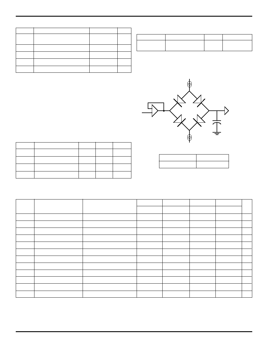
2905 drw 07
Signal
Cld
All Signals
25 pF
2905 tbl 09
Symbol
Parameter
Min.
Max.
Unit
V
IH
Input HIGH Voltage
3.0
--
V
V
IL
Input LOW Voltage
--
0
V
V
IHS
Input HIGH Voltage
3.5
--
V
V
ILS
Input LOW Voltage
--
0
V
AC TEST CONDITIONS R3041
2905 tbl 08
DC ELECTRICAL CHARACTERISTICS R3041 --
(T
C
= 0
∞
C to +85
∞
C, V
CC
= +5.0V
±
5%)
NOTES:
2905 tbl 10
1. V
IL
Min. = ≠3.0V for pulse width less than 15ns. V
IL
should not fall below ≠0.5 volts for larger periods.
2. V
IHS
and V
ILS
apply to CIkIn and
Reset
.
3. V
IH
should not be held above V
CC
+ 0.5 volts.
4. Guaranteed by design.

15
IDT79R3041 INTEGRATED RISController FOR LOW COST SYSTEMS
COMMERCIAL TEMPERATURE RANGE
ADV
ANCED
AC ELECTRICAL CHARACTERISTICS R3041
(1, 2, 3)
--
(T
C
= 0
∞
C to +85
∞
C, V
CC
= +5.0V
±
5%)
2905 tbl 11
16.67MHz
20MHz
25MHz
33MHz
Symbol
Signals
Description
Min.
Max.
Min.
Max.
Min.
Max.
Min.
Max.
Unit
t1
BusReq
,
Ack
,
BusError
,
RdCEn
Set-up to
SysClk
rising
11
--
8
--
5.5
--
5.5
--
ns
t1a
A/D
Set-up to
SysClk
falling
12
--
9
--
7
--
7
--
ns
t2
BusReq
,
Ack
,
BusError
,
RdCEn
Hold from
SysClk
rising
4
--
3
--
2.5
--
2.5
ns
t2a
A/D
Hold from
SysClk
falling
2
--
2
--
1
--
1
--
ns
t3
A/D, Addr, Diag, ALE,
Wr
Tri-state from
SysClk
rising
--
13
--
10
--
10
--
10
ns
Burst
/
WrNear
,
Rd
,
DataEn
(after driven condition)
t4
A/D, Addr, Diag, ALE,
Wr
Driven from
SysClk
falling
--
13
--
10
--
10
--
10
ns
Burst
/
WrNear
,
Rd
,
DataEn
(after tri-state condition)
t5
BusGnt
Asserted from
SysClk
rising
--
10
--
8
--
7
--
7
ns
t6
BusGnt
Negated from
SysClk
falling
--
10
--
8
--
7
--
7
ns
t7
Wr
,
Rd
,
Burst
/
WrNear
,
TC
Valid from
SysClk
rising
--
8
--
6
--
5
--
5
ns
t7a
A/D
Valid from
SysClk
rising
--
12
--
9
--
8
--
8
ns
t7b
Last
Valid from
SysClk
rising
--
12
--
9
--
8
--
8
ns
t8
ALE
Asserted from
SysClk
rising
--
5
--
4
--
4
--
4
ns
t9
ALE
Negated from
SysClk
falling
--
5
--
4
--
4
--
4
ns
t10
A/D
Hold from ALE negated
2
--
2
--
2
--
1.5
ns
t11
DataEn
Asserted from
SysClk
--
19
--
15
--
15
--
15
ns
t12
DataEn
Asserted from A/D tri-state
(4)
0
--
0
--
0
--
0
--
ns
t14
A/D
Driven from
SysClk
rising
(4)
0
--
0
--
0
--
0
--
ns
t15
Wr
,
Rd
,
DataEn
,
Burst
/
WrNear
,
Negated from
SysClk
falling
--
9
--
7
--
6
--
6
ns
Last
,
TC
t16
Addr(3:0),
BE 16(1:0)
Valid from
SysClk
--
11
--
8
--
7
--
7
ns
t17
Diag
Valid from
SysClk
--
15
--
12
--
11
--
11
ns
t18
A/D
Tri-state from
SysClk
--
13
--
10
--
10
--
10
ns
t19
A/D
SysClk
to data out
--
16
--
13
--
12
--
12
ns
t20
ClkIn
Pulse Width High
12
--
10
--
8
--
6.5
--
ns
t21
ClkIn
Pulse Width Low
12
--
10
--
8
--
6.5
--
ns
t22
ClkIn
Clock Period
30
250
25
250
20
250
15
250
ns
t23
Reset
Pulse Width from Vcc valid
200
--
200
--
200
--
200
--
µ
s
t24
Reset
Minimum Pulse Width
32
--
32
--
32
--
32
--
sys
t25
Reset
Set-up to
SysClk
falling
8
--
6
--
5
--
5
--
ns
t26
Int
Mode set-up to
Reset
rising
8
--
6
--
5
--
5
--
ns
t27
Int
Mode hold from
Reset
rising
2.5
--
2.5
--
2.5
--
2.5
--
ns
t28
SInt
, SBrCond
Set-up to
SysClk
falling
8
--
6
--
5
--
5
--
ns
t29
SInt
, SBrCond
Hold from
SysClk
falling
4
--
3
--
3
--
3
--
ns
t30
Int
, BrCond
Set-up to
SysClk
falling
8
--
6
--
5
--
5
--
ns
t31
Int
, BrCond
Hold from
SysClk
falling
4
--
3
--
3
--
3
--
ns
tsys
SysClk
Pulse Width
2*t22
2*t22
2*t22
2*t22
2*t22
2*t22
2*t22
2*t22
ns
t32
SysClk
Clock High Time
t22 - 2 t22 + 2 t22 - 2 t22 + 2 t22 - 2 t22 + 2 t22 - 2 t22 + 2
ns
t33
SysClk
Clock Low Time
t22 - 2 t22 + 2 t22 - 2 t22 + 2 t22 - 2 t22 + 2 t22 - 2 t22 + 2
ns
16
IDT79R3041 INTEGRATED RISController FOR LOW COST SYSTEMS
COMMERCIAL TEMPERATURE RANGE
ADV
ANCED
AC ELECTRICAL CHARACTERISTICS R3041 (CONT.)
16.67MHz
20MHz
25MHz
33MHz
Symbol
Signals
Description
Min.
Max.
Min.
Max.
Min.
Max.
Min.
Max.
Unit
t45
ExtDataEn
Tri-state from
SysClk
rising
--
13
--
10
--
10
--
10
ns
(after driven condition)
t46
ExtDataEn
Driven from
SysClk
falling
--
13
--
10
--
10
--
10
ns
(after driven condition)
t47
IOStrobe
Valid from
SysClk
falling
--
10
--
8
--
7
--
7
ns
t48
ExtDataEn
,
DataEn
Asserted from
SysClk
rising
--
15
--
12
--
9
--
9
ns
t49
ExtDataEn
Negated from
SysClk
rising
--
9
--
7
--
6
--
6
ns
t50
MemStrobe
Asserted from
SysClk
rising
--
19
--
15
--
15
--
15
ns
t51
MemStrobe
Negated from
SysClk
falling
--
19
--
15
--
15
--
15
ns
t52
MemStrobe
Asserted from Addr(3:0) valid
(4)
0
--
0
--
0
--
0
--
ns
tderate
All outputs
Timing deration for loading
--
0.5
--
0.5
--
0.5
--
0.5
ns/
over 25pF
(4, 5)
25pF
NOTES:
2905 tbl 12
1. All timings referenced to 1.5 Volts, with a rise and fall time of less than 2.5ns.
2. All outputs tested with 25pF loading.
3. The AC values listed here reference timing diagrams contained in the R3041 Hardware User's Manual.
4. Guaranteed by design.
5. This parameter is used to derate the AC timings according to the loading of the system. This parameter provides a deration for loads over the specified
test condition; that is, the deration factor is applied for each 25pF over the specified test load condition.
6. Timings t34 - t44 are reserved for other RISController family members.
RECOMMENDED OPERATING
TEMPERATURE AND SUPPLY VOLTAGE
OUTPUT LOADING FOR AC TESTING
ABSOLUTE MAXIMUM RATINGS
(1, 3)
RV3041
Symbol
Rating
Commercial
Unit
V
TERM
Terminal Voltage with
≠0.5 to +7.0
V
Respect to GND
T
C
Operating Case Temperature
0 to +85
∞
C
T
BIAS
Temperature Under Bias
≠55 to +125
∞
C
T
STG
Storage Temperature
≠55 to +125
∞
C
V
IN
Input Voltage
≠0.5 to +7.0
V
NOTES:
2905 tbl 06
1. Stresses greater than those listed under ABSOLUTE MAXIMUM RATINGS
may cause permanent damage to the device. This is a stress rating only
and functional operation of the device at these or any other conditions
above those indicated in the operational sections of this specification is not
implied. Exposure to absolute maximum rating conditions for extended
periods may affect reliability.
2. V
IN
minimum = ≠3.0V for pulse width less than 15ns.
V
IN
should not exceed V
CC
+0.5 Volts.
3. Not more than one output should be shorted at a time. Duration of the short
should not exceed 30 seconds.
Grade
Temperature
GND
V
CC
Commercial
0
∞
C to +85
∞
C
0V
3.3
±
5%
RV3041
(Case)
2905 tbl 07
-
+
To Device
Under Test
C
LD
-4mA
+4mA
V
REF
+1.5V
2905 drw 07
Signal
Cld
All Signals
25 pF
2905 tbl 09
Symbol
Parameter
Min.
Max.
Unit
V
IH
Input HIGH Voltage
3.0
--
V
V
IL
Input LOW Voltage
--
0
V
V
IHS
Input HIGH Voltage
3.0
--
V
V
ILS
Input LOW Voltage
--
0
V
AC TEST CONDITIONS RV3041
2905 tbl 08
17
IDT79R3041 INTEGRATED RISController FOR LOW COST SYSTEMS
COMMERCIAL TEMPERATURE RANGE
ADV
ANCED
ADV
ANCED
DC ELECTRICAL CHARACTERISTICS RV3041 -- (T
C
= 0
∞
C to +85
∞
C, V
CC
= +3.3V
±
5%)
16.67MHz
20MHz
25MHz
33MHz
Symbol
Parameter
Test Conditions
Min.
Max.
Min.
Max.
Min.
Max.
Min.
Max. Unit
V
OH
Output HIGH Voltage
V
CC
= Min., I
OH
= ≠4mA
2.4
--
2.4
--
2.4
--
2.4
--
V
V
OL
Output LOW Voltage
V
CC
= Min., I
OL
= 4mA
--
0.4
--
0.4
--
0.4
--
0.4
V
V
IH
Input HIGH Voltage
(3)
--
2.0
--
2.0
--
2.0
--
2.0
--
V
V
IL
Input LOW Voltage
(1)
--
--
0.8
--
0.8
--
0.8
--
0.8
V
V
IHS
Input HIGH Voltage
(2,3)
--
2.5
--
2.5
--
2.5
--
2.5
--
V
V
ILS
Input LOW Voltage
(1,2)
--
--
0.4
--
0.4
--
0.4
--
0.4
V
C
IN
Input Capacitance
(4)
--
--
10
--
10
--
10
--
10
pF
C
OUT
Output Capacitance
(4)
--
--
10
--
10
--
10
--
10
pF
I
CC
Operating Current
V
CC
= 3.3V, T
C
= 25
∞
C
--
130
--
150
--
180
--
225
mA
I
IH
Input HIGH Leakage
V
IH
= VCC
--
100
--
100
--
100
--
100
mA
I
IL
Input LOW Leakage
V
IL
= GND
≠100
--
≠100
--
≠100
--
≠100
--
mA
I
OZ
Output Tri-state Leakage
V
OH
= 2.4V, V
OL
= 0.5V
≠100
100
≠100
100
≠100
100
≠100
100
mA
NOTES:
2905 tbl 10
1. V
IL
Min. = ≠3.0V for pulse width less than 15ns. V
IL
should not fall below ≠0.5 volts for larger periods.
2. V
IHS
and V
ILS
apply to CIkIn and
Reset
.
3. V
IH
should not be held above V
CC
+ 0.5 volts.
4. Guaranteed by design.
AC ELECTRICAL CHARACTERISTICS RV3041
(1, 2, 3)
--
(T
C
= 0
∞
C to +85
∞
C, V
CC
= +3.3V
±
5%)
16.67MHz
20MHz
25MHz
33MHz
Symbol
Signals
Description
Min.
Max. Min.
Max. Min. Max. Min. Max. Unit
t1
BusReq
,
Ack
,
BusError
,
Set-up to
SysClk
rising
11
--
8
--
5.5
--
5.5
--
ns
RdCEn
t1a
A/D
Set-up to
SysClk
falling
12
--
9
--
7
--
7
--
ns
t2
BusReq
,
Ack
,
BusError
,
Hold from
SysClk
rising
4
--
3
--
2.5
--
2.5
--
ns
RdCEn
t2a
A/D
Hold from
SysClk
falling
2
--
2
--
1
--
1
--
ns
t3
A/D, Addr, Diag, ALE,
Wr
Tri-state from
SysClk
rising
--
13
--
10
--
10
--
10
ns
Burst/WrNear
,
Rd
,
DataEn
(after driven condition)
t4
A/D, Addr, Diag, ALE,
Wr
Driven from
SysClk
falling
--
13
--
10
--
10
--
10
ns
Burst/WrNear
,
Rd
,
DataEn
(after tri-state condition)
t5
BusGnt
Asserted from
SysClk
rising
--
10
--
8
--
7
--
7
ns
t6
BusGnt
Negated from
SysClk
falling
--
10
--
8
--
7
--
7
ns
t7
Wr
,
Rd
,
Burst/WrNear
, TC
Valid from
SysClk
rising
--
8
--
6
--
5
--
5
ns
t7a
A/D
Valid from
SysClk
rising
--
12
--
9
--
8
--
8
ns
t7b
Last
Valid from
SysClk
rising
--
12
--
9
--
8
--
8
ns
t8
ALE
Asserted from
SysClk
rising
--
5
--
4
--
4
--
4
ns
t9
ALE
Negated from
SysClk
falling
--
5
--
4
--
4
--
4
ns
t10
A/D
Hold from ALE negated
2
--
2
--
2
--
1.5
ns
t11
DataEn
Asserted from
SysClk
--
19
--
15
--
15
--
15
ns
t12
DataEn
Asserted from A/D tri-state
(4)
0
--
0
--
0
--
0
--
ns
t14
A/D
Driven from
SysClk
rising
(4)
0
--
0
--
0
--
0
--
ns
t15
Wr
,
Rd
,
DataEn
,
Negated from
SysClk
falling
--
9
--
7
--
6
--
6
ns
Burst/WrNear
, Last, TC
t16
Addr(3:0), BE 16(1:0)
Valid from
SysClk
--
11
--
8
--
7
--
7
ns
t17
Diag
Valid from
SysClk
--
15
--
12
--
11
--
11
ns
2905 tbl 11

18
IDT79R3041 INTEGRATED RISController FOR LOW COST SYSTEMS
COMMERCIAL TEMPERATURE RANGE
ADV
ANCED
16.67 MHz
20 MHz
25MHz
33MHz
Symbol
Signals
Description
Min.
Max.
Min.
Max.
Min.
Max.
Min.
Max.
Unit
t18
A/D
Tri-state from
SysClk
--
13
--
10
--
10
--
10
ns
t19
A/D
SysClk
to data out
--
16
--
13
--
12
--
12
ns
t20
ClkIn
Pulse Width High
12
--
10
--
8
--
6.5
--
ns
t21
ClkIn
Pulse Width Low
12
--
10
--
8
--
6.5
--
ns
t22
ClkIn
Clock Period
30
250
25
250
20
250
15
250
ns
t23
Reset
Pulse Width from Vcc valid
200
--
200
--
200
--
200
--
µ
s
t24
Reset
Minimum Pulse Width
32
--
32
--
32
--
32
--
sys
t25
Reset
Set-up to
SysClk
falling
8
--
6
--
5
--
5
--
ns
t26
Int
Mode set-up to
Reset
rising
8
--
6
--
5
--
5
--
ns
t27
Int
Mode hold from
Reset
rising
2.5
--
2.5
--
2.5
--
2.5
--
ns
t28
SInt
, SBrCond
Set-up to
SysClk
falling
8
--
6
--
5
--
5
--
ns
t29
SInt
, SBrCond
Hold from
SysClk
falling
4
--
3
--
3
--
3
--
ns
t30
Int
, BrCond
Set-up to
SysClk
falling
8
--
6
--
5
--
5
--
ns
t31
Int
, BrCond
Hold from
SysClk
falling
4
--
3
--
3
--
3
--
ns
tsys
SysClk
Pulse Width
2*t22
2*t22
2*t22
2*t22
2*t22
2*t22
2*t22
2*t22
ns
t32
SysClk
Clock High Time
t22 - 2
t22 + 2
t22 - 2 t22 + 2 t22 - 2 t22 + 2 t22 - 2 t22 + 2
ns
t33
SysClk
Clock Low Time
t22 - 2
t22 + 2
t22 - 2 t22 + 2 t22 - 2 t22 + 2 t22 - 2 t22 + 2
ns
t45
ExtDataEn
Tri-state from
SysClk
rising
--
13
--
10
--
10
--
10
ns
(after driven condition)
t46
ExtDataEn
Driven from
SysClk
falling
--
13
--
10
--
10
--
10
ns
(after driven condition)
t47
IOStrobe
Valid from
SysClk
falling
--
10
--
8
--
7
--
7
ns
t48
ExtDataEn
,
Asserted from
SysClk
rising
--
15
--
12
--
9
--
9
ns
t49
ExtDataEn
Negated from
SysClk
rising
--
9
--
7
--
6
--
6
ns
DataEn
t50
MemStrobe
Asserted from
SysClk
rising
--
19
--
15
--
15
--
15
ns
t51
MemStrobe
Negated from
SysClk
falling
--
19
--
15
--
15
--
15
ns
t52
MemStrobe
Asserted from Addr(3:0) valid
(4)
0
--
0
--
0
--
0
--
ns
tderate
All outputs
Timing deration for loading
--
0.5
--
0.5
--
0.5
--
0.5
ns/
over 25pF
(4, 5)
25pF
NOTES:
2905 tbl 12
1. All timings referenced to 1.5 Volts, with a rise and fall time of less than 2.5ns.
2. All outputs tested with 25pF loading.
3. The AC values listed here reference timing diagrams contained in the R3041 Hardware User's Manual.
4. Guaranteed by design.
5. This parameter is used to derate the AC timings according to the loading of the system. This parameter provides a deration for loads over the specified
test condition; that is, the deration factor is applied for each 25pF over the specified test load condition.
6. Timings t34 - t44 are reserved for other RISController family members.
AC ELECTRICAL CHARACTERISTICS RV3041 (CONT.)
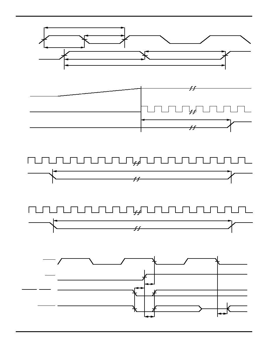
19
IDT79R3041 INTEGRATED RISController FOR LOW COST SYSTEMS
COMMERCIAL TEMPERATURE RANGE
Figure 11. Mode Selection and Negation of Reset
SysClk
Reset
t
25
t
26
Mode Vector Inputs:
SInt(2:0), Int(5:3)
t
27
Mode Vector Inputs:
Addr(3:0), BE16(1:0)
t
4
CPU Drives
External Device Drives Signals
2905 drw 12
Figure 10(b). Warm Reset Sequence (Internal Pull-Ups Used)
Figure 10(a). Warm Reset Sequence
Figure 9. Power-On Reset Sequence
Figure 8. RISController Family Clocking
ClkIn
SysClk
t
20
t
21
t
22
t
32
t
sys
t
33
2905 drw 08
V
CC
ClkIn
Reset
t
23
2905 drw 09
ClkIn
Reset
t
24
2905 drw 10
ClkIn
Reset
t
23
2905 drw 11

20
IDT79R3041 INTEGRATED RISController FOR LOW COST SYSTEMS
COMMERCIAL TEMPERATURE RANGE
Figure 12(a). Start of Read Timing with Non-Extended Address Hold Option
Figure 12(b). Start of Read Timing with Extended Address Hold Option
Addr
BE
SysClk
Rd
A/D(31:0)
ALE
Addr(3:2)
DataEn
Address
Memory
Turn
Bus
Sample
Data?
Cached?
I/D
t
7
t
14
t
18
t
10
t
8
t
9
t
12
t
17
t
17
t
11
Diag
t
16
t
7a
2905 drw 13
Addr
BE
SysClk
Rd
A/D(31:0)
ALE
Addr(3:2)
DataEn
Address
Memory
Extend
Address
Sample
Data?
Cached?
I/D
t
7
t
14
t
18
t
8
t
9
t
12
t
17
t
17
Diag
t
16
t
7a
2905 drw 14
t
48
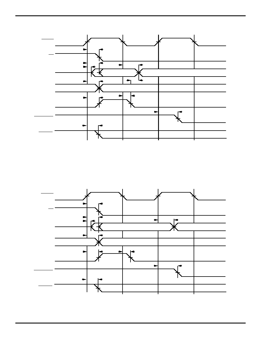
21
IDT79R3041 INTEGRATED RISController FOR LOW COST SYSTEMS
COMMERCIAL TEMPERATURE RANGE
Figure 12(d). Start of Write Timing with Extended Address Hold Option
Addr
BE
SysClk
Wr
A/D(31:0)
ALE
Addr(3:2)
Address
Memory
Extended
Address
End
Write?
t
7
t
14
t
19
t
8
t
9
t
48
ExtDataEn
WrNear
t
7
Data
Out
t
7a
t
16
2905 drw 16
Figure 12(c). Start of Write Timing with Non-Extended Address Hold Option
Addr
BE
SysClk
Wr
A/D(31:0)
ALE
Addr(3:2)
Address
Memory
Data
Phase
End
Write?
t
7
t
14
t
19
t
10
t
8
t
9
t
48
ExtDataEn
WrNear
t
7
Data
Out
t
7a
t
16
2905 drw 15
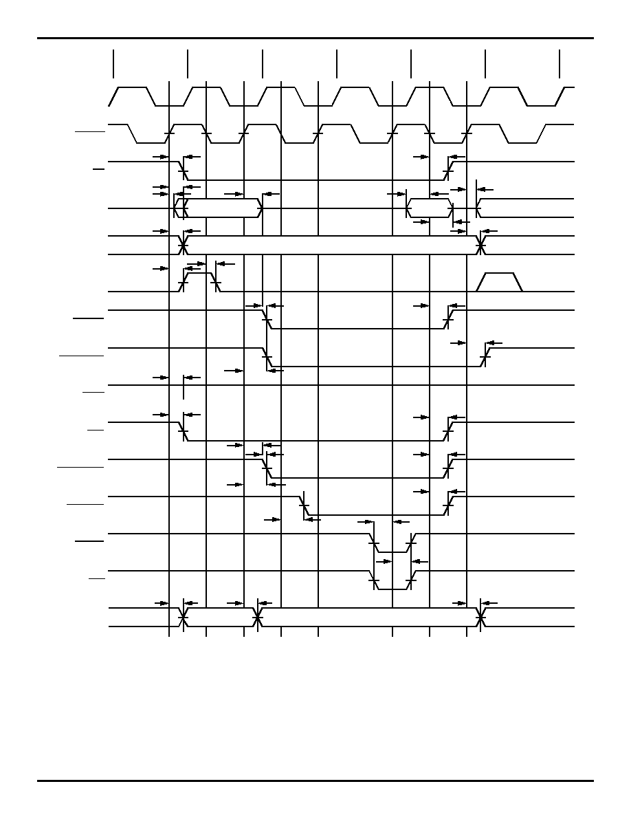
22
IDT79R3041 INTEGRATED RISController FOR LOW COST SYSTEMS
COMMERCIAL TEMPERATURE RANGE
Figure 13. Single Datum Read
PhiClk
SysClk
Rd
A/D(31:0)
ALE
Addr(3:2)
Addr
BE
DataEn
RdCEn
Word Address
Stall
Stall
Stall
Stall
Stall
Fixup
Ack
Burst
Diag
Start
Read
Extended
Address
Sample
Data
End
Read
Run/
Stall
Ack/
RdCEn
Cached?
I/D
Data Input
t
7
t
14
t
8
t
7
t
12
t
1
t
2
t
15
t
2a
t
15
t
1a
t
14
t
17
t
17
t
18
t
16
ExtDataEn
t
49
t
48
Last
t
15
MemStrobe
IOStrobe
t
47
t
50
t
17
t
16
t
18
t
12
t
15
t
51
Ack/
RdCEn
?
Ack/
RdCEn
?
t
9
t
7a
2905 drw 17
t
7b
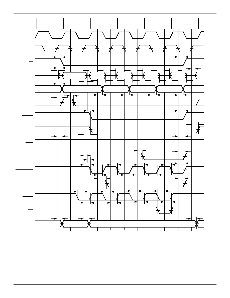
23
IDT79R3041 INTEGRATED RISController FOR LOW COST SYSTEMS
COMMERCIAL TEMPERATURE RANGE
PhiClk
SysClk
Rd
A/D(31:0)
ALE
Addr(3:0)
Addr
DataEn
RdCEn
'nn00'
Stall
Stall
Stall
Ack
Last
Diag
Start
Read
Extended
Address
Sample
Data
New
Transaction
Run/
Stall
Ack/
RdCEn
Cached?
t
7
t
14
t
8
t
9
t
7b
t
12
t
2
t
17
t
17
t
18
t
15
Byte 0
t
2a
t
1a
t
14
t
15
Byte 1
t
2a
t
1a
Byte 2
t
2a
t
1a
Byte 3
t
2a
t
1a
'nn01'
'nn10'
'nn11'
t
1
t
2
t
1
t
2
t
1
t
2
t
16
t
16
t
16
Sample
Data
Sample
Data
Sample
Data
RdCEn
RdCEn
RdCEn
I/D
t
16
ExtDataEn
t
49
t
48
Burst
t
7
MemStrobe
IOStrobe
t
50
t
47
t
50
t
51
t
50
t
50
t
51
t
51
t
16
t
1
t
15
t
15
t
17
Stall
Stall
Stall
Fixup
t
18
t
12
t
15
t
51
t
7a
2905 drw 18
Figure 14. Mini-burst read of 32-bit datum from 8-bit wide memory port
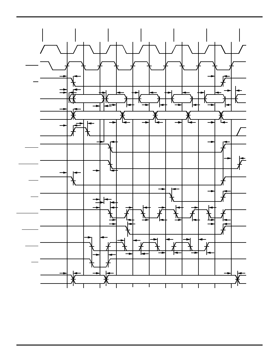
24
IDT79R3041 INTEGRATED RISController FOR LOW COST SYSTEMS
COMMERCIAL TEMPERATURE RANGE
PhiClk
SysClk
Rd
A/D(31:0)
ALE
Addr(3:2)
Addr
BE
DataEn
RdCEn
'00'
Stall
Stall
Stall
Refill/
Fixup
Ack
Last
Diag
Start
Read
Extended
Address
Sample
Data
New
Transaction
Run/
Stall
Ack/
RdCEn
Cached
t
7
t
14
t
8
t
9
t
7b
t
12
t
1
t
2
t
17
t
17
t
18
t
15
Word 0
t
2a
t
1a
t
14
t
15
Word 1
t
2a
t
1a
Word 2
t
2a
t
1a
Word 3
t
2a
t
1a
'01'
'10'
'11'
t
1
t
2
t
1
t
2
t
1
t
2
Refill/
Stream/
Fixup
Refill/
Stream/
Fixup
Refill/
Stream/
Fixup
t
16
t
16
t
16
Sample
Data
Sample
Data
Sample
Data
RdCEn
RdCEn
RdCEn
I/D
Word 0
Word 1
Word 2
Word 3
t
16
ExtDataEn
t
49
t
48
Burst
t
7
MemStrobe
IOStrobe
t
50
t
47
t
50
t
51
t
50
t
50
t
51
t
51
t
16
t
17
t
15
t
15
t
51
t
18
t
12
t
7a
2905 drw 19
Figure 15. R3041 Quad Word Read
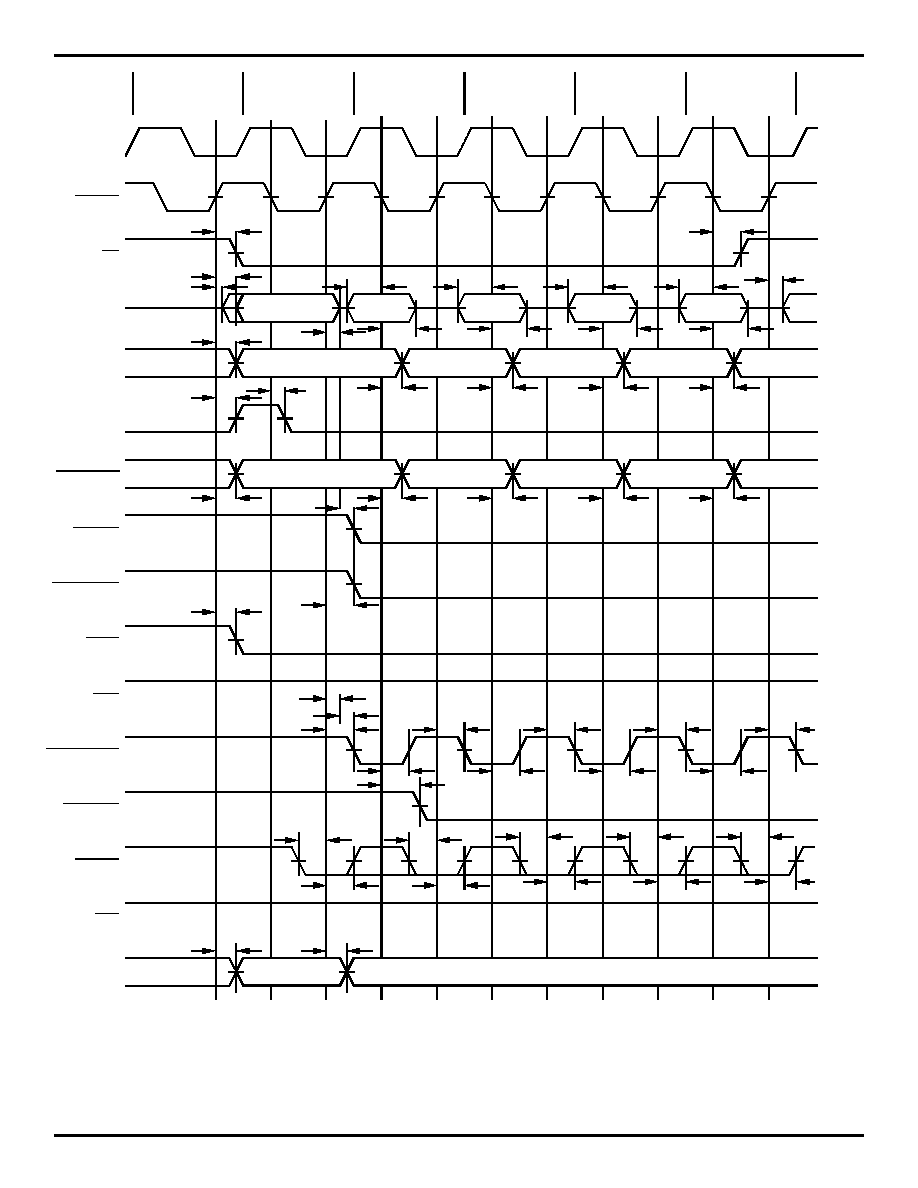
25
IDT79R3041 INTEGRATED RISController FOR LOW COST SYSTEMS
COMMERCIAL TEMPERATURE RANGE
Figure 16(a). Quad Word Read to 16-bit wide Memory Port
PhiClk
SysClk
Rd
A/D(31:0)
ALE
Addr(3:1)
Addr
DataEn
RdCEn
'000'
Stall
Stall
Stall
Ack
Last
Diag
Start
Read
Extended
Address
Sample
Data
Run/
Stall
Cached
t
7
t
14
t
8
t
9
t
12
t
17
t
17
t
18
t
15
Halfword 0
t
2a
t
1a
t
14
Halfword 1
t
2a
t
1a
Halfword 2
t
2a
t
1a
Halfword 3
t
2a
t
1a
'001'
'010'
'011'
t
1
t
2
t
1
t
2
t
1
t
2
t
16
t
16
t
16
Sample
Data
Sample
Data
Sample
Data
RdCEn
RdCEn
RdCEn
I/D
t
16
ExtDataEn
t
48
Burst
t
7
MemStrobe
IOStrobe
t
50
t
47
t
51
t
50
t
51
t
51
t
16
'100'
t
51
t
1
t
2
BE16(1:0)
'00'
'00'
'00'
'00'
t
16
t
16
t
16
t
16
'00'
RdCEn
Stall
Stall
Stall
Stall
t
1
t
2
RdCEn
t
16
t
50
t
50
t
50
t
18
t
12
t
7a
2905 drw 20
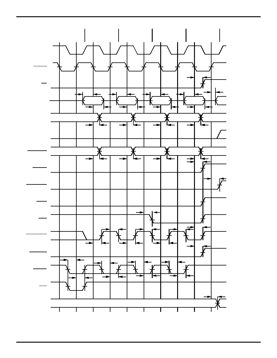
26
IDT79R3041 INTEGRATED RISController FOR LOW COST SYSTEMS
COMMERCIAL TEMPERATURE RANGE
Figure 16(b). End of Quad Word read from 16-bit Wide Memory Port
PhiClk
SysClk
Rd
A/D(31:0)
ALE
Addr(3:1)
DataEn
RdCEn
'100'
Stall
Refill/
Fixup
Ack
Last
Diag
Sample
Data
New
Transaction
Ack/
RdCEn
t
1
t
2
t
15
Halfword 4
t
2a
t
1a
t
14
t
15
Halfword 5
t
2a
t
1a
Halfword 6
t
2a
t
1a
Halfword 7
t
2a
t
1a
'101'
'110'
'111'
t
1
t
2
t
1
t
2
t
1
t
2
Refill/
Stream/
Fixup
Refill/
Stream/
Fixup
Refill/
Stream/
Fixup
t
16
t
16
t
16
Sample
Data
Sample
Data
Sample
Data
RdCEn
RdCEn
RdCEn
Word 0
Word 1
Word 2
Word 3
Stall
I/D
t
16
ExtDataEn
t
49
Burst
t
7b
MemStrobe
IOStrobe
t
17
t
50
t
51
t
50
t
51
t
50
t
51
BE16(1:0)
'00'
'00'
'00'
'00'
t
16
t
16
t
16
t
16
t
51
t
15
2905 drw 21
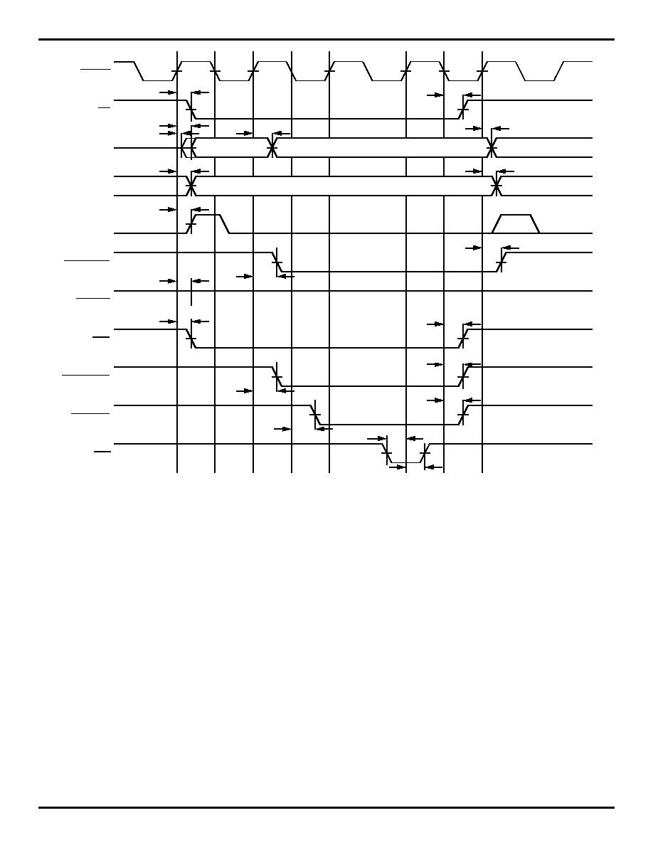
27
IDT79R3041 INTEGRATED RISController FOR LOW COST SYSTEMS
COMMERCIAL TEMPERATURE RANGE
SysClk
Wr
A/D(31:0)
ALE
Addr(3:2)
Addr
BE
Word Address
Ack
WrNear
Start
Write
Extended
Address
Data Out/
Ack?
Ack?
Negate
Write
New
Transfer
Ack
Data Output
t
7a
t
14
t
8
t
7
t
1
t
2
t
15
t
14
t
19
t
16
ExtDataEn
t
49
t
11
Last
t
15
MemStrobe
IOStrobe
t
47
t
50
t
16
t
15
t
51
t
7
2905 drw 22
t
7b
Figure 17. Basic Write to 32-bit Memory Port
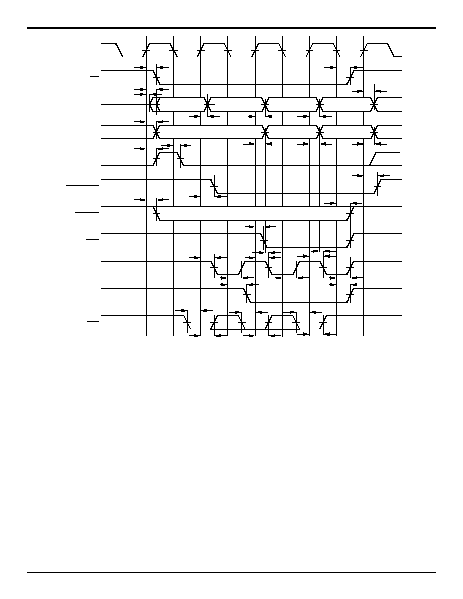
28
IDT79R3041 INTEGRATED RISController FOR LOW COST SYSTEMS
COMMERCIAL TEMPERATURE RANGE
SysClk
Wr
A/D(31:0)
ALE
Addr(3:0)
Addr
Ack
'nnnn'
Last
Start
Write
Extended
Address
New
Transaction
Ack
t
7
t
14
t
8
t
9
t
1
t
2
t
19
t
15
t
14
'nnnn+1'
t
1
t
16
Ack
t
16
ExtDataEn
t
49
t
48
WrNear
t
7
MemStrobe
IOStrobe
t
50
t
47
t
51
t
50
t
2
t
7b
t
16
'nnnn+2'
t
16
t
50
t
1
t
2
Ack
t
51
Byte N
t
19
t
19
Byte N+1
Byte N+2
Negate
Write
t
15
t
51
t
15
t
52
t
52
t
7a
2905 drw 23
Figure 18. Tri-Byte Mini-burst Write to 8-bit Port
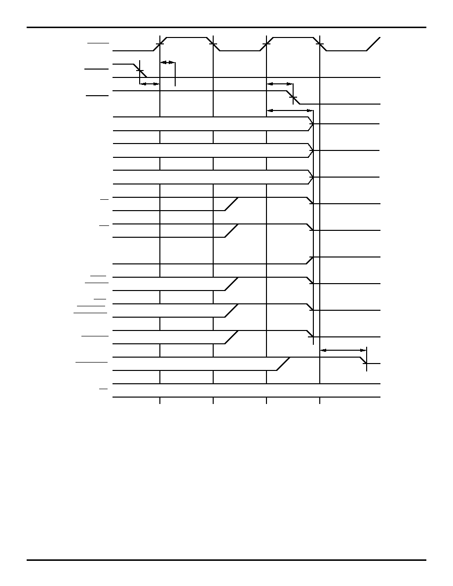
29
IDT79R3041 INTEGRATED RISController FOR LOW COST SYSTEMS
COMMERCIAL TEMPERATURE RANGE
SysClk
BusReq
BusGnt
A/D(31:0)
Addr(3:0)
Diag
Rd
Wr
ALE
Burst/
WrNear
t
1
t
2
t
5
t
3
Last,
BE16(1:0),
MemStrobe
IOStrobe
t
45
ExtDataEn
TC
2905 drw 24
Figure 19. Request and Relinquish of R3041 Bus to External Master
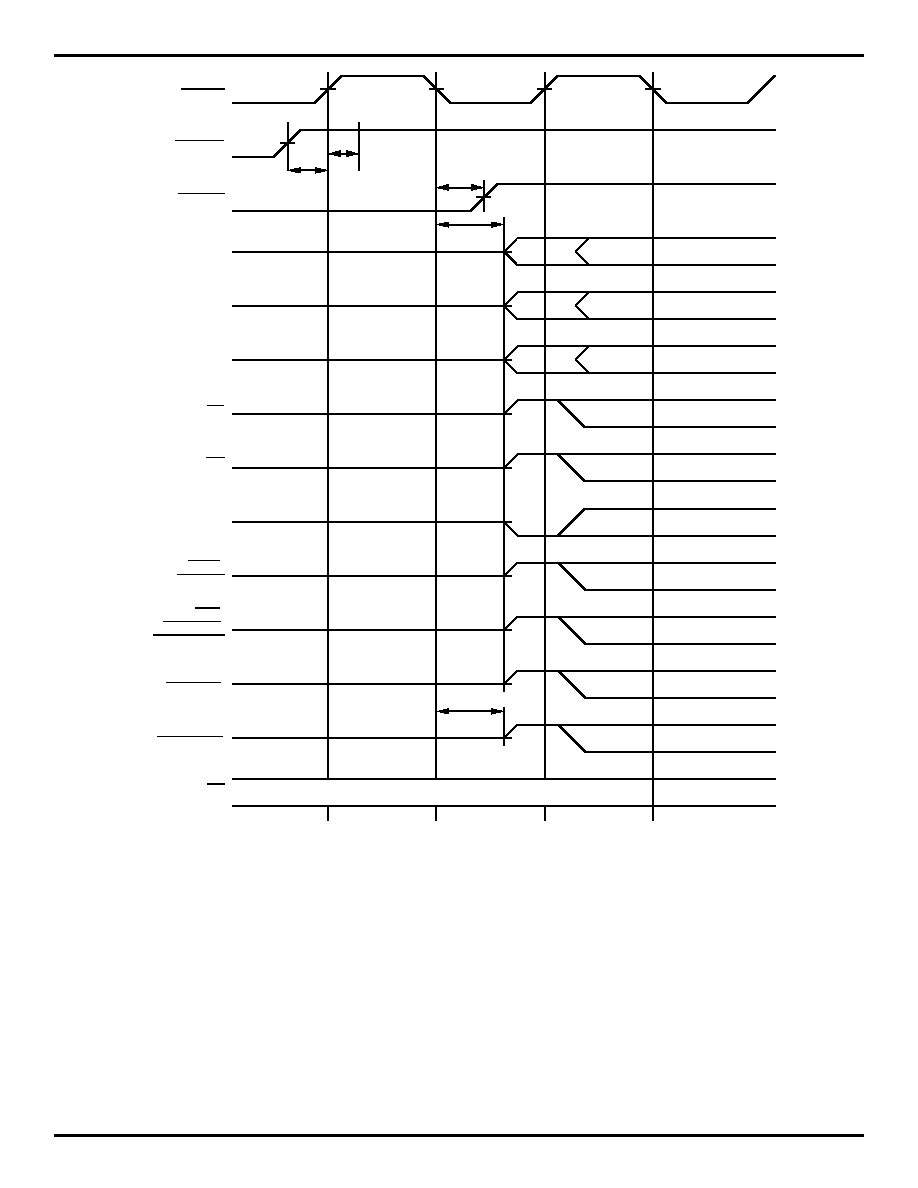
30
IDT79R3041 INTEGRATED RISController FOR LOW COST SYSTEMS
COMMERCIAL TEMPERATURE RANGE
SysClk
BusReq
BusGnt
A/D(31:0)
Addr(3:0)
Diag
Rd
Wr
ALE
Burst/
WrNear
t
1
t
2
t
6
t
4
Last,
BE16(1:0)
MemStrobe
IOStrobe
TC
ExtDataEn
t
46
2905 drw 25
Figure 20. R3041 Regaining Bus Mastership
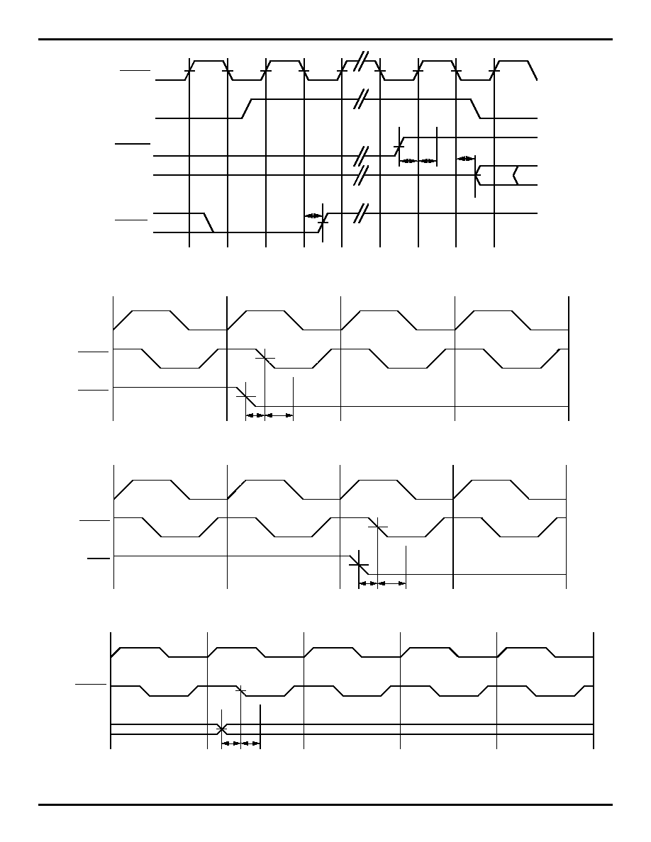
31
IDT79R3041 INTEGRATED RISController FOR LOW COST SYSTEMS
COMMERCIAL TEMPERATURE RANGE
Figure 21. R3041 DMA Pulse Protocol
Figure 22. Synchronized Interrupt Input Timing
Figure 24. Synchronized Branch Condition Input Timing
Figure 23. Direct Interrupt Input Timing
Phi
SysClk
Int(n)
Exception Vector
Run Cycle
2905 drw 28
t
30
t
31
Phi
SysClk
SInt(n)
Exception Vector
Run Cycle
2905 drw 27
t
29
t
28
SysClk
CPU Bus
Request
BusReq
A/D(31:0)
BusGnt
t
6
t
4
t
1
t
2
2905 drw 26
Phi
SysClk
SBrCond(n)
BCzT/F Instruction
Capture BrCond
2905 drw 29
Run Cycle
t
28
t
29
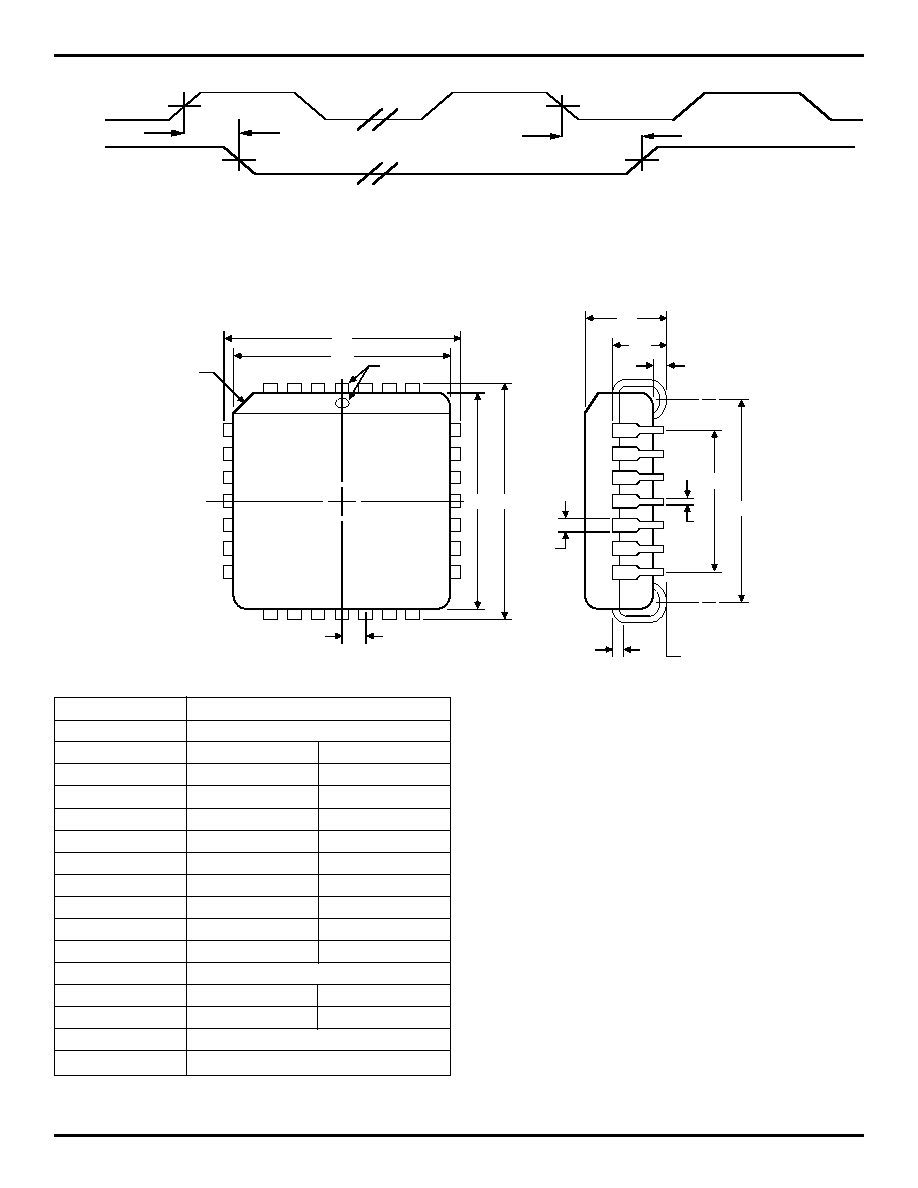
32
IDT79R3041 INTEGRATED RISController FOR LOW COST SYSTEMS
COMMERCIAL TEMPERATURE RANGE
Figure 25.
TC
TC
TC
TC
TC
Output
SysClk
TC
t
7
t
15
2905 drw 30
DWG #
J84-1
# of Leads
84
Symbol
Min.
Max.
A
165
.180
A1
.095
.115
B
.026
.032
b1
.013
.021
C
.020
.040
C1
.008
.012
D
1.185
1.195
D1
1.150
1.156
D2/E2
1.090
1.130
D3/E3
1.000 REF
E
1.185
1.195
E1
1.150
1.156
e
.050 BSC
ND/NE
21
2905 tbl 13
2874 drw 02
D
D1
PIN 1
E1
E
e
45
∞
x .045
B
C1
SEATING PLANE
D2/E2
D3/E3
b1
C
A
A1
2905 drw 31
84 LEAD PLCC (SQUARE)
NOTES:
1. All dimensions are in inches, unless otherwise noted.
2. BSC--Basic lead Spacing between Centers.
3. D & E do not include mold flash or protutions.
4. Formed leads shall be planar with respect to one another and within .004"
at the seating plane.
5. ND & NE represent the number of leads in the D & E directions respec-
tively.
6. D1 & E1 should be measured from the bottom of the package.
7. PLCC is pin & form compatible with MQUAD; the MQUAD package is used
in other RISController family members.
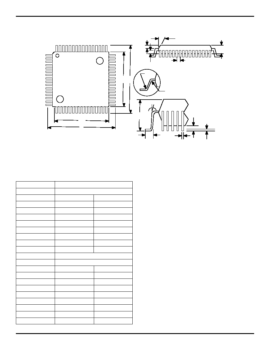
33
IDT79R3041 INTEGRATED RISController FOR LOW COST SYSTEMS
COMMERCIAL TEMPERATURE RANGE
100-PIN TQFP
1
1 0 0
E1 E
D1
D
A 1
A 2
e
Draft Angle = 12
∞
A 3
B
1 0 0 - P i n
TQFP
Standoff 0.05 Min
Max 0.102 Lead
Coplanarity
6
∞
±
4
∞
0.30 Rad Typ.
0.20 Rad Typ.
L
A
DWG #
TQFP
# of Leads
100
Symbol
Min.
Max.
A
--
1.60
A1
0.5
0.15
A2
1.35
1.45
D
15.75
16.25
D1
13.95
14.05
E
15.75
16.25
E1
13.95
14.05
L
0.45
0.70
N
100
e
0.50BSC
b
0.17
0.27
ccc
--
0.08
ddd
--
0.08
R
0.08
0.20
R1
0.08
--
0
7.0
1
11.0
13.0
2
11.0
13.0
c
0.09
0.16
2905 tbl 14
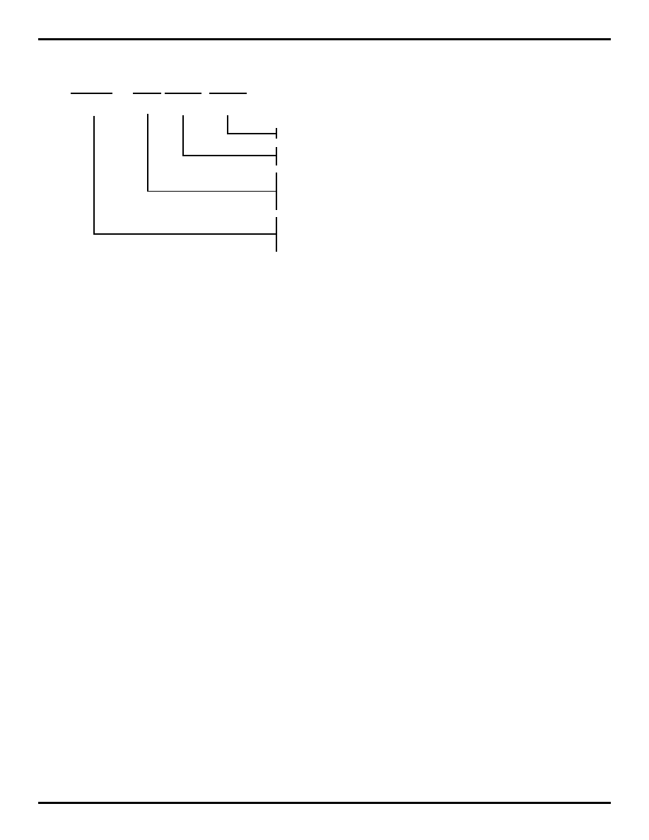
34
IDT79R3041 INTEGRATED RISController FOR LOW COST SYSTEMS
COMMERCIAL TEMPERATURE RANGE
ORDERING INFORMATION
VALID COMBINATIONS
IDT 79R3041 - 16
TQFP, PLCC Package
79R3041 - 20
TQFP, PLCC Package
79R3041 - 25
TQFP, PLCC Package
79R3041 - 33
PLCC Package Only
79RV3041 - 16
TQFP, PLCC Package
79RV3041 - 20
TQFP, PLCC Package
79RV3041 - 25
TQFP, PLCC Package
79RV3041 - 33
TQFP, PLCC Package
IDT
XXXXX
Device Type
XX
Speed
X
Package
--
X
Process/
Temp. Range
Blank
'J'
'PF'
'16'
'20'
'25'
'33'
79R3041
79RV3041
Commercial Temperature
Range
84-Pin PLCC
100-Pin TQFP
16.67MHz
20.00MHz
25.00MHz
33.00MHz
5.0V Integrated RISController for
Low-Cost Systems
3.3V Integrated RISController for
Low-Cost Systems
2905 drw 32