2703 drw 01
PD
0
31
29
9
11
13
15
17
19
21
23
25
1
3
5
7
27
33
63
61
41
43
45
47
49
51
53
55
57
35
37
39
59
PD
1
≠ GND
≠ GND
32
30
28
8
10
12
14
16
18
20
22
24
2
4
6
26
34
64
62
42
44
46
48
50
52
54
56
58
36
38
40
60
GND
CS
3
A
16
I/O
16
I/O
17
I/O
18
I/O
19
A
10
A
11
A
12
A
13
I/O
20
I/O
21
I/O
22
I/O
23
GND
I/O
0
I/O
1
I/O
2
I/O
3
V
CC
A
7
A
8
A
9
I/O
4
I/O
5
I/O
6
WE
I/O
7
CS
1
PD
0
A
14
CS
4
A
17
OE
I/O
24
I/O
25
I/O
26
I/O
27
A
3
A
4
A
5
V
CC
A
6
I/O
28
I/O
29
I/O
30
I/O
31
PD
1
GND
I/O
8
I/O
9
I/O
10
I/O
11
A
0
A
1
A
2
I/O
12
I/O
13
I/O
14
I/O
15
GND
CS
2
A
15
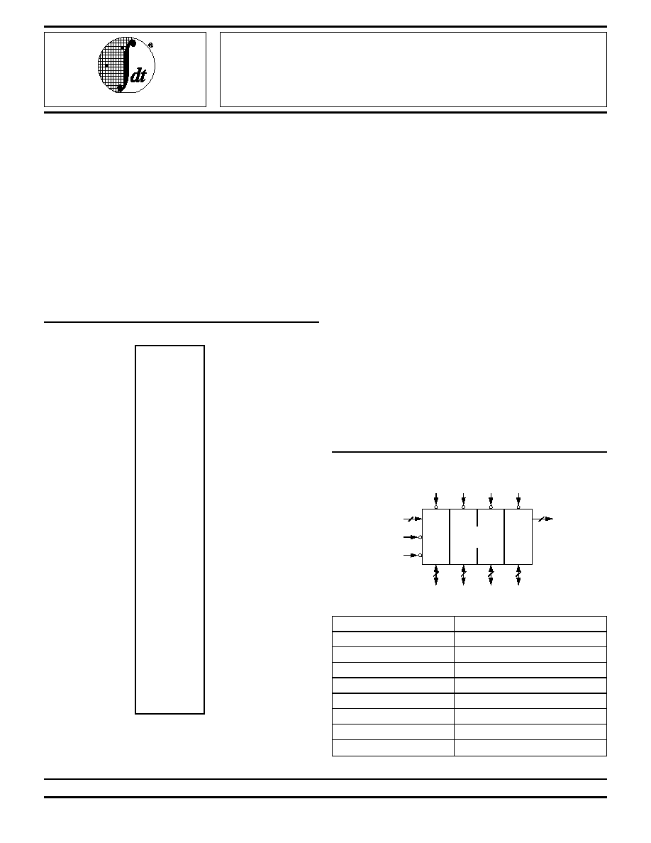
FEATURES:
∑ High density 1 megabyte static RAM module
(IDT7MP4145 upgradeable to 4 megabyte, IDT7MP4120)
∑ Low profile 64 pin ZIP (Zig-zag In-line vertical Package)
or 64 pin SIMM (Single In-line Memory Module) for
IDT7MP4045 and 72 pin SIMM (Single In-line Memory
Module) for IDT7MP4145
∑ Very fast access time: 15ns (max.)
∑ Surface mounted plastic components on an epoxy
laminate (FR-4) substrate
∑ Single 5V (
±
10%) power supply
∑ Multiple GND pins and decoupling capacitors for maxi-
mum noise immunity
∑ Inputs/outputs directly TTL-compatible
PIN NAMES
I/O
0
≠
31
Data Inputs/Outputs
A
0
≠
17
Addresses
CS
1≠4
Chip Selects
WE
Write Enable
OE
Output Enable
PD
0≠1
Depth Identification
V
CC
Power
GND
Ground
NC
No Connect
2703 tbl 01
Integrated Device Technology, Inc.
COMMERCIAL TEMPERATURE RANGE
SEPTEMBER 1996
©
1996 Integrated Device Technology, Inc.
DSC-2703/7
1
The IDT logo is a registered trademark of Integrated Device Technology Inc.
NOTE:
1. Pins 2 and 3 (PD
0
and PD
1
) are read by the user to determine the density
of the module. If PD
0
reads GND and PD
1
reads GND, then the module
has a 256K depth.
DESCRIPTION:
The IDT7MP4045/4145 is a 256K x 32 static RAM module
constructed on an epoxy laminate (FR-4) substrate using 8
256K x 4 static RAMs in plastic SOJ packages. Availability of
four chip select lines (one for each group of two RAMs)
provides byte access. The IDT7MP4045 is available with
access time as fast as 10ns with minimal power consumption.
The IDT7MP4045 is packaged in a 64 pin FR-4 ZIP (Zig-
zag In-line vertical Package)or a 64 pin SIMM (Single In-line
Memory Module) where as the 7MP4145 is packaged in a 72
pin SIMM (Single In-line Memory Module). The 4045 ZIP
configuration allows 64 pins to be placed on a package 3.65
inches long and 0.365 inches wide. The 7MP4045 ZIP is only
0.585 inches high, this low profile package is ideal for systems
with minimum board spacing while the SIMM configuration
allows use of edge mounted sockets to secure the module.
All inputs and outputs of the IDT7MP4045/4145 are TTL-
compatible and operate from a single 5V supply. Full asyn-
chronous circuitry requires no clocks or refresh for operation
and provides equal access and cycle times for ease of use.
Identification pins are provided for applications in which
different density versions of the module are used. In this way,
the target system can read the respective levels of PD
pins
to
determine a 256K depth.
The contact pins are plated with 100 micro-inches of nickel
covered by 30 micro-inches minimum of selective gold.
PIN CONFIGURATION ≠ 7MP4045
(1)
ZIP, SIMM
TOP VIEW
FUNCTIONAL BLOCK DIAGRAM
OE
WE
2703 drw 02
8
18
256K x 32
RAM
8
8
8
2
CS
1
CS
2
CS
3
CS
4
ADDRESS
I/O
0-31
PD
IDT7MP4045
IDT7MP4145
256K x 32
CMOS STATIC RAM MODULE
15.2
IDT7MP4045/7MP4145
256K x 32 CMOS STATIC RAM MODULE
COMMERCIAL TEMPERATURE RANGE
15.2
2
RECOMMENDED OPERATING
TEMPERATURE AND SUPPLY VOLTAGE
Ambient
Grade
Temperature
GND
V
CC
Commercial
0
∞
C to +70
∞
C
0V
5.0V
±
10%
2703 tbl 04
CAPACITANCE
(T
A
= +25
∞
C, F = 1.0MHz)
Symbol
Parameter
(1)
Conditions
Max.
Unit
C
IN(C)
Input Capacitance
V
(IN)
= 0V
20
pF
(
CS
)
C
IN(A)
Input Capacitance
V
(IN)
= 0V
70
pF
(Address & Control)
C
I/O
I/O Capacitance
V
(OUT)
= 0V
12
pF
NOTE:
2703 tbl 02
1. This parameter is guaranteed by design but not tested.
RECOMMENDED DC OPERATING
CONDITIONS
Symbol
Parameter
Min.
Typ.
Max.
Unit
V
CC
Supply Voltage
4.5
5.0
5.5
V
GND
Supply Voltage
0
0
0
V
V
IH
Input High Voltage
2.2
--
6.0
V
V
IL
Input Low Voltage
≠0.5
(1)
--
0.8
V
NOTE:
2703 tbl 03
1. V
IL
(min) = ≠1.5V for pulse width less than 10ns.
TRUTH TABLE
Mode
CS
CS OE
OE WE
WE
Output
Power
Standby
H
X
X
High-Z
Standby
Read
L
L
H
DATA
OUT
Active
Write
L
X
L
DATA
IN
Active
Read
L
H
H
High-Z
Active
2703 tbl 05
ABSOLUTE MAXIMUM RATINGS
(1)
Symbol
Rating
Value
Unit
V
TERM
Terminal Voltage with
≠0.5 to +7.0
V
Respect to GND
T
A
Operating Temperature
0 to +70
∞
C
T
BIAS
Temperature Under Bias
≠10 to +85
∞
C
T
STG
Storage Temperature
≠55 to +125
∞
C
I
OUT
DC Output Current
50
mA
NOTE:
2703 tbl 06
1. Stresses greater than those listed under ABSOLUTE MAXIMUM
RATINGS may cause permanent damage to the device. This is a stress
rating only and functional operation of the device at these or any other
conditions above those indicated in the operational sections of this
specification is not implied. Exposure to absolute maximum rating
conditions for extended periods may affect reliability.
PIN CONFIGURATION ≠ 7MP4145
(1)
SIMM
TOP VIEW
NOTE:
1. Pins 3,4,6,and 7 (PD
0
-
3
) are read by the user to determine the density of
the module. If PD
0
, PD
1
read GND and PD
2,
PD
3
read OPEN, then the
module has a 256K depth.
1
3
5
7
9
11
13
15
17
19
21
23
25
27
29
31
33
35
37
39
41
43
45
47
49
51
53
55
57
59
61
63
65
67
69
71
2
4
6
8
10
12
14
16
18
20
22
24
26
28
30
32
34
36
38
40
42
44
46
48
50
52
54
56
58
60
62
64
66
68
70
72
NC
PD
2
GND
PD
1
I/O
8
I/O
9
I/O
10
I/O
11
A
0
A
1
A
2
I/O
12
I/O
13
I/O
14
I/O
15
GND
A
15
CS
2
CS
4
A
17
OE
I/O
24
I/O
25
I/O
26
I/O
27
A
3
A
4
A
5
V
CC
A
6
I/O
28
I/O
29
I/O
30
I/O
31
NC
NC
NC
PD
3
PD
0
I/O
0
I/O
1
I/O
2
I/O
3
V
CC
A
7
A
8
A
9
I/O
4
I/O
5
I/O
6
I/O
7
WE
A
14
CS
1
CS
3
A
16
GND
I/O
16
I/O
17
I/O
18
I/O
19
A
10
A
11
A
12
A
13
I/O
20
I/O
21
I/O
22
I/O
23
GND
NC
NC
PD
0
- GND
PD
1
- GND
PD
2
- OPEN
PD
3
- OPEN
2703 drw 15
15.2
3
IDT7MP4045/7MP4145
256K x 32 CMOS STATIC RAM MODULE
COMMERCIAL TEMPERATURE RANGE
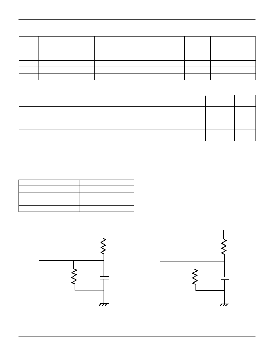
Figure 1. Output Load
*Includes scope and jig.
Figure 2. Output Load
(for t
OLZ
,t
OHZ
, t
CHZ
, t
CLZ
, t
WHZ
, t
OW
)
+5 V
480
30 pF*
DATA
OUT
255
2703 drw 03
+5 V
480
5 pF*
DATA
OUT
255
2703 drw 04
AC TEST CONDITIONS
Input Pulse Levels
GND to 3.0V
Input Rise/Fall Times
5ns
Input Timing Reference Levels
1.5V
Output Reference Levels
1.5V
Output Load
See Figures 1-4
2703 tbl 09
Symbol
Parameter
Test Conditions
Max.
Unit
I
CC
Dynamic Operating
f = f
MAX
;
CS
= V
IL
1360
mA
Current
V
CC
= Max.; Output Open
I
SB
Standby Supply
CS
V
IH,
V
CC
= Max.
480
mA
Current
Outputs Open, f = f
MAX
I
SB1
Full Standby
CS
V
CC
≠ 0.2V; f = 0
120
mA
Supply Current
V
IN
> V
CC
≠ 0.2V or < 0.2V
2703 tbl
2703 tbl 07
DC ELECTRICAL CHARACTERISTICS
(V
CC
= 5.0V
±
10%, T
A
= 0
∞
C to +70
∞
C)
Symbol
Parameter
Test Conditions
Min.
Max.
Unit
|I
LI
|
Input Leakage
V
CC
= Max.; V
IN
= GND to V
CC
--
80
µ
A
(Address and Control)
|I
LI
|
Input Leakage (Data)
V
CC
= Max.; V
IN
= GND to V
CC
--
10
µ
A
|I
LO
|
Output Leakage
V
CC
= Max.;
CS
= V
IH
, V
OUT
= GND to V
CC
--
10
µ
A
V
OL
Output LOW
V
CC
= Min., I
OL
= 8mA
--
0.4
V
V
OH
Output HIGH
V
CC
= Min., I
OH
= ≠4mA
2.4
--
V
IDT7MP4045/7MP4145
256K x 32 CMOS STATIC RAM MODULE
COMMERCIAL TEMPERATURE RANGE
15.2
4
AC ELECTRICAL CHARACTERISTICS
(V
CC
= 5V
±
10%, T
A
= 0
∞
C to +70
∞
C)
'4045SxxZ, '4045/4145SxxM
≠15
≠20
Symbol
Parameter
Min.
Max.
Min.
Max.
Unit
Read Cycle
t
RC
Read Cycle Time
15
--
20
--
ns
t
AA
Address Access Time
--
15
--
20
ns
t
ACS
Chip Select Access Time
--
15
--
20
ns
t
CLZ
(1)
Chip Select to Output in Low-Z
3
--
5
--
ns
t
OE
Output Enable to Output Valid
--
8
--
10
ns
t
OLZ
(1)
Output Enable to Output in Low-Z
0
--
0
--
ns
t
CHZ
(1)
Chip Deselect to Output in High-Z
--
8
--
10
ns
t
OHZ
(1)
Output Disable to Output in High-Z
--
8
--
10
ns
t
OH
Output Hold from Address Change
3
--
3
--
ns
t
PU
(1)
Chip Select to Power-Up Time
0
--
0
--
ns
t
PD
(1)
Chip Deselect to Power-Down Time
--
15
--
20
ns
Write Cycle
t
WC
Write Cycle Time
15
--
20
--
ns
t
CW
Chip Select to End-of-Write
12
--
15
--
ns
t
AW
Address Valid to End-of-Write
12
--
15
--
ns
t
AS
Address Set-up Time
0
--
0
--
ns
t
WP
Write Pulse Width
12
--
15
--
ns
t
WR
Write Recovery Time
0
--
0
--
ns
t
WHZ
(1)
Write Enable to Output in High-Z
--
8
--
13
ns
t
DW
Data to Write Time Overlap
10
--
12
--
ns
t
DH
Data Hold from Write Time
0
--
0
--
ns
t
OW
(1)
Output Active from End-of-Write
0
--
0
--
ns
NOTE:
2703 tbl 11
1. This parameter is guaranteed by design but not tested.
15.2
5
IDT7MP4045/7MP4145
256K x 32 CMOS STATIC RAM MODULE
COMMERCIAL TEMPERATURE RANGE
TIMING WAVEFORM OF READ CYCLE NO. 1
(1)
TIMING WAVEFORM OF READ CYCLE NO. 2
(1,2,4)
TIMING WAVEFORM OF READ CYCLE NO. 3
(1,3,4)
OE
t
AA
t
OH
ADDRESS
t
RC
CS
DATA OUT
t
ACS
t
OHZ
(5)
t
CHZ
(5)
t
OLZ (5)
2703 drw 07
t
CLZ
(5)
t
OE
2703 drw 08
t
AA
t
OH
t
OH
DATA
OUT
ADDRESS
t
RC
DATA VALID
PREVIOUS DATA VALID
2703 drw 06
t
ACS
t
CHZ
DATA
OUT
CS
(5)
t
CLZ
(5)
NOTES:
1.
WE
is HIGH for Read Cycle.
2. Device is continuously selected.
CS
= V
IL
.
3. Address valid prior to or coincident with
CS
transition LOW.
4.
OE
= V
IL
.
5. Transition is measured
±
200mV from steady state. This parameter is guaranteed by design, but not tested.
IDT7MP4045/7MP4145
256K x 32 CMOS STATIC RAM MODULE
COMMERCIAL TEMPERATURE RANGE
15.2
6
CS
2703 drw 10
t
AW
t
AS
t
WR
t
DW
DATA
IN
ADDRESS
t
WC
WE
t
WP
t
DH
DATA
OUT
t
WHZ
(6)
(4)
(4)
(7)
t
OW
OE
(6)
t
OHZ
t
OHZ
(6)
DATA VALID
(6)
TIMING WAVEFORM OF WRITE CYCLE NO. 1 (
WE
WE
CONTROLLED)
(1, 2, 3, 7)
CS
2703 drw 11
t
AW
t
AS
t
WR
t
DW
DATA
IN
ADDRESS
t
WC
WE
t
CW
t
DH
DATA VALID
TIMING WAVEFORM OF WRITE CYCLE NO. 2 (
CS
CS
CONTROLLED)
(1, 2, 3, 5)
NOTES:
1.
WE
or
CS
must be HIGH during all address transitions.
2. A write occurs during the overlap (t
WP
) of a LOW
CS
and a LOW
WE
.
3. t
WR
is measured from the earlier of
CS
or
WE
going HIGH to the end of write cycle.
4. During this period, I/O pins are in the output state, and input signals must not be applied.
5. If the
CS
LOW transition occurs simultaneously with or after the
WE
LOW transition, the outputs remain in a high-impedance state.
6. Transition is measured
±
200mV from steady state with a 5pF load (including scope and jig). This parameter is guaranteed by design, but not tested.
7. If
OE
is LOW during a
WE
controlled write cycle, the write pulse width must be the larger of t
WP
or (t
WHZ
+ t
DW
) to allow the I/O drivers to turn off and data
to be placed on the bus for the required t
DW
. If
OE
is HIGH during a
WE
controlled write cycle, this requirement does not apply and the write pulse can
be as short as the specified t
WP
.

15.2
7
IDT7MP4045/7MP4145
256K x 32 CMOS STATIC RAM MODULE
COMMERCIAL TEMPERATURE RANGE
PACKAGE DIMENSIONS
7MP4045 ZIP VERSION
2703 drw 13
7MP4045 SIMM VERSION
2703 drw 12
0.585
MAX.
3.640
3.660
FRONT VIEW
BACK VIEW
0.015
0.025
0.100
TYP.
0.125
0.190
0.250
TYP.
0.050
TYP.
0.100
TYP.
0.365
MAX.
PIN 1
SIDE VIEW
PIN 1
COMPONENT AREA
COMPONENT AREA
0.365
MAX.
0.050
TYP.
FRONT VIEW
BACK VIEW
SIDE VIEW
PIN 1
PIN 1
0.630
MAX.
0.240
0.260
0.390
0.410
0.250
TYP.
3.580
3.588
3.840
3.860
0.045
0.055
COMPONENT AREA
COMPONENT AREA

IDT7MP4045/7MP4145
256K x 32 CMOS STATIC RAM MODULE
COMMERCIAL TEMPERATURE RANGE
15.2
8
ORDERING INFORMATION
7MP4145 SIMM VERSION
2703 drw 16
0.350
MAX.
0.050
TYP.
FRONT VIEW
BACK VIEW
SIDE VIEW
PIN 1
PIN 1
0.640
0.660
0.240
0.260
0.390
0.410
0.250
TYP.
3.974
3.994
4.240
4.260
0.045
0.055
0.070
0.090
X
Power
X
Speed
X
Package
X
Process/
Temperature
Range
Blank
Commercial (0
∞
C to +70
∞
C)
Z
M
FR-4 ZIP (Zig-Zag In-line vertical Package,
7MP4045 only)
FR-4 SIMM (Single In-line Memory Module)
15
20
XXXXX
Device
Type
IDT
Speed in Nanoseconds
S
Standard Power
7MP4045
7MP4145
256K x 32 Static RAM Module
256K x 32 Static RAM Module
2703 drw 14