
1
0∫C TO 85∫C TEMPERATURE RANGE
IDTCSP2510C
3.3V PHASE-LOCK LOOP CLOCK DRIVER
OCTOBER 2000
1999 Integrated Device Technology, Inc.
DSC-5180/2
c
IDTCSP2510C
0∫∫∫∫∫C TO 85∫∫∫∫∫C TEMPERATURE RANGE
3.3V PHASE-LOCK LOOP
CLOCK DRIVER
ZERO DELAY BUFFER
DESCRIPTION:
The CSP2510C is a high performance, low-skew, low-jitter, phase-lock
loop (PLL) clock driver. It uses a PLL to precisely align, in both frequency
and phase, the feedback (FBOUT) output to the clock (CLK) input signal.
It is specifically designed for use with synchronous DRAMs. The CSP2510C
operates at 3.3V.
One bank of ten outputs provide low-skew, low-jitter copies of CLK.
Output signal duty cycles are adjusted to 50 percent, independent of the
duty cycle at CLK. The outputs can be enabled or disabled via the control
G input. When the G input is high, the outputs switch in phase and frequency
with CLK; when the G input is low, the outputs are disabled to the logic-low
state.
Unlike many products containing PLLs, the CSP2510C does not require
external RC networks. The loop filter for the PLL is included on-chip,
minimizing component count, board space, and cost.
Because it is based on PLL circuitry, the CSP2510C requires a
stabilization time to achieve phase lock of the feedback signal to the
reference signal. This stabilization time is required, following power up and
application of a fixed-frequency, fixed-phase signal at CLK, as well as
following any changes to the PLL reference or feedback signals. The PLL
can be bypassed for the test purposes by strapping AV
DD
to ground.
The CSP2510C is specified for operation from 0∞C to +85∞C. This
device is also available (on special order) in Industrial temperature range
(-40∞C to +85∞C). See ordering information for details.
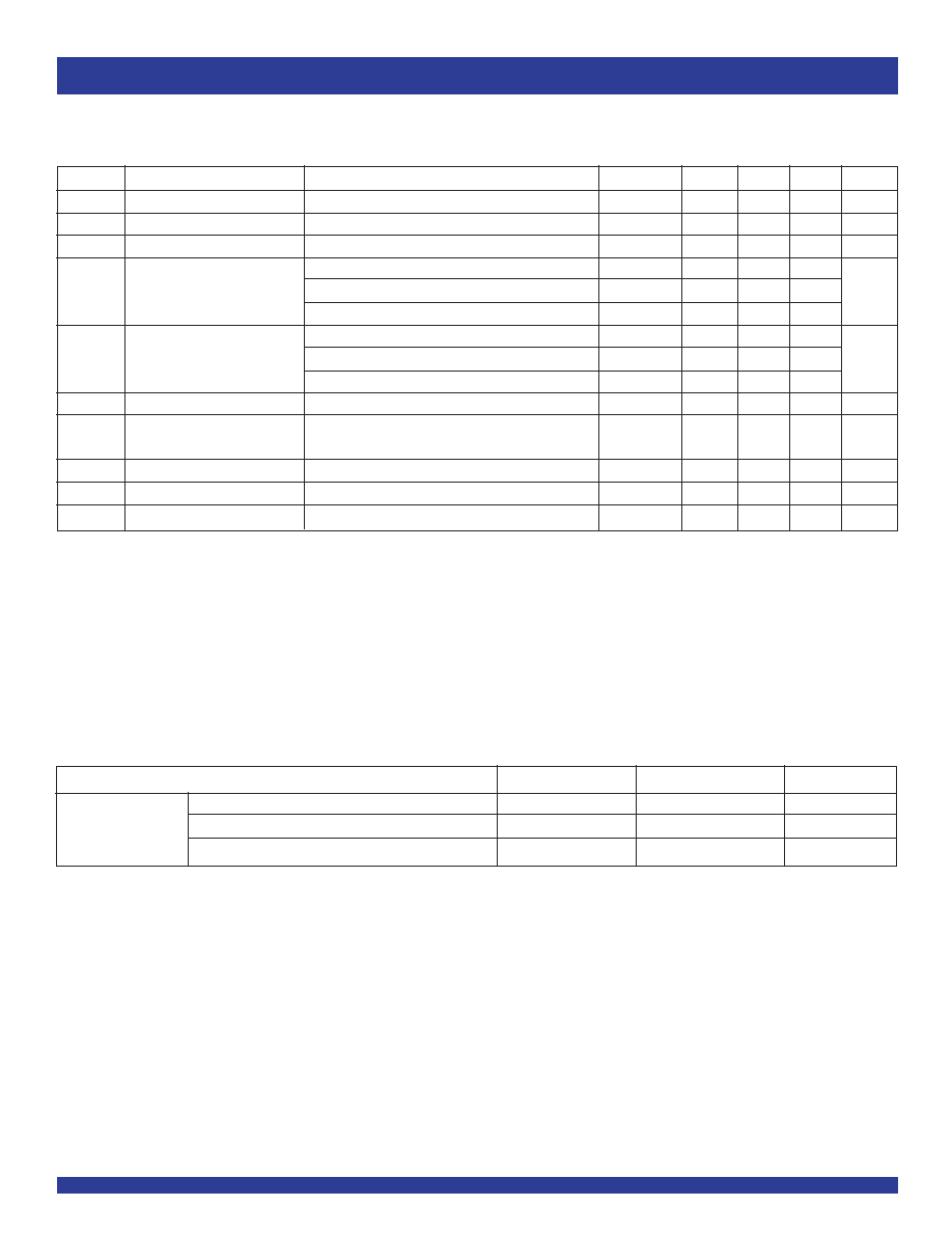
21
Y9
PLL
3
5
8
9
4
Y0
Y1
Y2
Y3
Y4
15
17
20
16
Y 5
Y6
Y7
Y8
24
13
23
AV
DD
FB IN
CLK
G
11
12
FBOUT
FUNCTIONAL BLOCK DIAGRAM
The IDT logo is a registered trademark of Integrated Device Technology, Inc.
FEATURES:
∑ Phase-Lock Loop Clock Distribution for Synchronous DRAM
Applications
∑ Distributes one clock input to one bank of ten outputs
∑ Output enable bank control
∑ External feedback (FBIN) pin is used to synchronize the
outputs to the clock input signal
∑ No external RC network required for PLL loop stability
∑ Operates at 3.3V V
DD
∑ tpd Phase Error at 133MHz: < ±150ps
∑ Jitter (peak-to-peak) at 133MHz: < ±75ps @ 133MHz
∑ Spread Spectrum Compatible
∑ Operating frequency 25MHz to 140MHz
∑ Available in 24-Pin TSSOP package
APPLICATIONS:
∑ SDRAM Modules
∑ PC Motherboards
∑ Workstations

2
0∫C TO 85∫C TEMPERATURE RANGE
IDTCSP2510C
3.3V PHASE-LOCK LOOP CLOCK DRIVER
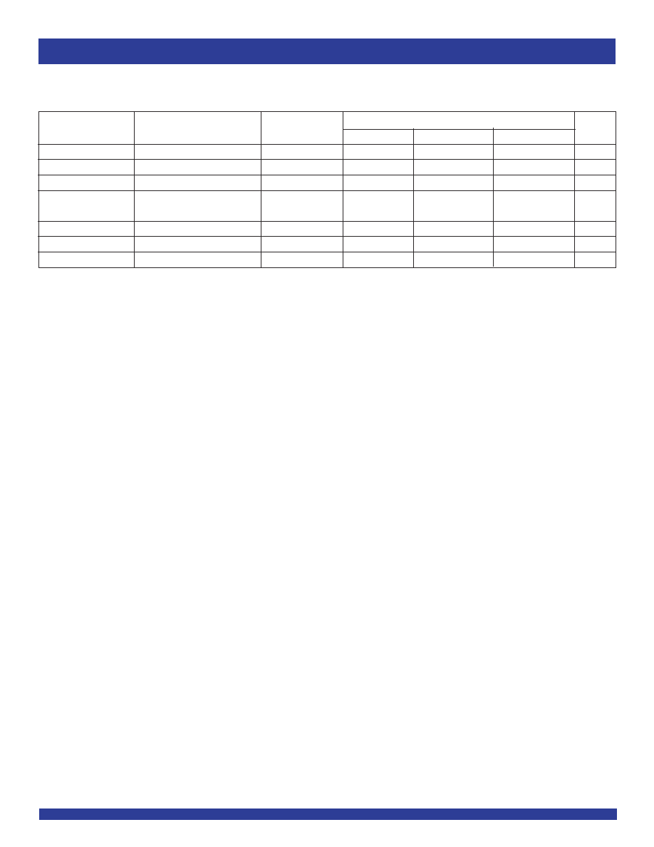
PIN CONFIGURATION
TSSOP
TOP VIEW
CLK
AV
DD
V
DD
Y9
Y8
GND
GND
Y7
Y6
Y5
V
DD
FBIN
AGND
V
DD
Y0
Y1
Y2
GND
GND
Y3
Y4
V
DD
G
FBOUT
24
23
22
21
20
19
18
17
16
15
14
13
1
2
3
4
5
6
7
8
9
10
11
12
ABSOLUTE MAXIMUM RATINGS
(1)
Symbol
Rating
Max
Unit
V
DD
Supply Voltage Range
≠0.5 to +4.6
V
V
I(1)
Input Voltage Range
≠0.5 to +6.5
V
V
O(1,2)
Voltage range applied to any
≠0.5 to V
DD
+ 0.5
V
output in the high or low state
I
IK
Input clamp current
≠50
mA
(V
I
<0)
I
OK
Terminal Voltage with Respect
±50
mA
(V
O
<0 or
to GND (inputs V
IH
2.5, V
IL
2.5)
V
O
> V
DD
)
I
O
Continuous Output Current
±50
mA
(V
O
= 0 to V
DD
)
V
DD
or GND
Continuous Current
±100
mA
T
STG
Storage Temperature Range
≠ 65 to +150
∞C
T
J
Junction Temperature
+150
∞C
NOTES:
1. Stresses greater than those listed under ABSOLUTE MAXIMUM RATINGS may cause
permanent damage to the device. This is a stress rating only and functional operation
of the device at these or any other conditions above those indicated in the operational
sections of this specification is not implied. Exposure to absolute maximum rating
conditions for extended periods may affect reliability.
2. The input and output negative-voltage ratings may be exceeded if the input and output
clamp-current ratings are observed.
3. The maximum package power dissipation is calculated using a junction temperature
of 150
∞
C and a board trace length of 750 mils.
CAPACITANCE
NOTE:
1. Unused inputs must be held HIGH or LOW to prevent them from floating.
Parameter
Description
Min.
Typ.
Max.
Unit
C
IN
Input Capacitance
5
pF
V
I
= V
DD
or GND
C
O
Output Capacitance
6
pF
V
O
= V
DD
or GND
C
L
Load Capacitance
30
pF
RECOMMENDED OPERATING CONDITIONS
Symbol
Description
Min.
Max.
Unit
V
DD
, AV
DD
Power Supply Voltage
3
3.6
V
T
A
Operating Free-Air Temperature
0
+85
∞
C

3
0∫C TO 85∫C TEMPERATURE RANGE
IDTCSP2510C
3.3V PHASE-LOCK LOOP CLOCK DRIVER
STATIC FUNCTION TABLE
(AV
DD
= 0V)
DYNAMIC FUNCTION TABLE
(AV
DD
= 3.3V)
PIN DESCRIPTION
Terminal
Name
No.
Type
Description
CLK
24
I
Clock input. CLK provides the clock signal to be distributed by the CSP2510C clock driver. CLK is used to provide the reference signal
to the integrated PLL that generates the clock output signals. CLK must have a fixed frequency and fixed phase for the PLL to obtain phase
lock. Once the circuit is powered up and a valid CLK signal is applied, a stabilization time is required for the PLL to phase lock the feedback
signal to its reference signal.
FBIN
13
I
Feedback input. FBIN provides the feedback signal to the internal PLL. FBIN must be hard-wired to FBOUT to complete the PLL. The
integrated PLL synchronizes CLK and FBIN so that there is nominally zero phase error between CLK and FBIN.
G
11
I
Output bank enable. G is the output enable for outputs Y(0:9). When G is low, outputs Y(0:9) are disabled to a logic-low state. When
G is high, all outputs Y(0:9) are enabled and switch at the same frequency as CLK.
FBOUT
12
O
Feedback output. FBOUT is dedicated for external feedback. It switches at the same frequency as CLK. When externally wired to
FBIN, FBOUT completes the feedback loop of the PLL.
Y (0:9)
3, 4, 5, 8, 9,
O
Clock outputs. These outputs provide low-skew copies of CLK. Output bank Y(0:9) is enabled via the G input. These outputs can be
15, 16, 17,
disabled to a logic-low state by de-asserting the G control input.
20, 21
AV
DD
23
Power
Analog power supply. AV
DD
provides the power reference for the analog circuitry. In addition, AV
DD
can be used to bypass the PLL
for test purposes. When AV
DD
is strapped to ground, PLL is bypassed and CLK is buffered directly to the device outputs.
AGND
1
Ground
Analog ground. AGND provides the ground reference for the analog circuitry.
V
DD
2, 10, 14, 22 Power
Power supply
GND
6, 7, 18, 19 Ground
Ground
Inputs
Outputs
G
CLK
Y (0:9)
FBOUT
L
L
L
L
L
H
L
H
H
H
H
H
H
L
L
L
H
running
running
running
Inputs
Outputs
G
CLK
Y (0:9)
FBOUT
X
L
L
L
L
running
L
running in
phase with CLK
L
H
L
H
H
running
running in
running in
phase with CLK
phase with CLK
H
H
H
H
4
0∫C TO 85∫C TEMPERATURE RANGE
IDTCSP2510C
3.3V PHASE-LOCK LOOP CLOCK DRIVER
DC ELECTRICAL CHARACTERISTICS OVER OPERATING FREE-AIR TEMPERA-
TURE RANGE
(1)
Symbol
Description
Test Conditions
V
DD
Min.
Typ.
(2)
Max.
Unit
V
IK
Input Clamp Voltage
I
I
= -18mA
3V
≠ 1.2
V
V
IH
Input HIGH Level
2
V
V
IL
Input LOW Level
0.8
V
I
OH
= -100
µA
Min. to Max. V
DD
≠ 0.2
V
OH
HIGH Level Output Voltage
I
OH
= -12mA
3V
2.1
V
I
OH
= -6mA
3V
2.4
I
OL
= 100
µA
Min. to Max.
0.2
V
OL
LOW Level Output Voltage
I
OL
= 12mA
3V
0.8
V
I
OL
= 6mA
3V
0.55
I
I
Input Current
V
I
= V
DD
or GND
3.6V
±5
µA
I
DD
Supply Current
V
I
= V
DD
or GND, AV
DD
= GND,
3.6V
10
µA
I
O
= 0, Outputs: LOW or HIGH
I
DD
Change in Supply Current
One input at V
DD
- 0.6V, other inputs at V
DD
or GND
3.3V to 3.6V
500
µA
C
PD
Power Dissipation Capacitance
3.6V
10
14
pF
I
DDA
(3)
AV
DD
Power Supply Current
AV
DD
= 3.3V
10
mA
NOTES:
1. For Industrial devices, operating free-air temperature = -40∞C to +85∞C.
2. For conditions shown as Min. or Max., use the appropriate value specified under recommended operating conditions.
3. For I
DD
of AV
DD
, see TYPICAL CHARACTERISTICS.
Min.
Max.
Unit
Clock frequency
25
140
MHz
f
CLOCK
Input clock duty cycle
40%
60%
Stabilization time
(2)
1
ms
TIMING REQUIREMENTS OVER OPERATING RANGE OF SUPPLY VOLTAGE AND
OPERATING FREE-AIR TEMPERATURE
(1)
NOTES:
1. For Industrial devices, operating free-air temperature = -40∞C to +85∞C.
2. Time required for the integrated PLL circuit to obtain phase lock of its feedback signal to its reference signal. For phase lock to be obtained, a fixed-frequency, fixed-phase
reference signal must be present at CLK. Until phase lock is obtained, the specifications for propagation delay, skew, and jitter parameters given in the switching characteristics
table are not applicable.
5
0∫C TO 85∫C TEMPERATURE RANGE
IDTCSP2510C
3.3V PHASE-LOCK LOOP CLOCK DRIVER
SWITCHING CHARACTERISTICS OVER OPERATING RANGE OF SUPPLY
VOLTAGE AND OPERATING FREE-AIR TEMPERATURE, C
L
= 30pF
(1)
V
DD
= 3.3V ± 0.3V
Parameter
(2)
From (Input)
To (Output)
Min.
Typ.
Max.
Unit
t
PHASE
error
100MHz < CLK
< 133MHz
FBIN
≠ 150
150
ps
t
PHASE
error ≠ jitter
(3)
CLK
= 133MHz
FBIN
≠ 50
50
ps
t
SK(o)
(4)
Any Y (133MHz)
Any Y
150
ps
Jitter (cycle-cycle)
CLK = 133MHz
Any Y or FBOUT
≠ 75
75
ps
(peak-to-peak)
Duty cycle reference
(5)
CLK = 133MHz
Any Y or FBOUT
45
55
%
t
R
Any Y or FBOUT
0.8
2.1
ns
t
F
Any Y or FBOUT
0.8
2.7
ns
NOTES:
1. For Industrial devices, operating free-air temperature = -40∞C to +85∞C. See PARAMETER MEASUREMENT INFORMATION.
2. The specifications for parameters in this table are applicable only after any appropriate stabilization time has elapsed.
3. Phase error does not include jitter.
4. The t
SK(O)
specification is only valid for equal loading of all outputs.
5. See TYPICAL CHARACTERISTICS.