 | –≠–ª–µ–∫—Ç—Ä–æ–Ω–Ω—ã–π –∫–æ–º–ø–æ–Ω–µ–Ω—Ç: QS316212 | –°–∫–∞—á–∞—Ç—å:  PDF PDF  ZIP ZIP |
1
IDTQS316212
HIGH-SPEED CMOS 24-BIT BUS-EXCHANGE SWITCH
INDUSTRIAL TEMPERATURE RANGE
NOVEMBER 1999
1999 Integrated Device Technology, Inc.
DSC-5569/1
c
INDUSTRIAL TEMPERATURE RANGE
FEATURES:
∑ Enhanced N channel FET with no inherent diode to Vcc
∑ Low propagation delay
∑ TTL-compatible input and output levels
∑ Undershoot clamp diodes on all switch and control inputs
∑ Available in SSOP and TSSOP packages
The IDT logo is a registered trademark of Integrated Device Technology, Inc.
APPLICATIONS:
∑ Resource sharing
∑ Crossbar switching
∑ Hot-docking
∑ Voltage translation (5V to 3.3V)
IDTQS316212
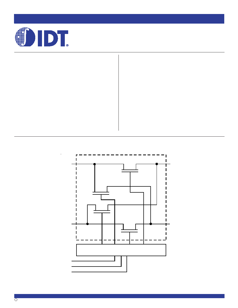
FUNCTIONAL BLOCK DIAGRAM
QUICKSWITCH
Æ
PRODUCTS
HIGH-SPEED CMOS
24-BIT BUS-EXCHANGE SWITCH
DESCRIPTION:
The QS316212 provides a set of 24 high-speed CMOS TTL-compatible
bus-exchange switches. The low ON resistance of the QS316212 allows
inputs to be connected to outputs without adding propagation delay and
without generating additional ground bounce noise. The device operates
as a 24-bit bus switch or a 12-bit bus exchanger, which provides data
exchanging between the four signal ports through the data-select (S0-S2)
terminals.
The QS316212 is characterized for operation at -40∞C to +85∞C.
1A1
1A2
1B2
1B1
S0
S1
S2
Flow Control
1 of 12 Chann els
2
INDUSTRIAL TEMPERATURE RANGE
IDTQS316212
HIGH-SPEED CMOS 24-BIT BUS-EXCHANGE SWITCH
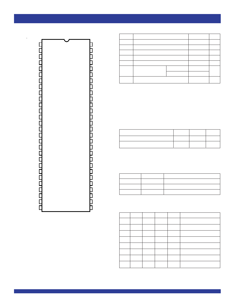
PIN CONFIGURATION
SSOP/ TSSOP
TOP VIEW
Pins
Typ.
Max.
(1)
Unit
Control Inputs
4
5
pF
Quickswitch Channels (Switch OFF)
7.5
9
pF
CAPACITANCE
(T
A
= +25∞C, f = 1MHz, V
IN
= 0V, V
OUT
= 0V)
NOTE:
1. This parameter is guaranteed but not production tested.
Pin Names
I/O
Description
1
Ax -
12
Ax
I/O
Bus A
1
Bx -
12
Bx
I/O
Bus B
S
0
- S
2
I
Data Select
PIN DESCRIPTION
Symbol
Description
Max
Unit
V
TERM
(2)
Supply Voltage to Ground
≠0.5 to +7
V
V
TERM
(3)
DC Switch Voltage V
S
≠0.5 to +7
V
V
TERM
(3)
DC Input Voltage V
IN
≠0.5 to +7
V
V
AC
AC Input Voltage (pulse width
20ns)
≠3
V
I
OUT
DC Output Current
120
mA
P
MAX
Maximum Power
SSOP
0.93
W
Dissipation (T
A
= 85∞C)
TSSOP
0.77
T
STG
Storage Temperature
≠65 to +150
∞C
ABSOLUTE MAXIMUM RATINGS
(1)
NOTES:
1. Stresses greater than those listed under ABSOLUTE MAXIMUM RATINGS may cause
permanent damage to the device. This is a stress rating only and functional operation
of the device at these or any other conditions above those indicated in the operational
sections of this specification is not implied. Exposure to absolute maximum rating
conditions for extended periods may affect reliability.
2. V
CC
terminals.
3. All terminals except V
CC
.
1
2
3
4
5
6
7
8
9
10
11
12
13
14
15
16
17
18
19
20
21
22
23
24
25
26
27
28
56
55
54
53
52
51
50
49
48
47
46
45
44
43
42
41
40
39
38
37
36
35
34
33
32
31
30
29
S0
1A1
1A2
2A1
2A2
3A1
3A2
GND
4A1
4A2
5A1
5A2
6A1
6A2
7A1
7A2
V
CC
8A1
GND
8A2
9A1
9A2
10A1
10A2
11A1
11A2
12A1
12A2
S1
S2
1B1
1B2
2B1
2B2
3B1
GND
3B2
4B1
4B2
5B1
5B2
6B1
6B2
7B1
7B2
8B1
GND
8B2
9B1
9B2
10B1
10B2
11B1
11B2
12B1
12B2
NOTE:
1. H = HIGH Voltage Level
L = LOW Voltage Level
Z = High-Impedance
S
2
S
1
S
0
xA
1
xA
2
Function
L
L
L
Z
Z
Disconnect
L
L
H
xB
1
Z
xA
1
to xB
1
L
H
L
xB
2
Z
xA
1
to xB
2
L
H
H
Z
xB
1
xA
2
to xB
1
H
L
L
Z
xB
2
xA
2
to xB
2
H
L
H
Z
Z
Disconnect
H
H
L
xB
1
xB
2
xA
1
to xB
1,
xA
2
to xB
2
H
H
H
xB
2
xB
1
xA
1
to xB
2,
xA
2
to xB
1
FUNCTION TABLE
(1)
3
IDTQS316212
HIGH-SPEED CMOS 24-BIT BUS-EXCHANGE SWITCH
INDUSTRIAL TEMPERATURE RANGE
Symbol
Parameter
Test Conditions
Min.
Typ.
(1)
Max.
Unit
V
IH
Input HIGH Voltage
Guaranteed Logic HIGH for Control Inputs
2
--
--
V
V
IL
Input LOW Voltage
Guaranteed Logic LOW for Control Inputs
--
--
0.8
V
I
IN
Input Leakage Current (Control Inputs)
0V
V
IN
V
CC
--
--
±1
µA
I
OZ
Off-State Current (Hi-Z)
0V
V
OUT
V
CC
, Switches OFF
--
--
±1
µA
R
ON
Switch ON Resistance
(2)
V
CC
= Min., V
IN
= 0V, I
ON
= 30mA
--
5
7
V
CC
= Min., V
IN
= 2.4V, I
ON
= 15mA
--
10
12
V
P
Pass Voltage
(3)
V
IN
= V
CC
= 5V, I
OUT
= -5
µA
3.7
4
4.2
V
DC ELECTRICAL CHARACTERISTICS OVER OPERATING RANGE
Following Conditions Apply Unless Otherwise Specified:
Industrial: T
A
= ≠40∞C to +85∞C, V
CC
= 5V ± 10%
NOTES:
1. Typical values are at V
CC
= 5V and T
A
= 25∞C.
2. R
ON
is guaranteed but not production tested.
3. Pass voltage is guaranteed but not production tested.
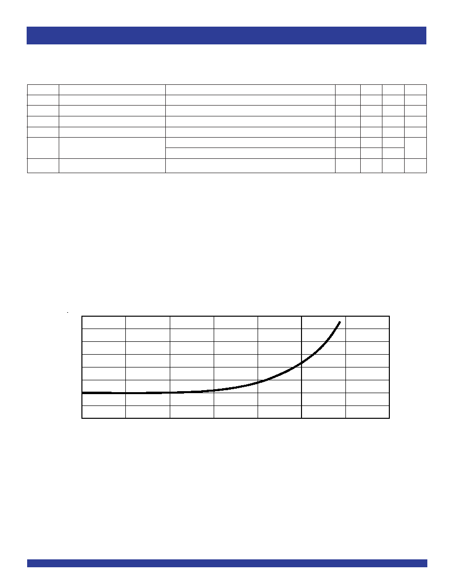
TYPICAL ON RESISTANCE vs V
IN
AT V
CC
= 5V
R
ON
(ohms)
V
IN
(Volts)
16
14
12
10
8
6
4
2
0
0.0
0.5
1.0
1.5
2.0
2.5
3.0
3.5
4
INDUSTRIAL TEMPERATURE RANGE
IDTQS316212
HIGH-SPEED CMOS 24-BIT BUS-EXCHANGE SWITCH
NOTES:
1. For conditions shown as Min. or Max., use the appropriate values specified under DC Electrical Characteristics.
2. Per TTL-driven input (V
IN
= 3.4V). A and B pins do not contribute to
Icc.
3. This current applies to the control inputs only and represents the current required to switch internal capacitance at the specified frequency. The A and B inputs generate no significant
AC or DC currents as they transition. This parameter is guaranteed but not production tested.
POWER SUPPLY CHARACTERISTICS
Symbol
Parameter
Test Conditions
(1)
Max.
Unit
I
CCQ
Quiescent Power Supply Current
V
CC
= Max., V
IN
= GND or V
CC
, f = 0
3
µA
I
CC
Power Supply Current per Control Input HIGH
(2)
V
CC
= Max., V
IN
= 3.4V, f = 0
2.5
mA
I
CCD
Dynamic Power Supply Current per MHz
(3)
V
CC
= Max., A and B Pins Open, Control Inputs Toggling @ 50% Duty Cycle
0.25
mA/MHz
SWITCHING CHARACTERISTICS OVER OPERATING RANGE
T
A
= -40∞C to +85∞C, V
CC
= 5V ± 10%
C
LOAD
= 50pF, R
LOAD
= 500
unless otherwise noted.
Symbol
Parameter
Min
.
(1)
Typ.
Max.
Unit
t
PLH
Data Propagation Delay
(2)
0.25
(3)
ns
t
PHL
xAx to xBx, xBx to xAx
t
PZL
Switch Turn-On Delay
1.5
6.5
ns
t
PZH
Sx to xAx, xBx
t
PLZ
Switch Turn-Off Delay
(2)
1.5
6.2
ns
t
PHZ
Sx to xAx, xBx
NOTES:
1. Minimums are guaranteed but not production tested.
2. This parameter is guaranteed but not production tested.
3. The bus switch contributes no propagation delay other than the RC delay of the ON resistance of the switch and the load capacitance. The time constant for the switch alone
is of the order of 0.25ns at C
L
= 50pF. Since this time constant is much smaller than the rise and fall times of typical driving signals, it adds very little propagation delay to the
system. Propagation delay of the bus switch, when used in a system, is determined by the driving circuit on the driving side of the switch and its interaction with the load on
the driven side.
5
IDTQS316212
HIGH-SPEED CMOS 24-BIT BUS-EXCHANGE SWITCH
INDUSTRIAL TEMPERATURE RANGE
ORDERING INFORMATION
CORPORATE HEADQUARTERS
for SALES:
for Tech Support:
2975 Stender Way
800-345-7015 or 408-727-6116
logichelp@idt.com
Santa Clara, CA 95054
fax: 408-492-8674
(408) 654-6459
www.idt.com
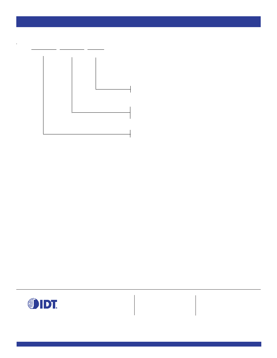
IDTQS
XXXXX
XX
Package
Device Type
Blank
Industrial (-40∞C to +85∞C)
Shrink Small Outline Package
Thin Shrink Small Outline Package
PV
PA
316212
High Speed CMOS 24-Bit Bus-Exchange Switch
X
Process