 | –≠–ª–µ–∫—Ç—Ä–æ–Ω–Ω—ã–π –∫–æ–º–ø–æ–Ω–µ–Ω—Ç: QS3B491 | –°–∫–∞—á–∞—Ç—å:  PDF PDF  ZIP ZIP |
FEATURES/BENEFITS
∑ Fully configurable Switch Matrix
∑ Sub-nanosecond Propagation Delay
∑ User-friendly Individual Port Control
∑ Power-on Reset
∑ Synchronous/Asynchronous Configuration Control
∑ Programmable Active Terminators on each Port
∑ Resistor options for line termination
∑ Available in 64-pin TQFP package
DESCRIPTION
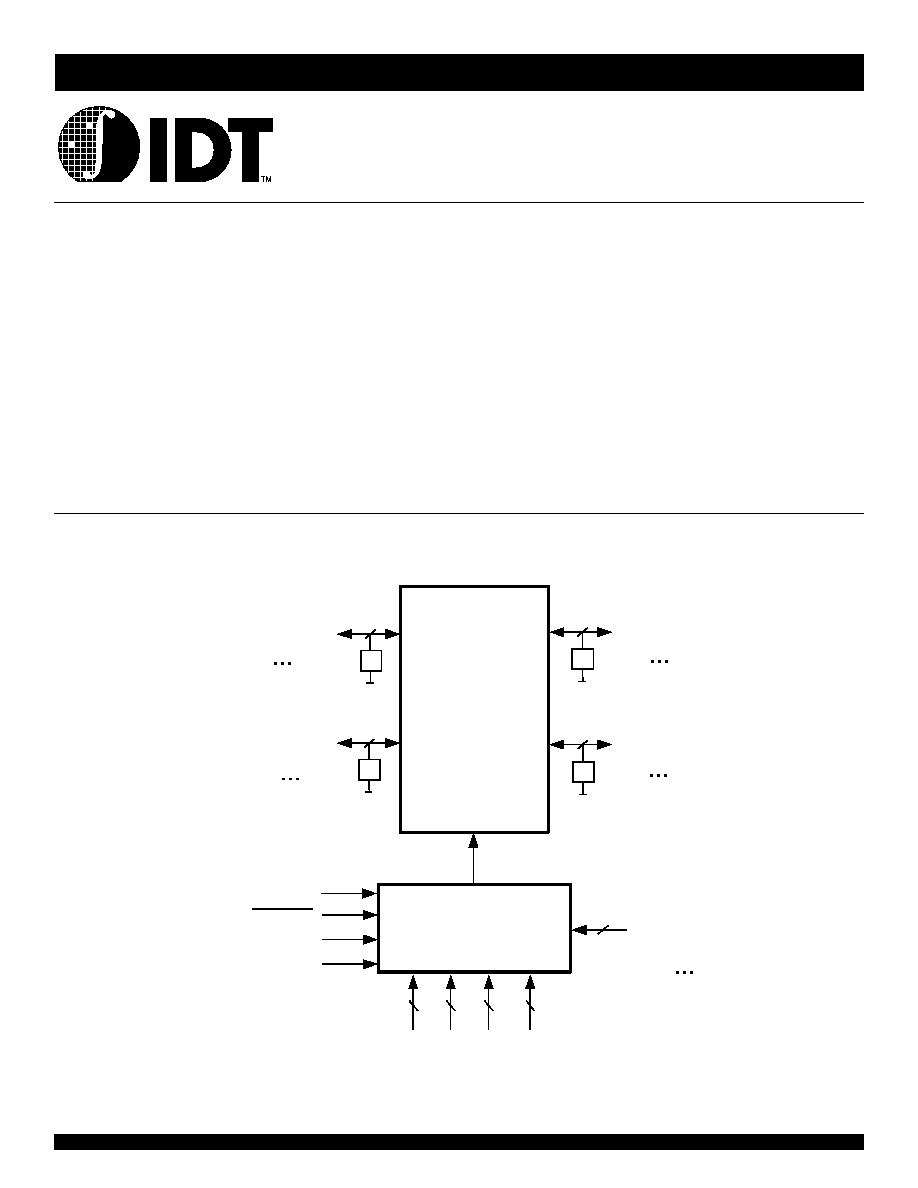
The QS3B491 and QS3B2491 are high speed Crossbar switches
organized as four independent 9-bit wide ports using QSI's 0.5micron
CMOS technology. The switch matrix consists of N-channel FET switches
controlled by the configuration logic. When closed, the switches permit
bidirectional data flow with near-zero propagation delay. The N-channel
FETs also facilitate 5V to 3.3V, and 5V to 2.5V voltage translation between
ports.
The switch matrix can be configured for independent connection be-
tween any two ports as well as for multi-port broadcasting. Configuration
control is either synchronous or asynchronous. In the synchronous mode,
the control logic behaves like a Register. New configuration is stored on the
positive edge of the Clock (CLK) if Clock Enable (
CLKEN) is at logic LOW.
JULY 1999
1
©
1999 Integrated Device Technology, Inc
DSC-XXXXXX
QS3B491
QS3B2491
ADVANCE
INFORMATION
QUICKSWITCH
Æ
PRODUCTS
HIGH-SPEED CMOS
CLOCKED 4 PORT X 9-BIT
CROSSBAR SWITCHTM
FUNCTIONAL BLOCK DIAGRAM
S W ITC H
M A TR IX
T
9
T
9
C P ort
(C
0
C
8
)
D P ort
(D
0
D
8
)
A Port
(A
0
A
8
)
B Port
(B
0
B
8
)
C O N F IG U R AT IO N
C O N TR O L LO G IC
4
T
9
T
9
OE
CL KE N
CL K
LE
2
2
2
2
S
A
S
B
S
C
S
D
T
CA
T
CD
2
©
1999 Integrated Device Technology, Inc
IDT
QS3B491 AND QS3B2491
DSC-XXXXXX
In the Asynchronous mode, switch configuration logic behaves as a
Transparent Latch under the control of LE signal. When LE is HIGH, the
Latch is in the transparent mode. When LE is LOW, the configuration
that meets the set-up time requirements is latched. An internal Power-
ON Reset circuir disables all switches during power supply ramp-up and
ramp-down.
Two port selection inputs are provided for port-independent intercon-
nect control. Each port can be independently configured as a source or
destination. This control scheme eliminates `illegal' control input com-
binations.
Each I/O has a programmable Terminator with three modes of operation:
OFF, Active Terminator (Last Value Latch), and Passive (Resistive)
Terminator. Terminators for each port are connected to independent
VBIAS pins (V
BA
...V
BD
)and are controlled by independent Terminator
Control (TCx) pins with three-state inputs. This control arrangement
provides maximum flexibility for voltage translation between ports.
The QS3B491 is a low resistance Crossbar Switch, with ON resistance
of 9
typical. The QS32491 adds an internal series resistor and is ideal for
series termination of PCB traces and for the reduction of signal overshoots
and undershoots.
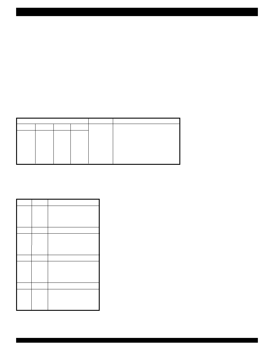
Control Inputs
Mode Status
X
X
X
L
-
All Switches OFF
X
X
H
H
Asynch
Transparent Mode
H
X
L
H
Synch
Hold Previous Configuration
L
L
H
Synch
Load Configuration
L
H
L
H
Asynch
Hold Previous Configuration
L
L
L
H
Asynch
Hold Previous Configuration
CLKEN
CLK LE OE
CONFIGURATION CONTROL
S1A
S0A
A - Port Status
L
L
Source
L
H
Destination (B -> A)
H
L
Destination (C -> A)
H
H
Destination (D -> A)
PORT SELECTION CONTROL
S1D
S0D
D - Port Status
L
L
Destination (A -> D)
L
H
Destination (B -> D)
H
L
Destination (C -> D)
H
H
Source
S1C
S0C
C - Port Status
L
L
Destination (A -> C)
L
H
Destination (B -> C)
H
L
Source
H
H
Destination (D -> C)
S1B
S0B
B - Port Status
L
L
Destination (A -> B)
L
H
Source
H
L
Destination (C -> B)
H
H
Destination (D -> B)
©
1999 Integrated Device Technology, Inc
IDT
QS3B491 AND QS3B2491
DSC-XXXXXX
3
TCA, TCB, TCC, TCD
Terminator Status
H
Active Terminator (Bus Hold) to V
BIAS
(V
BA
...V
BD
)
L
Resistor Termination to V
BIAS
(V
BA
...V
BD
)
Terminator OFF
TERMINATOR CONTROL
OPEN
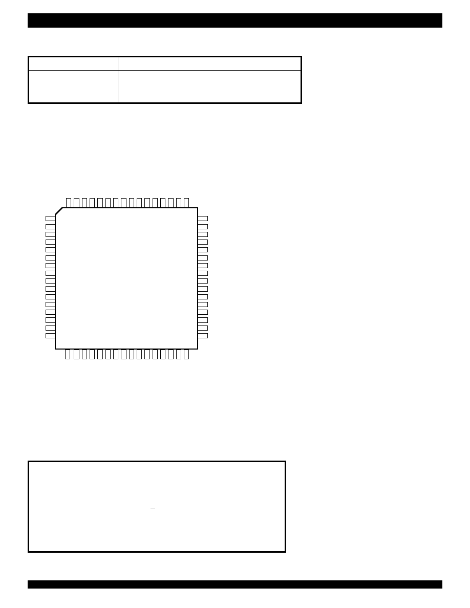
PIN CONFIGURATION
(ALL PINS TOP VIEW)
TQFP
Note: ABSOLUTE MAXIMUM CONTINU-
OUS RATINGS are those values beyond
which damage to the device may occur.
Exposure to these conditions or conditions
beyond those indicated rating may adversely
affect device reliability. Functional operation
under absolute-maximum conditions is not
implied.
Supply Voltage to Ground .......................................................................... ≠0.5V to 7.0V
Bias Voltage to Ground .............................................................................. ≠0.5V to 7.0V
DC Switch Input Voltage ............................................................................ ≠0.5V to 7.0V
DC Control Input Voltage ........................................................................... ≠0.5V to 7.0V
AC Control Input Voltage (for pulse width
<
20ns ................................................... ≠3.0V
DC Input Diode Current, V
IN
< 0 ........................................................................... ≠20mA
DC I/O Current, Max. Sink Current Per Pin .......................................................... 100mA
Maximum Power Dissipation .............................................................................. 1.0 watt
Storage Temperature Range .................................................................. ≠65
o
C to 150
o
C
ABSOLUTE MAXIMUM RATINGS
1
V
BA
D2
D1
D0
C2
V
CC
C1
C0
B2
B1
B0
A2
A1
A0
T
CA
GND
V
BD
A6
A7
A8
B6
V
CC
B7
B8
C6
C7
C8
D6
D7
D8
T
CD
GND
V
BB
A
3
A
4
A
5
B
3
GND
B
4
B
5
C
3
C
4
V
CC
C
5
D
3
D
4
D
5
V
BC
T
CB
LE
CLK
CLKEN
OE
S
0A
S
1A
V
CC
GND
S
0B
S
1B
S
0C
S
1C
S
0D
S
1D
T
CC
2
3
4
5
6
7
8
9
10
11
12
13
14
15
16
48
47
46
45
44
43
42
41
40
39
38
37
36
35
34
33
64
63
62
61
60
59
58
57
56
55
54
53
52
51
50
49
17
18
19
20
21
22
23
24
25
26
27
28
29
30
31
32

4
©
1999 Integrated Device Technology, Inc
IDT
QS3B491 AND QS3B2491
DSC-XXXXXX
Symbol
Parameter
Test Conditions
(1)
Max
Unit
I
CCQ
Quiescent Power
V
IN
= GND or V
CC
, f = 0
600
µ A
Supply Current
V
BIAS
= 5.5V
I
CC
Power Supply Current
(2)
V
IN
= 3.4V, f = 0
2.5
mA
per Input HIGH
per Control Input
Q
CCD
Dynamic Power Supply
V
CC
= V
BIAS
= 5.5V, Switching Pins Open
mA/
Current per MHz
(3)
Control Inputs Toggling @ 50% Duty Cycle
MHz
Pins
64-Pin TQFP
Units
Typ
Max
Control Inputs
5
7
pF
I/O (Switches OFF)
12
15
pF
I/O (One-to-one Channels)
25
30
pF
CAPACITANCE
T
A
= 25
o
C, f = 1MHz, V
IN
= 0V, V
OUT
= 0V
Note: Capacitance is characterized but not tested.
TYPICAL ON RESISTANCE VS V
IN
AT 5.0 V
CC
, T
A
= 25∞C (3B491)
Note: For QS3B2491 add 25
to the adove values.
POWER SUPPLY CHARACTERISTICS
Notes:
1. For conditions shown as Min. or Max., use the appropriate values specified under DC specifications.
2. Per TTL driven input (V
IN
= 3.4V, control inputs only). A and B pins do not contribute to
I
CC
.
3. This current applies to the control inputs only and represents the current required to switch internal capacitance at the specified frequency.
4. This parameter is guaranteed but not production tested.
16
14
12
10
8
6
4
2
0
R
ON
(ohms)
0.0
0.5
1.0
1.5
2.0
2.5
3.0
3.5
V
IN
(Volts)
©
1999 Integrated Device Technology, Inc
IDT
QS3B491 AND QS3B2491
DSC-XXXXXX
5
Symbol
Parameter
Test Conditions
Min
Typ
(1)
Max
Unit
A. CONTROL INPUTS
V
IH
Input HIGH Voltage
Guaranteed Logic HIGH
2.0
--
--
V
for Control Pins, except T
CA
...T
CD
V
IL
Input LOW Voltage
Guaranteed Logic LOW
--
--
0.8
V
for Control Pins, except T
CA
...T
CD
V
IHH
Input HIGH Voltage
3-Level Inputs Only
V
CC
--
--
V
T
CA
...T
CD
≠1.0
V
IMM
Input MID Voltage
3-Level Inputs Only
V
CC
/2
--
V
CC
/2
V
T
CA
...T
CD
≠0.5
+0.5
V
ILL
Input LOW Voltage
3-Level Inputs Only
--
--
1.0
V
T
CA
...T
CD
|I
IN
|
Input Leakage Current
0V
V
IN
V
CC
--
0.02
1
µA
for Control Inputs, except T
CA
...T
CD
V
IC
Input Clamp Voltage
I
IN
= ≠18mA, V
CC
= 4.5V
--
--
≠1.2
V
B. Switch I/O (A, B, C & D Ports)
| I
OZ
|
Off-State Current (Hi-Z)
0V
V
IN
V
CC
--
0.02
1
µA
R
ON
Switch On Resistance
Vcc = Min., V
IN
= 0.0V, 3B491
--
8
10
I
ON
= 30mA 3B2491
--
25
40
V
CC
= Min., V
IN
= 2.4V, 3B491
--
12
15
I
ON
= 15mA 3B2491
--
30
45
I
BHL
Input Hold Current
(2,3)
V
CC
= V
BIAS
= 4.50V V
IN
= 0.8V
75
--
--
µA
I
BHH
(A or B Port)
Switch OFF V
IN
= 2.0V
≠75
--
--
T
CA
...T
CD
= HIGH
| I
BH
|
Input Current
(4)
V
CC
= V
BIAS
= 5.5V
V
IN
= 0, or V
CC
--
--
50
µ A
A,B Port
Switch OFF
0.8V< V
IN
<2.0V
--
--
650
(5)
T
CA
...T
CD
= HIGH
V
P
Pass Voltage
(5)
V
IN
= V
CC
= 5V, I
OUT
= ≠5µA
3.7
4.0
4.2
V
I
IL
Input Current
V
CC
= V
BIAS
= 4.5V V
IN
= 0V
--
≠1
--
mA
Switch OFF, T
CA
...T
CD
= LOW
DC ELECTRICAL CHARACTERISTICS OVER OPERATING RANGE
T
A
= ≠40
o
C to 85
o
C, V
CC
= 5.0V ± 10%
Notes:
1. Typical values indicate V
CC
= 5.0V and T
A
= 25∞C.
2. I
BHL
- Minimum sustaining "sink" current at the input for V
IN
= 0.8V. Signifies the logic LOW latching capability.
3. I
BHH
- Minimum sustaining "source" current at the input for V
IN
= 2.0V. Signifies the logic HIGH latching capability.
4. | I
BH
| Magnitude of the input current specified under two conditions:
(a) Input voltage at GND or V
CC
. This indicates the input current under steady-state condition.
(b) Input voltage between 0.8V and 2.0V (TTL input threshold range). This indicates the maximum input current during transient condition. The driver connected to the input
must overcome this current requirement in order to switch the logic state of the Bus-hold circuit.
5. Pass voltage is guaranteed, but not production tested.

6
©
1999 Integrated Device Technology, Inc
IDT
QS3B491 AND QS3B2491
DSC-XXXXXX
Symbol
Description
Min
Typ
Max
Units
t
PLH
Single Channel Port-Port Propagation
--
0.5
ns
t
PHL
Delay (3B491)
t
PLH
Single Channel Port-Port Propagation
--
1.5
ns
t
PHL
Delay (3B2491)
t
PZL
Asynchronous Enable to Switch
1.5
--
6.5
ns
t
PZH
Turn-on Delay
t
PLZ
Asynchronous Enable to Switch
1.5
--
5.5
ns
t
PHZ
Turn-off Delay
t
PZL
Select Control to Switch Turn-on Delay
1.5
--
6.5
ns
t
PZH
(Asynchronous Mode)
t
PLZ
Select Control to Switch Turn-off Delay
1.5
--
5.5
ns
t
PHZ
(Asynchronous Mode)
t
PZL
CLK to Switch Turn-on Delay
1.5
--
6.5
ns
t
PZH
(Synchronous Mode)
t
PLZ
CLK to Switch Turn-off Delay
1.5
--
5.5
ns
t
PHZ
(Synchronous Mode)
t
SCS
Select Control Input to CLK Set-up Time
3
--
ns
t
HCS
Select Control Input to CLK Hold Time
0
--
ns
t
SEC
CLKEN to CLK Set-up Time
3
--
ns
t
HEC
CLKEN to CLK Hold Time
0
--
ns
t
SCL
Select Control Input to LE Set-up Time
3
--
ns
t
HCL
Select Control Input to LE Hold Time
0
--
ns
t
W
Clock Pulse Width (HIGH)
4
--
ns
SWITCHING CHARACTERISTICS OVER OPERATING RANGE
T
A
= ≠40
o
C to 85
o
C, V
CC
= 5.0V +10%
C
LOAD
= 30pF, R
LOAD
= 500
unless otherwise noted
CORPORATE HEADQUARTERS
for SALES:
2975 Stender Way
800-345-7015 or 408-727-6116
Santa Clara, CA 95054
fax: 408-492-8674
www.idt.com*
*To search for sales office near you, please click the sales button found on our home page or dial the 800# above and press 2.
The IDT logo is a registered trademark of Integrated Device Technology, Inc.