 | –≠–ª–µ–∫—Ç—Ä–æ–Ω–Ω—ã–π –∫–æ–º–ø–æ–Ω–µ–Ω—Ç: QS3V245 | –°–∫–∞—á–∞—Ç—å:  PDF PDF  ZIP ZIP |
1
INDUSTRIAL TEMPERATURE RANGE
IDTQS3V245
3.3V HIGH SPEED BUS SWITCH
2000 Integrated Device Technology, Inc.
DSC-5512/1
c
IDTQS3V245
INDUSTRIAL TEMPERATURE RANGE
QUICKSWITCH
Æ
PRODUCTS
3.3V HIGH SPEED BUS SWITCH
The IDT logo is a registered trademark of Integrated Device Technology, Inc.
APPLICATIONS:
∑ 3.3V to 2.5V voltage translation
∑ 2.5V to 1.8V voltage translation
∑ PCI bus isolation hot swap
FEATURES:
∑ 5
bi-directional switches connect inputs to outputs
∑ Pin compatibility with QS3245
∑ 250ps propagation delay
∑ Undershoot Clamp Diodes on all switch and control Inputs
∑ LVTTL-compatible control Inputs
∑ Available in SOIC and QSOP packages
NOVEMBER 2000
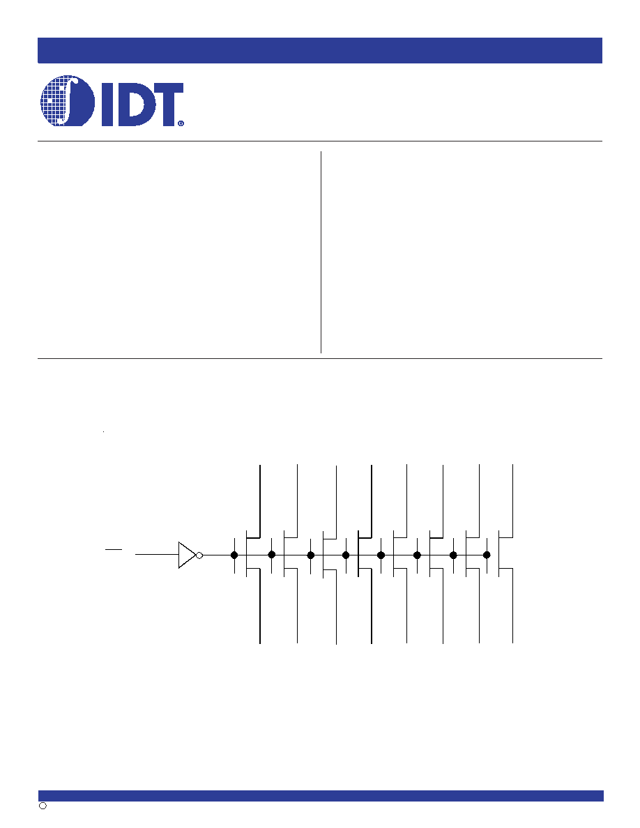
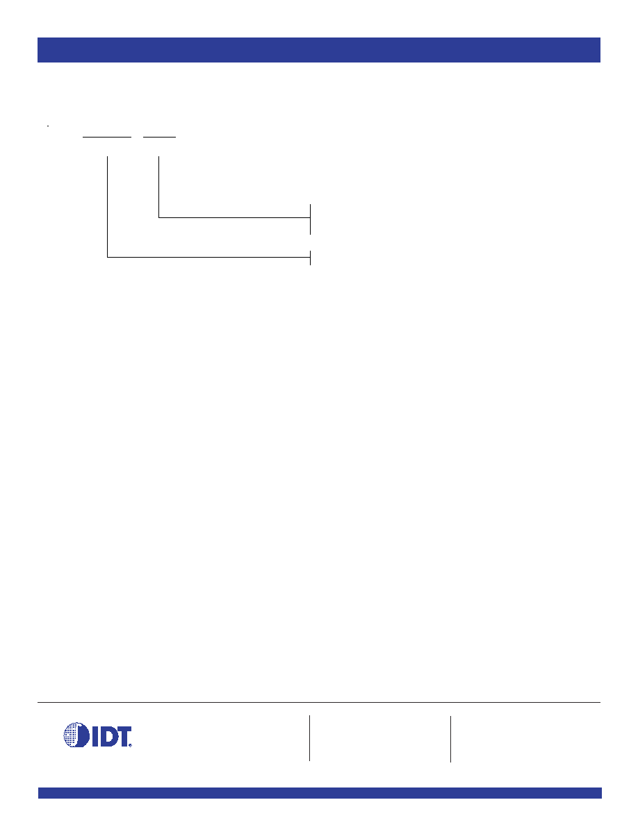
FUNCTIONAL BLOCK DIAGRAM
DESCRIPTION:
The QS3V245 is an 8-bit high speed bus switch controlled by LVTTL-
compatible active low enable signal. When closed, the switches exhibit near
zero propagation delay without generating additional ground bounce or
switching noise.
The QS3V245 is specially designed for direct interface between 3.3V and
2.5V devices without any external components. When operating from a 3.3V
supply, the logic high level at the switch output is clamped to 2.5V when the
switch input signal exceeds 2.5V. This device can be used for switching 2.5V
buses without signal attenuation. The ON resistance at 3.3V V
CC
is less than
5
typical, providing near zero propagation delay through the switch.
Absence of DC path from switch I/O pins to V
CC
or ground makes QS3V245
an ideal device for hot swapping applications.
The QS3V245 is characterized for operation from -40
∞C to +85∞C.
OE
A0
B0
A1
B1
A2
B2
A3
B3
A4
B4
A5
B5
A6
B6
A7
B7
19
2
3
4
5
6
7
8
9
18
17
16
15
14
13
12
11
2
INDUSTRIAL TEMPERATURE RANGE
IDTQS3V245
3.3V HIGH SPEED BUS SWITCH
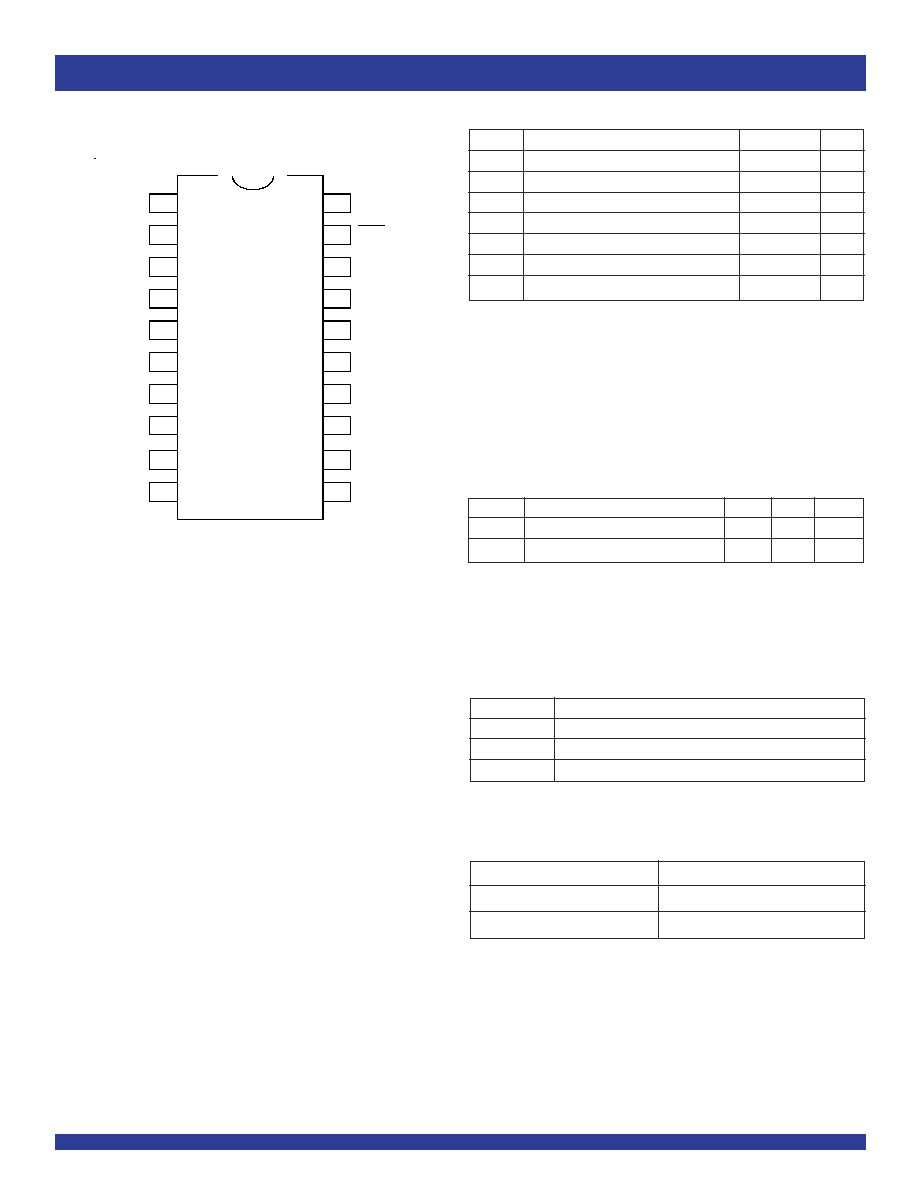
PIN CONFIGURATION
Symbol
Description
Max
Unit
V
TERM
(2)
Supply Voltage to Ground
≠0.5 to +4.6
V
V
S
DC Switch Voltage
≠0.5 to +4.6
V
V
IN
DC Input Voltage
≠0.5 to +4.6
V
V
AC
AC Input Voltage (pulse width
20ns)
≠3
V
I
OUT
DC Output Current (max. sink current/pin)
120
mA
Maximum Power Dissipation
0.5
W
T
STG
Storage Temperature
≠65 to +150
∞C
ABSOLUTE MAXIMUM RATINGS
(1)
Symbol
Parameter
(1)
Typ.
Max.
Unit
C
IN
Control Inputs
4
6
pF
C
I/O
Quickswitch Channels (Switch OFF)
5
7
pF
CAPACITANCE
(T
A
= +25∞C, f = 1MHz, V
IN
= 0V, V
OUT
= 0V)
NOTE:
1. As applicable to the device type.
Pin Names
Description
OE
Output Enable
A x
Data I/Os
B x
Data I/Os
PIN DESCRIPTION
NOTE:
1. H = HIGH Voltage Level
L = LOW Voltage Level
OE
Outputs
H
Disconnected
L
Ax = Bx
FUNCTION TABLE
(1)
SOIC/ QSOP
TOP VIEW
NOTES:
1. Stresses greater than those listed under ABSOLUTE MAXIMUM RATINGS may cause
permanent damage to the device. This is a stress rating only and functional operation
of the device at these or any other conditions above those indicated in the operational
sections of this specification is not implied. Exposure to absolute maximum rating
conditions for extended periods may affect reliability.
2. V
CC
terminals.
NC
A0
A2
A3
A7
A6
GND
2
3
4
5
6
7
8
9
10
11
12
15
14
13
16
17
18
19
20
1
A1
A4
A5
OE
B1
V
CC
B6
B5
B7
B0
B3
B4
B2
3
INDUSTRIAL TEMPERATURE RANGE
IDTQS3V245
3.3V HIGH SPEED BUS SWITCH
TYPICAL ON RESISTANCE vs V
IN
AT V
CC
= 3.3V
R
ON
(ohms)
V
IN
(Volts)
Symbol
Parameter
Test Conditions
Min.
Typ.
(1)
Max.
Unit
V
IH
Input HIGH Voltage
Guaranteed Logic HIGH for Control Inputs
2
--
--
V
V
IL
Input LOW Voltage
Guaranteed Logic LOW for Control Inputs
--
--
0.8
V
I
IN
Input Leakage Current (Control Inputs)
0V
V
IN
V
CC
--
--
1
µA
I
OZ
Off-State Current (Hi-Z)
0V
V
OUT
V
CC
, Switches OFF
--
0.001
1
µA
V
CC
= Min., V
IN
= 0V, I
ON
= 8mA
--
5
7
R
ON
Switch ON Resistance
V
CC
= Min., V
IN
= 1.7V, I
ON
= 8mA
--
15
20
V
CC
= 2.3V, V
IN
= 0V, I
ON
= 8mA
--
7
--
V
CC
= 2.3V, V
IN
= 1.3V, I
ON
= 8mA
--
25
--
V
P
Pass Voltage
(2)
V
IN
= V
CC
= 3.3V, I
OUT
= -5µA
2.3
2.7
2.9
V
V
IN
= V
CC
= 2.5V, I
OUT
= -5µA
--
1.8
--
DC ELECTRICAL CHARACTERISTICS OVER OPERATING RANGE
Following Conditions Apply Unless Otherwise Specified:
Industrial: T
A
= ≠40∞C to +85∞C, V
CC
= 3.3V ±0.3V
NOTES:
1. Typical values are at V
CC
= 3.3V and T
A
= 25∞C.
2. Pass voltage is guaranteed, but not production tested.
14
0.5
1
1.5
2
2.5
12
10
8
6
4
2
0
0
16
4
INDUSTRIAL TEMPERATURE RANGE
IDTQS3V245
3.3V HIGH SPEED BUS SWITCH
NOTES:
1. For conditions shown as Min. or Max., use the appropriate values specified under DC Electrical Characteristics.
2. Per TTL driven input (V
IN
= 3V, control inputs only). A and B pins do not contribute to Icc.
3. This current applies to the control inputs only and represents the current required to switch internal capacitance at the specified frequency. The A and B inputs generate no significant
AC or DC currents as they transition. This parameter is guaranteed but not production tested.
POWER SUPPLY CHARACTERISTICS
T
A
= ≠40∞C to +85∞C, V
CC
= 3.3V ±0.3V
Symbol
Parameter
Test Conditions
(1)
Min.
Max.
Unit
I
CCQ
Quiescent Power Supply Current
V
CC
= Max., V
IN
= GND or V
CC
, f = 0
--
3
µA
I
CC
Power Supply Current
(2)
per Input HIGH
V
CC
= Max., V
IN
= 3V or V
CC
, f = 0 per Control Input
--
30
µA
I
CCD
Dynamic Power Supply Current per MHz
(3)
V
CC
= 3.3V, A and B Pins Open, Control Input Toggling
--
0.15
mA/MHz
@ 50% Duty Cycle
SWITCHING CHARACTERISTICS OVER OPERATING RANGE
(1)
T
A
= -40∞C to +85∞C
Symbol
Parameter
Min.
Typ
.
Max.
Unit
t
PLH
Data Propagation Delay
(2,3)
0.25
ns
t
PHL
Ax to/from Bx
t
PZL
Switch Turn-On Delay
0.5
6.5
ns
t
PZH
OE to Ax/Bx
t
PLZ
Switch Turn-Off Delay
(2)
0.5
4
ns
t
PHZ
OE to Ax/Bx
NOTES:
1. See TEST CIRCUITS AND WAVEFORMS. Minimums guaranteed but not production tested
2. This parameter is guaranteed but not production tested.
3. The bus switch contributes no propagation delay other than the RC delay of the ON resistance of the switch and the load capacitance. The time constant for the switch alone
is of the order of 0.25ns for C
L
= 30pF. Since this time constant is much smaller than the rise and fall times of typical driving signals, it adds very little propagation delay to the
system. Propagation delay of the bus switch, when used in a system, is determined by the driving circuit on the driving side of the switch and its interaction with the load on
the driven side.
5
INDUSTRIAL TEMPERATURE RANGE
IDTQS3V245
3.3V HIGH SPEED BUS SWITCH
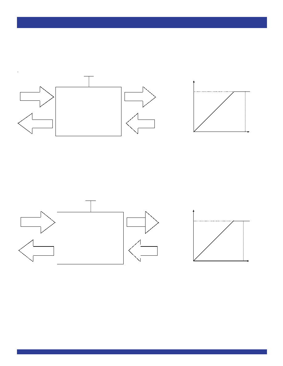
OUTPUT VI CHARACTERISTICS
Outputs Low Characteristic
Outputs High Characteristic
PASS VOLTAGE vs V
CC
250
200
150
100
50
0
0
0.5
1
1.5
2
V
OUT
(Volts)
I
O
s
-
(
m
A
)
-250
-200
-150
-100
-50
1
2
3
4
V
OUT
(Volts)
I
O
s
-
(
m
A
)
-300
3
2.5
2
1.5
2.2
2.4
2.7
3
3.3
3.6
V
CC
(V)
V
O
U
T
-
(
V
o
l
t
s
)
V
OU T
= 2.5V @ V
C C
= 3.3V
V
O UT
= 1.8V @ V
C C
= 2.5V
6
INDUSTRIAL TEMPERATURE RANGE
IDTQS3V245
3.3V HIGH SPEED BUS SWITCH
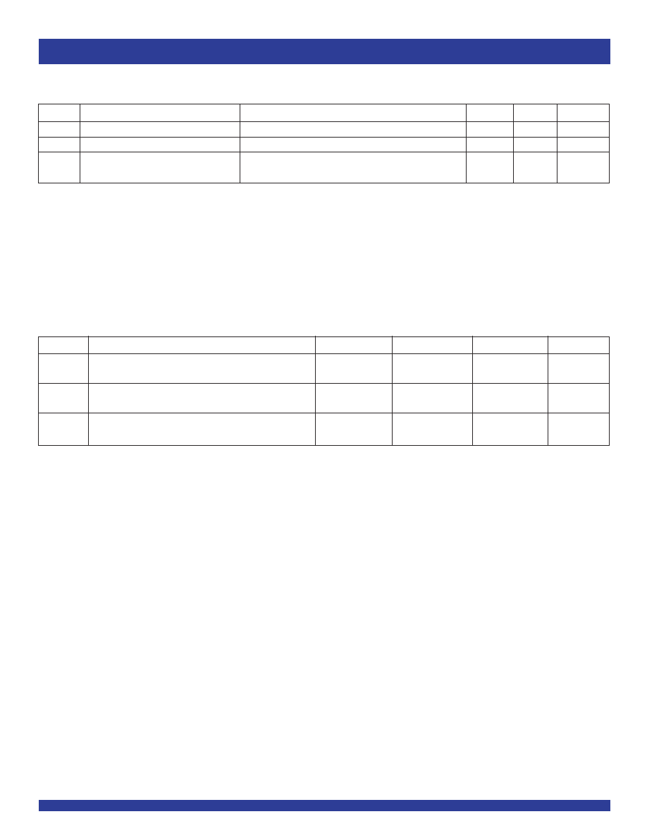
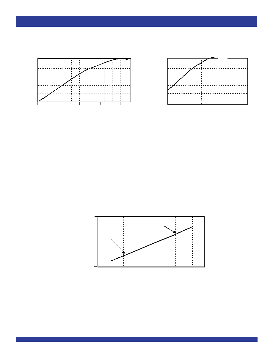
QS3V245
2.5V
2.5V
3.3V
2.5V
3.3V
QS3V245
1.8V
1.8V
2.5V
1.8V
2.5V
V
IN
2.5V
V
OUT
3.3V Supply
0V
3.3V
O
u
t
put
of
Sw
i
t
c
h
Input of Sw itch
V
IN
1.8V
V
O UT
2.5V S upply
0V
2.5V
Ou
t
p
u
t o
f
S
w
it
ch
Input of S witch
2.5V TO 1.8V VOLTAGE TRANSLATION
3.3V TO 2.5V VOLTAGE TRANSLATION
7
INDUSTRIAL TEMPERATURE RANGE
IDTQS3V245
3.3V HIGH SPEED BUS SWITCH
ORDERING INFORMATION
CORPORATE HEADQUARTERS
for SALES:
for Tech Support:
2975 Stender Way
800-345-7015 or 408-727-6116
logichelp@idt.com
Santa Clara, CA 95054
fax: 408-492-8674
(408) 654-6459
www.idt.com
IDTQS
XXXXX
XX
Package
Device Type
3V245
3.3V High Speed Bus Switch
SO
Q
Small Outline IC (Gull Wing)
Quarter Size Small Outline Package