1
INDUSTRIAL TEMPERATURE RANGE
IDTQS3VH16244
2.5V / 3.3V 16-BIT HIGH BANDWIDTH BUS SWITCH
MARCH 2002
2001 Integrated Device Technology, Inc.
DSC-5877/3
c
INDUSTRIAL TEMPERATURE RANGE
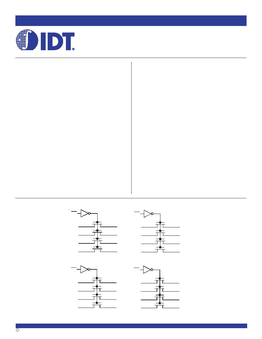
FUNCTIONAL BLOCK DIAGRAM
DESCRIPTION:
The QS3VH16244 HotSwitch is a 16-bit high band bus switch. The
QS3VH16244 has very low ON resistance, resulting in under 250ps propa-
gation delay through the switch. The switches can be turned ON under the
control of the LVTTL-compatible xG signal for bidirectional data flow with no
added delay or ground bounce. In the OFF and ON states, the switches are
5V-tolerant. In the OFF state, the switches offer very high impedance at the
terminals.
The combination of near-zero propagation delay, high OFF impedance, and
over-voltage tolerance makes the QS3VH16244 ideal for high performance
communications applications.
The QS3VH16244 is characterized for operation from -40
∞C to +85∞C.
The IDT logo is a registered trademark of Integrated Device Technology, Inc.
FEATURES:
∑ N channel FET switches with no parasitic diode to Vcc
--
--
- Isolation under power-off conditions
--
--
- No DC path to Vcc or GND
--
--
- 5V tolerant in OFF and ON state
∑ 5V tolerant I/Os
∑ Low R
ON
- 4
typical
∑ Flat R
ON
characteristics over operating range
∑ Rail-to-rail switching 0 - 5V
∑ Bidirectional dataflow with near-zero delay: no added ground
bounce
∑ Excellent R
ON
matching between channels
∑ Vcc operation: 2.3V to 3.6V
∑ High bandwidth - up to 500 MHz
∑ LVTTL-compatible control Inputs
∑ Undershoot Clamp Diodes on all switch and control Inputs
∑ Low I/O capacitance, 4pF typical
∑ Available in SSOP and TSSOP packages
APPLICATIONS:
∑ Hot-swapping
∑ 10/100 Base-T, Ethernet LAN switch
∑ Low distortion analog switch
∑ Replaces mechanical relay
∑ ATM 25/155 switching
IDTQS3VH16244
PRELIMINARY
QUICKSWITCH
Æ
PRODUCTS
2.5V / 3.3V 16-BIT HIGH
BANDWIDTH BUS SWITCH
1G
1
Y
1
1
Y
2
1
Y
3
1
Y
4
1
A
1
1
A
2
1
A
3
1
A
4
2G
2
Y
1
2
Y
2
2
Y
3
2
Y
4
2
A
1
2
A
2
2
A
3
2
A
4
3 G
3
Y
1
3
Y
2
3
Y
3
3
Y
4
3
A
1
3
A
2
3
A
3
3
A
4
4 G
4
Y
1
4
Y
2
4
Y
3
4
Y
4
4
A
1
4
A
2
4
A
3
4
A
4
2
INDUSTRIAL TEMPERATURE RANGE
IDTQS3VH16244
2.5V / 3.3V 16-BIT HIGH BANDWIDTH BUS SWITCH
ABSOLUTE MAXIMUM RATINGS
(1)
Symbol
Description
Max.
Unit
V
TERM(2)
Supply Voltage to Ground
≠ 0.5 to 4.6
V
V
TERM(3)
DC Switch Voltage V
S
≠ 0.5 to 5.5
V
V
TERM(3)
DC Input Voltage V
IN
≠ 0.5 to 5.5
V
V
AC
AC Input Voltage (pulse width
20ns)
≠ 3
V
I
OUT
DC Output Current (max. current/pin)
120
mA
T
STG
Storage Temperature
-65 to +150
∞
C
NOTES:
1. Stresses greater than those listed under ABSOLUTE MAXIMUM RATINGS may
cause permanent damage to the device. This is a stress rating only and functional
operation of the device at these or any other conditions above those indicated in the
operational sections of this specification is not implied. Exposure to absolute
maximum rating conditions for extended periods may affect reliability.
2. V
CC
terminals.
3. All terminals except V
CC
.
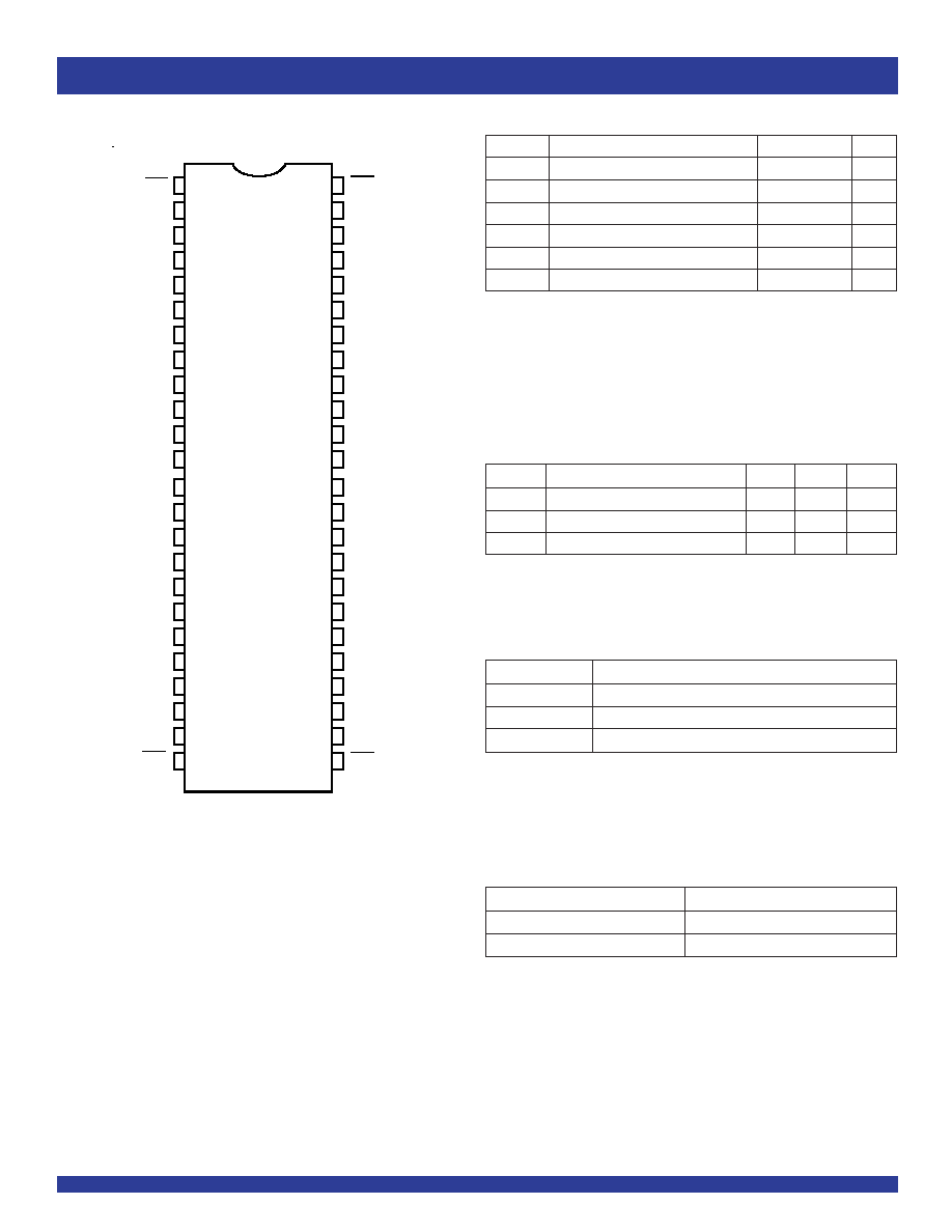
PIN CONFIGURATION
SSOP/ TSSOP
TOP VIEW
CAPACITANCE
(T
A
= +25
o
C, f = 1MHz, V
IN
= 0V, V
OUT
= 0V)
Symbol
Parameter
(1)
Typ.
Max.
Unit
C
IN
Control Inputs
3
5
pF
C
I/O
Quickswitch Channels (Switch OFF)
4
6
pF
C
I/O
Quickswitch Channels (Switch ON)
8
12
pF
NOTE:
1. This parameter is guaranteed but not production tested.
PIN DESCRIPTION
Pin Names
Description
xG
Output Enable
xAx
Data I/Os
xYx
Data I/Os
FUNCTION TABLE
(1)
xG
Outputs
H
Disconnected
L
xAx = xYx
NOTE:
1. H = HIGH Voltage Level
L = LOW Voltage Level
48
1G
2G
1
47
1
A
1
2
1
Y
1
46
3
1
Y
2
1
A
2
45
4
GND
GND
44
5
1
Y
3
1
A
3
43
6
1
Y
4
1
A
4
41
8
2
Y
1
2
A
1
40
9
2
Y
2
2
A
2
39
10
GND
GND
42
7
V
CC
V
CC
38
11
2
Y
3
2
A
3
37
2
Y
4
12
2
A
4
36
3
Y
1
3
A
1
13
35
3
A
2
14
3
Y
2
34
15
GND
GND
33
16
3
Y
3
3
A
3
32
17
3
Y
4
3
A
4
31
18
V
CC
V
CC
29
20
4
Y
2
4
A
2
28
21
GND
GND
27
22
4
Y
3
4
A
3
30
19
4
Y
1
4
A
1
26
23
4
Y
4
4
A
4
25
4G
24
3G

3
INDUSTRIAL TEMPERATURE RANGE
IDTQS3VH16244
2.5V / 3.3V 16-BIT HIGH BANDWIDTH BUS SWITCH
DC ELECTRICAL CHARACTERISTICS OVER OPERATING RANGE
Following Conditions Apply Unless Otherwise Specified:
Industrial: T
A
= ≠40∞C to +85∞C, V
CC
= 3.3V ± 0.3V
Symbol
Parameter
Test Conditions
Min.
Typ.
(1)
Max.
Unit
V
IH
Input HIGH Voltage
Guaranteed Logic HIGH
V
CC
= 2.3V to 2.7V
1.7
--
--
V
for Control Inputs
V
CC
= 2.7V to 3.6V
2
--
--
V
IL
Input LOW Voltage
Guaranteed Logic HIGH
V
CC
= 2.3V to 2.7V
--
--
0.7
V
for Control Inputs
V
CC
= 2.7V to 3.6V
--
--
0.8
I
IN
Input Leakage Current (Control Inputs)
0V
V
IN
V
CC
--
--
±1
µA
I
OZ
Off-State Current (Hi-Z)
0V
V
OUT
5V, Switches OFF
--
--
±1
µA
I
OFF
Data Input/Output Power Off Leakage
V
IN
or V
OUT
0V to 5V, V
CC
= 0V
--
--
±1
µA
V
CC
= 2.3V
V
IN
= 0V
I
ON
= 30mA
--
6
8
R
ON
Switch ON Resistance
(Typ. at V
CC
= 2.5V) V
IN
= 1.7V
I
ON
= 15mA
--
7
9
V
CC
= 3V
V
IN
= 0V
I
ON
= 30mA
--
4
6
V
IN
= 2.4V
I
ON
= 15mA
--
5
8
NOTE:
1. Typical values are at V
CC
= 3.3V and T
A
= 25∞C, unless otherwise noted.
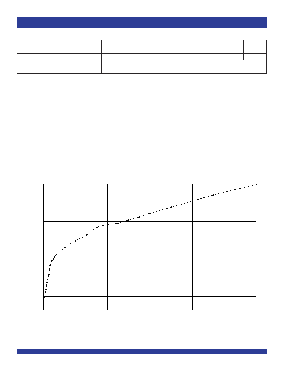
TYPICAL ON RESISTANCE vs V
IN
AT V
CC
= 3.3V
R
ON
(ohms)
V
IN
(Volts)
16
14
12
10
8
6
4
2
0
0.0
0.5
1.0
1.5
2.0
2.5
3.0
3.5
4.0
5.0
4.5
4
INDUSTRIAL TEMPERATURE RANGE
IDTQS3VH16244
2.5V / 3.3V 16-BIT HIGH BANDWIDTH BUS SWITCH
POWER SUPPLY CHARACTERISTICS
Symbol
Parameter
Test Conditions
(1)
Min.
Typ.
Max.
Unit
I
CCQ
Quiescent Power Supply Current
V
CC
= Max., V
IN
= GND or V
CC
, f = 0
--
1.5
3
mA
I
CC
Power Supply Current
(2,3)
per Input HIGH
V
CC
= Max., V
IN
= 3V, f = 0 per Control Input
--
--
30
µA
I
CCD
Dynamic Power Supply Current
(4)
V
CC
= 3.3V, A and Y Pins Open, Control Inputs
See Typical I
CCD
vs Enable Frequency graph below
Toggling @ 50% Duty Cycle
NOTES:
1. For conditions shown as Min. or Max., use the appropriate values specified under DC Electrical Characteristics.
2. Per input driven at the specified level. A and Y pins do not contribute to
Icc.
3. This parameter is guaranteed but not tested.
4. This parameter represents the current required to switch internal capacitance at the specified frequency. The A and Y inputs do not contribute to the Dynamic Power Supply
Current. This parameter is guaranteed but not production tested.
TYPICAL I
CCD
vs ENABLE FREQUENCY CURVE AT V
CC
= 3.3V
I
CCD
(mA)
ENABLE FREQUENCY (MHZ)
0
2
4
6
8
10
12
14
16
18
20
0
2
4
6
8
10
12
14
16
18
20
5
INDUSTRIAL TEMPERATURE RANGE
IDTQS3VH16244
2.5V / 3.3V 16-BIT HIGH BANDWIDTH BUS SWITCH
SWITCHING CHARACTERISTICS OVER OPERATING RANGE
T
A
= -40∞C to +85∞C
V
CC
= 2.5 ± 0.2V
(1)
V
CC
= 3.3 ± 0.3V
(1)
Symbol
Parameter
Min
.
(4)
Max.
Min
.
(4)
Max.
Unit
t
PLH
Data Propagation Delay
(2,3)
0.2
0.2
ns
t
PHL
xAx to/from xYx
t
PZH
Switch Turn-On Delay
1.5
8
1.5
8
ns
t
PZL
xG to xAx/xYx
t
PHZ
Switch Turn-Off Delay
1.5
7.5
1.5
7.5
ns
t
PLZ
xG to xAx/xYx
f
xG
Operating Frequency - xG
(2,5)
10
20
MHz
NOTES:
1. See Test Conditions under TEST CIRCUITS AND WAVEFORMS.
2. This parameter is guaranteed but not production tested.
3. The bus switch contributes no propagation delay other than the RC delay of the ON resistance of the switch and the load capacitance. The time constant for the switch alone
is of the order of 0.2ns at C
L
= 50pF. Since this time constant is much smaller than the rise and fall times of typical driving signals, it adds very little propagation delay to the
system. Propagation delay of the bus switch, when used in a system, is determined by the driving circuit on the driving side of the switch and its interaction with the load on
the driven side.
4. Minimums are guaranteed but not production tested.
5. Maximum toggle frequency for xG control input (pass voltage > V
CC
, V
IN
= 5V, R
LOAD
> 1M
, no C
LOAD
).

6
INDUSTRIAL TEMPERATURE RANGE
IDTQS3VH16244
2.5V / 3.3V 16-BIT HIGH BANDWIDTH BUS SWITCH
PHY
3VH
SWITCH
4.5V
PP
LOGIC
SIDE
Z = 100
10Mbps to 100Mbps
2V
PP
4.5V
PP
LOGIC
SIDE
Z = 100
TWISTED PAIR
>100m
CHARGE PUMP
OE
Vcc = 3.3V
0 to +5V
NFET
+6.5V
DRIVER
0 to +5V
SINGLE HOT
SWITCH
CARD I/O
ON CARD
LOGIC
CON
N
E
C
T
O
R
QS3
V
HX
XX
CPU
RAM
BUS
CARD I/O
ON CARD
LOGIC
CON
N
E
C
T
O
R
QS
3
V
HXX
X
PLUGGABLE CARD/ LIVE SYSTEM
ZERO DOWN TIME SYSTEM
Rail-to-Rail Switching
SOME APPLICATIONS FOR HOTSWITCH PRODUCTS
Fast Ethernet Data Switching (LAN Switch)
Hot Swapping
7
INDUSTRIAL TEMPERATURE RANGE
IDTQS3VH16244
2.5V / 3.3V 16-BIT HIGH BANDWIDTH BUS SWITCH
Open
V
LOAD
GN D
V
CC
Pulse
G enerator
D .U .T.
500
500
C
L
R
T
V
IN
V
OUT
(1, 2)
SAM E PH AS E
IN PUT TR AN SITION
OPPOSITE PHASE
IN PU T TRAN SITIO N
0V
0V
V
OH
V
OL
t
PLH
t
PH L
t
PHL
t
PLH
OU TPUT
V
IH
V
T
V
T
V
IH
V
T
CON TR OL
INPU T
t
PLZ
0V
OU TPU T
N OR M ALLY
LOW
t
PZ H
0V
S W ITCH
CLO SE D
OU TPU T
NO RM ALLY
HIGH
EN ABLE
D ISABLE
SW ITCH
O P E N
t
PH Z
0V
V
O L +
V
LZ
V
O H
V
T
V
T
t
PZL
V
LO AD/2
V
L O A D /2
V
IH
V
T
V
O L
V
O H -
V
H Z
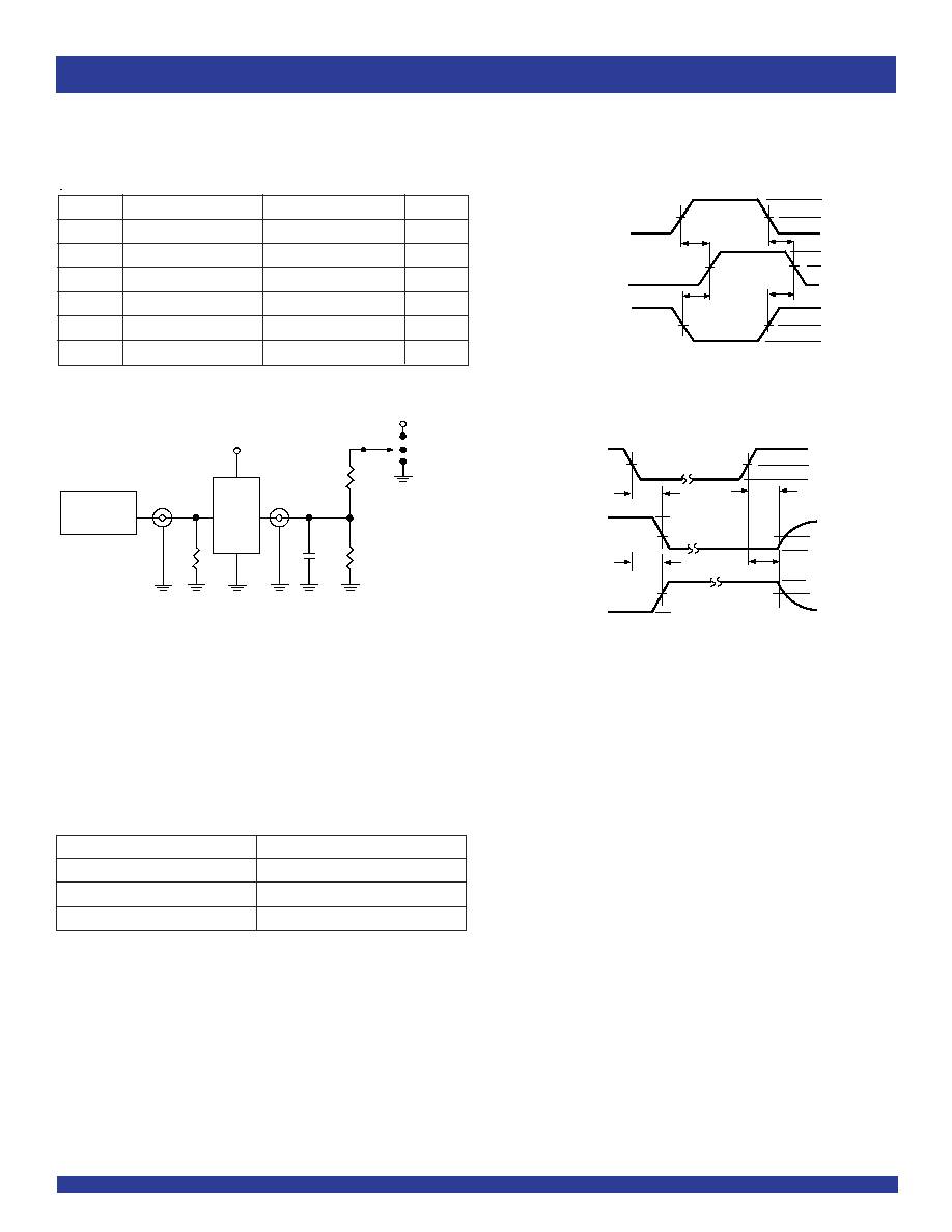
TEST CIRCUITS AND WAVEFORMS
Enable and Disable Times
NOTE:
1. Diagram shown for input Control Enable-LOW and input Control Disable-HIGH.
Propagation Delay
Test Circuits for All Outputs
DEFINITIONS:
C
L
= Load capacitance: includes jig and probe capacitance.
R
T
= Termination resistance: should be equal to Z
OUT
of the Pulse Generator.
NOTES:
1. Pulse Generator for All Pulses: Rate
1.0MHz; t
F
2.5ns; t
R
2.5ns.
2. Pulse Generator for All Pulses: Rate
1.0MHz; t
F
2ns; t
R
2ns.
SWITCH POSITION
Test
Switch
t
PLZ
/
t
PZL
V
LOAD
t
PHZ/
t
PZH
GND
t
PD
Open
TEST CONDITIONS
Symbol
V
CC
(1)
= 3.3V ± 0.3V
V
CC
(2)
= 2.5V ± 0.2V
Unit
V
LOAD
6
2 x Vcc
V
V
IH
3
Vcc
V
V
T
1.5
V
CC
/2
V
V
LZ
300
150
mV
V
HZ
300
150
mV
C
L
50
30
pF
8
INDUSTRIAL TEMPERATURE RANGE
IDTQS3VH16244
2.5V / 3.3V 16-BIT HIGH BANDWIDTH BUS SWITCH
ORDERING INFORMATION
CORPORATE HEADQUARTERS
for SALES:
for Tech Support:
2975 Stender Way
800-345-7015 or 408-727-6116
logichelp@idt.com
Santa Clara, CA 95054
fax: 408-492-8674
(408) 654-6459
www.idt.com
IDTQS
XXXXX
XX
Package
Device Type
3VH16244
2.5V / 3.3V 16-Bit High Bandwidth Bus Switch
PV
PA
Shrink Small Outline IC
Thin Shrink Small Outline Package