1
INDUSTRIAL TEMPERATURE RANGE
QS5919T
LOW SKEW TTL PLL CLOCK DRIVER WITH INTEGRATED LOOP FILTER
R
D
Q
Q
0
R
D
Q
Q
1
R
D
Q
Q
2
R
D
Q
Q
3
R
D
Q
Q
4
R
D
Q
Q
5
R
D
Q
Q /2
Q
O E/R ST
0
1
1
0
/2
V C O
LO O P
FIL TER
PH A S E
D ETEC TO R
1
0
FR EQ _SEL
REF_SEL
LO C K
FEE D BACK
SYNC
0
SYNC
1
PLL_E N
2xQ
PE
SEPTEMBER 2000
2000 Integrated Device Technology, Inc.
DSC-5815/-
c
QS5919T
INDUSTRIAL TEMPERATURE RANGE
LOW SKEW TTL PLL
CLOCK DRIVER WITH
INTEGRATED LOOP FILTER
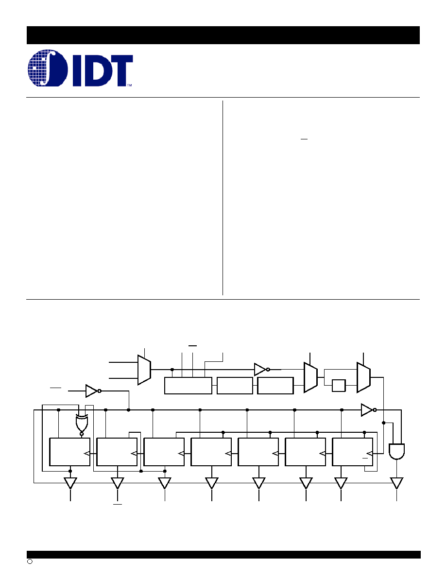
FUNCTIONAL BLOCK DIAGRAM
DESCRIPTION
The QS5919T Clock Driver uses an internal phase locked loop (PLL)
to lock low skew outputs to one of two reference clock inputs. Eight outputs
are available: 2xQ, Q
0
-Q
4
, Q
5
, Q/2. Careful layout and design ensure <
350ps skew between the Q
0
-Q
4
, and Q/2 outputs. The QS5919T includes
an internal RC filter which provides excellent jitter characteristics and
eliminates the need for external components. Various combinations of
feedback and a divide-by-2 in the VCO path allow applications to be
customized for linear VCO operation over a wide range of input SYNC
frequencies. The PLL can also be disabled by the PLL_EN signal to allow
low frequency or DC testing. The LOCK output asserts to indicate when
phase lock has been achieved. The QS5919T is designed for use in high-
performance workstations, multi-board computers, networking hardware,
and mainframe systems. Several can be used in parallel or scattered
throughout a system for guaranteed low skew, system-wide clock distribu-
tion networks.
For more information on PLL clock driver products, see Application Note
AN-227.
FEATURES:
�
5V operation
�
Low noise TTL level outputs
�
< 350ps output skew, Q
0
�Q
4
�
2xQ output, Q outputs, Q output, Q/2 output
�
Outputs 3-state and reset while OE/RST low
�
PLL disable feature for low frequency testing
�
Internal loop filter RC network
�
Functional equivalent to Motorola MC88915
�
Positive or negative edge synchronization (PE)
�
Balanced drive outputs �24mA
�
160MHz maximum frequency (2xQ output)
�
Available in QSOP and PLCC packages
2
INDUSTRIAL TEMPERATURE RANGE
QS5919T
LOW SKEW TTL PLL CLOCK DRIVER WITH INTEGRATED LOOP FILTER
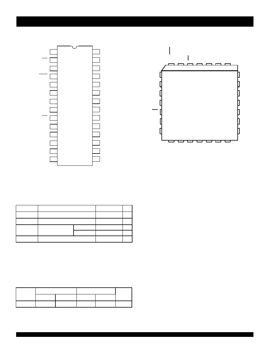
PIN CONFIGURATION
QSOP
TOP VIEW
PLCC
TOP VIEW
ABSOLUTE MAXIMUM RATINGS
(1)
Symbol
Rating
Max.
Unit
V
DD
, AV
DD
Supply Voltage to Ground
�0.5 to +7
V
V
IN
DC Input Voltage V
IN
�0.5 to +7
V
Maximum Power
QSOP
655
mW
Dissipation (T
A
= 85�C)
PLCC
770
mW
T
STG
Storage Temperature Range
�65�C to +150�C
�C
NOTE:
1. Stresses greater than those listed under ABSOLUTE MAXIMUM
RATINGS may cause permanent damage to the device. This is a
stress rating only and functional operation of the device at these or
any other conditions above those indicated in the operational sections
of this specification is not implied. Exposure to absolute maximum
rating conditions for extended periods may affect reliability.
CAPACITANCE
(T
A
= 25
�
C, f = 1MHz, V
IN
= 0V)
QSOP
PLCC
Parameter
Typ.
Max.
Typ.
Max.
Unit
C
IN
3
4
4
6
pF
20
19
18
15
16
23
22
24
21
17
V
D D
GND
PLL_EN
GND
Q/2
Q
3
LOCK
V
D D
2xQ
Q
1
25
28
27
26
V
D D
Q
2
GND
Q
4
SO28-9
2
3
1
9
10
AV
D D
PE
OE/RST
SYNC
0
FEEDBACK
AGND
5
6
7
4
8
Q
5
11
12
FREQ_SEL
SYNC
1
GND
V
D D
REF_SEL
13
14
Q
0
GND
OE
/
R
S
T
V
DD
Q
5
GN
D
Q
4
V
DD
2x
Q
Q/2
GND
Q
3
V
D D
Q
2
GND
LOCK
P
LL_
E
N
GN
D
Q
1
V
DD
Q
0
GN
D
FR
EQ
_
S
EL
FEED BAC K
REF_SEL
SYN C
0
AV
D D
PE
AGND
SYN C
1
28
4
3
2
1
27
26
25
24
23
22
21
20
19
5
6
7
8
9
10
11
12
13
14
15
16
17
18
J28-1
3
INDUSTRIAL TEMPERATURE RANGE
QS5919T
LOW SKEW TTL PLL CLOCK DRIVER WITH INTEGRATED LOOP FILTER
PIN DESCRIPTION
Pin Name
I/O
Description
SYNC
0
I
Reference clock input
SYNC
1
I
Reference clock input
REF_SEL
I
Reference clock select. When 1, selects SYNC
1
. When 0, selects SYNC
0
.
FREQ_SEL
I
VCO frequency select. For choosing optimal VCO operating frequency depending on input frequency.
FEEDBACK
I
PLL feedback input which is connected to a user selected output pin. External feedback provides flexibility for different output
frequency relationships. See the Frequency Selection Table for more information.
Q
0
-Q
4
O
Clock outputs
Q
5
O
Clock output. Matched in frequency, but inverted with respect to Q.
2xQ
O
Clock output. Matched in phase, but frequency is double the Q frequency.
Q/2
O
Clock output. Matched in phase, but frequency is half the Q frequency.
LOCK
O
PLL lock indication signal. 1 indicates positive lock. 0 indicates that the PLL is not locked and outputs may not be synchronized to
the inputs.
OE/
RST
I
Output enable/asynchronous reset. Resets all output registers. When 0, all outputs are held in a tri-stated condition. When 1,
outputs are enabled.
PLL_EN
I
PLL enable. Enables and disables the PLL. Useful for testing purposes.
PE
I
When
PE is LOW, outputs are synchronized with the positive edge of SYNC. When HIGH, outputs are synchronized with the
negative edge of SYNC.
V
DD
--
Power supply for output buffers.
AV
DD
--
Power supply for phase lock loop and other internal circuitries.
GND
--
Ground supply for output buffers.
AGND
--
Ground supply for phase lock loop and other internal circuitries.
OUTPUT FREQUENCY SPECIFICATIONS
Industrial: T
A
= �40�C to +85�C, AV
DD
/
V
DD
= 5.0V � 10%
Symbol
Description
� 55
� 70
� 100
� 133
� 160
Units
F
MAX_2XQ
Max Frequency, 2xQ
55
70
100
133
160
MHz
F
MAX_Q
Max Frequency, Q
0
- Q
4
, Q
5
27.5
35
50
66.5
80
MHz
F
MAX_Q/2
Max Frequency, Q/2
13.75
17.5
25
33.25
40
MHz
F
MIN_2XQ
Min Frequency, 2xQ
20
20
20
20
20
MHz
F
MIN_Q
Min Frequency, Q
0
- Q
4
, Q
5
10
10
10
10
10
MHz
F
MIN_Q/2
Min Frequency, Q/
2
5
5
5
5
5
MHz
4
INDUSTRIAL TEMPERATURE RANGE
QS5919T
LOW SKEW TTL PLL CLOCK DRIVER WITH INTEGRATED LOOP FILTER
NOTES:
1. Operation in the specified SYNC frequency range guarantees that the VCO will operate in its optimal range of 20MHz to F
MAX_2
X
Q
. Operation with
Sync inputs outside specified frequency ranges may result in out-of-lock outputs. FREQ_SEL only affects VCO frequency and does not affect
output frequencies.
2. The lock output pin (LOCK) may not indicate reliably for VCO frequencies below 30MHz.
DC ELECTRICAL CHARACTERISTICS OVER OPERATING RANGE
Following Conditions Apply Unless Otherwise Specified:
Industrial: T
A
= �40�C to +85�C, AV
DD
/ V
DD
= 5.0V � 10%
Symbol
Parameter
Conditions
Min.
Typ.
Max.
Unit
V
IH
Input HIGH Voltage
Guaranteed Logic HIGH Level
2
--
--
V
V
IL
Input LOW Voltage
Guaranteed Logic LOW Level
--
--
0.8
V
V
OH
Output HIGH Voltage
V
DD
= Min., I
OH
=
-
24mA
2.4
--
--
V
V
DD
= Min., I
OH
=
-
100
�
A
3
--
--
V
V
OL
Output LOW Voltage
V
DD
= Min., I
OL
= 24mA
--
--
0.45
V
V
DD
= Min., I
OL
= 100
�
A
--
--
0.2
V
V
H
Input Hysteresis
--
--
100
--
mV
I
OZ
Output Leakage Current
V
OUT
= V
DD
or GND, V
DD
= Max.
--
--
5
�
A
I
IN
Input Leakage Current
V
IN
= AV
DD
or GND, AV
DD
= Max.
--
--
5
�
A
I
PD
Input Pull-Down Current (
PE)
AV
DD
= Max., V
IN
= AV
DD
--
--
100
�
A
POWER SUPPLY CHARACTERISTICS
Symbol
Parameter
Test Conditions
Typ.
Max.
Unit
I
DDQ
Quiescent Power Supply Current
V
DD
= Max., OE/
RST = LOW,
SYNC = LOW, All outputs unloaded
1.5
mA
I
DD
Power Supply Current per Input HIGH
V
DD
= Max., V
IN
= 3.4V
0.5
1.5
mA
I
DDD
Dynamic Power Supply Current
(1)
V
DD
= Max., C
L
= 0pF
0.2
0.4
mA/MHz
NOTE:
1. Relative to the frequency of Q outputs.
FREQUENCY SELECTION TABLE
Output Used for
SYNC (MHz)
(allowable range)
(1)
Output Frequency Relationships
(2)
FREQ_SEL
Feedback
Min.
Max
Q/
2
Q
5
Q
0
- Q
4
2XQ
HIGH
Q/
2
F
MIN_Q/2
F
MAX _Q/2
SYNC
� SYNC X 2
SYNC X 2
SYNC X 4
HIGH
Q
0
-Q
4
F
MIN_Q
F
MAX _Q
SYNC / 2
� SYNC
SYNC
SYNC X 2
HIGH
Q
5
F
MIN_Q
F
MAX _Q
� SYNC / 2
SYNC
� SYNC
� SYNC X 2
HIGH
2xQ
F
MIN_2XQ
F
MAX _2XQ
SYNC / 4
� SYNC / 2
SYNC / 2
SYNC
LOW
Q/2
F
MIN_Q/2
/2
F
MAX _Q/2
/2
SYNC
� SYNC X 2
SYNC X 2
SYNC X 4
LOW
Q
0
-Q
4
F
MIN_Q
/2
F
MAX _Q
/2
SYNC / 2
� SYNC
SYNC
SYNC X 2
LOW
Q
5
F
MIN_Q
/2
F
MAX _Q
/2
� SYNC / 2
SYNC
� SYNC
� SYNC X 2
LOW
2xQ
F
MIN_2XQ
/2
F
MAX _2XQ
/2
SYNC / 4
� SYNC / 2
SYNC / 2
SYNC
5
INDUSTRIAL TEMPERATURE RANGE
QS5919T
LOW SKEW TTL PLL CLOCK DRIVER WITH INTEGRATED LOOP FILTER
INPUT TIMING REQUIREMENTS
Symbol
Description
(1)
Min.
Max.
Unit
t
R
, t
F
Maximum input rise and fall times, 0.8V to 2V
--
3
ns
F
I
Input Clock Frequency, SYNC
0
, SYNC
1 (1)
2.5
F
MAX _2XQ
MHz
t
PWC
Input clock pulse, HIGH or LOW
(2)
2
--
ns
D
H
Input duty cycle
(2)
25
75
%
NOTES:
1. See Output Frequency and Frequency Selection tables for more detail on allowable SYNC input frequencies for different speed grades with
different FEEDBACK and FREQ_SEL combinations.
2. Where pulse witdh implied by D
H
is less than t
WPC
limit, t
WPC
limit applies
SWITCHING CHARACTERISTICS OVER OPERATING RANGE
Symbol
Parameter
(1)
Min.
Max.
Unit
t
SKR
Output Skew Between Rising Edges, Q
0
-Q
4
and Q/
2
(2)
--
350
ps
t
SKF
Output Skew Between Falling Edges, Q
0
-Q
4
and Q/
2
(2)
--
350
ps
t
SKALL
Output Skew, All Outputs
(2,5)
--
500
ps
t
PW
Pulse Width, 2xQ output, >40MHz
T
CY
/2
-
0.4
T
CY
/2 + 0.4
ns
t
PW
Pulse Width, Q
0
-Q
4
, Q
5,
Q/
2
outputs, 80MHz
T
CY
/2
-
0.4
T
CY
/2 + 0.4
ns
t
J
Cycle-to-Cycle Jitter
(4)
-
0.15
0.15
ns
t
PD
SYNC Input to Feedback Delay
(6)
-
500
0
ps
t
LOCK
SYNC to Phase Lock
--
10
ms
t
PZH
t
PZL
Output Enable Time, OE/
RST LOW to HIGH
(3)
0
7
ns
t
PHZ
t
PLZ
Output Enable Time, OE/
RST HIGH to LOW
(3)
0
6
ns
t
R,
t
F
Output Rise/Fall Times, 0.8V
2V
0.3
1.5
ns
NOTES:
1. See Test Loads and Waveforms for test load and termination. Test circuit 1 is used for output enable/disable parameters. Test circuit 2 is used for all
other timing parameters.
2. Skew specifications apply under identical environments (loading, temperature, V
CC
, device speed grade).
3. Measured in open loop mode PLL_EN = 0.
4. Jitter is characterized with Q output at 20MHz. See FREQUENCY SELECTION TABLE for information on proper FREQ_SEL level for specified input
frequencies.
5. Skew measured at selected synchronization edge.
6. t
PD
measured at device inputs at 1.5V, Q output at 80MHz.

6
INDUSTRIAL TEMPERATURE RANGE
QS5919T
LOW SKEW TTL PLL CLOCK DRIVER WITH INTEGRATED LOOP FILTER
1.0ns
1.0ns
2.0V
0.8V
3.0V
0 V
V
th
= 1 .5 V
2.0V
0.8V
0 V
1.5V
t
P W
t
R
t
F
C O N TR O L
IN PU T
EN A BLE
D ISA B LE
3 V
1.5V
0 V
3.5V
V
O L
0 V
t
P Z L
1.5V
1.5V
O U TP U T
N O R M AL LY
LO W
O U TP U T
N O R M AL LY
H IG H
SW ITC H
O P EN
SW ITC H
C LO SED
0.3V
0.3V
t
P Z H
t
P L Z
t
P H Z
V
O H
300
30p F
7.0V
O U TP U T
20p F
V
D D
O U TP U T
300
160
68
AC TEST LOADS AND WAVEFORMS
TEST CIRCUIT 1
TTL INPUT TEST WAVEFORM
TTL OUTPUT WAVEFORM
TEST CIRCUIT 2
ENABLE AND DISABLE TIMES
TEST CIRCUIT 1 is used for output enable/disable parameters.
TEST CIRCUIT 2 is used for all other timing parameters.
7
INDUSTRIAL TEMPERATURE RANGE
QS5919T
LOW SKEW TTL PLL CLOCK DRIVER WITH INTEGRATED LOOP FILTER
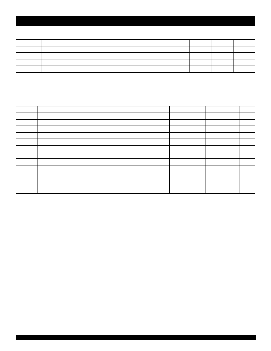
AC TIMING DIAGRAM
NOTES:
1. AC Timing Diagram applies to Q output connected to FEEDBACK and
PE
= GND. For
PE
= V
DD
, the negative edge of FEEDBACK aligns with the
negative edge of SYNC input, and the negative edges of the multiplied and divided outputs align with the negative edge of SYNC.
2. All parameters are measured at 1.5V.
S YN C
FEE DB A CK
Q
Q
0
-Q
4
Q /2
2xQ
Q
5
t
SK F
t
SKA LL
t
S KR
t
J
t
PD
8
INDUSTRIAL TEMPERATURE RANGE
QS5919T
LOW SKEW TTL PLL CLOCK DRIVER WITH INTEGRATED LOOP FILTER
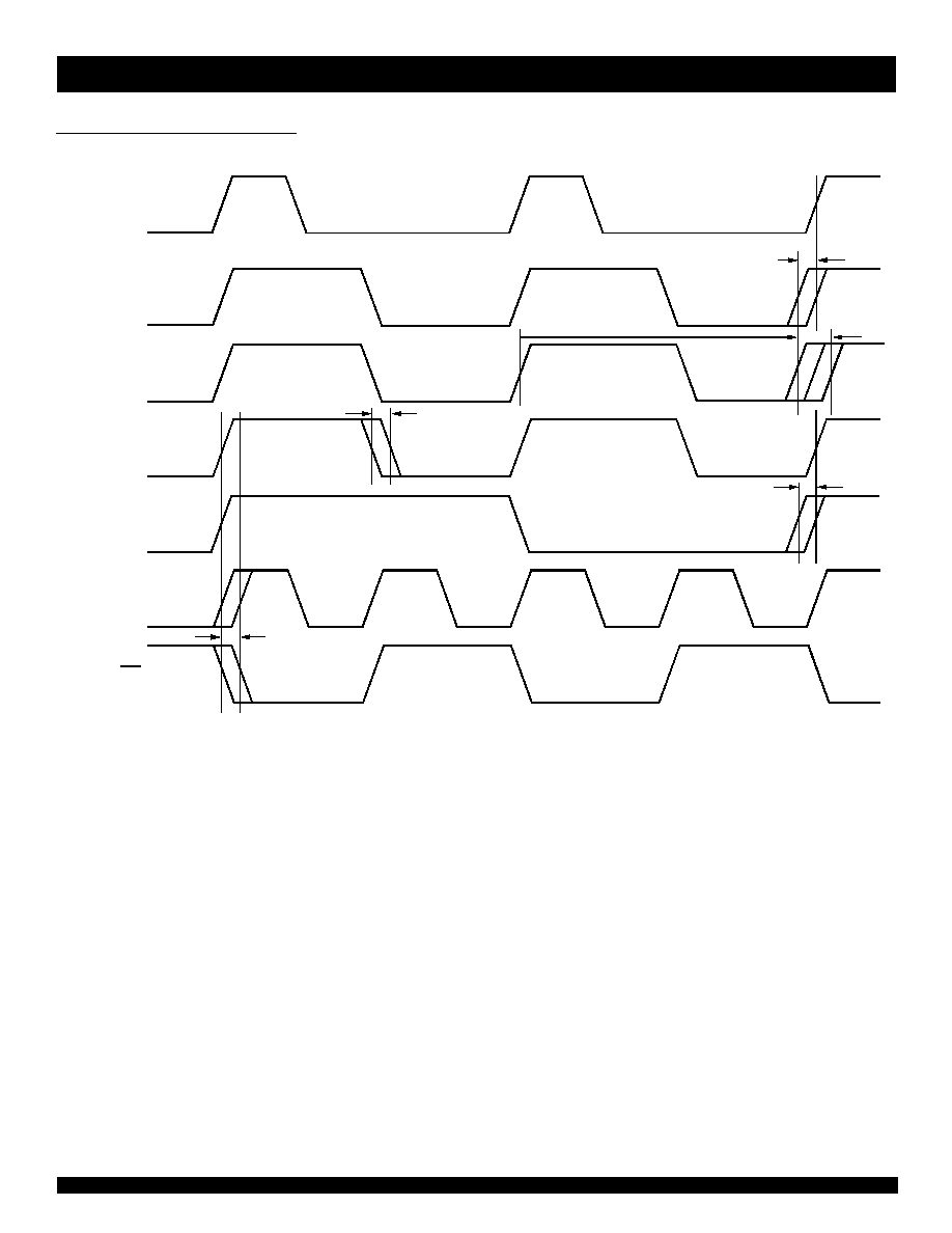
PLL OPERATION
The Phase Locked Loop (PLL) circuit included in the QS5919T
provides for replication of incoming SYNC clock signals. Any manipulation
of that signal, such as frequency multiplying or inversion is performed by
digital logic following the PLL (see the block diagram). The key advantage
SIMPLIFIED DIAGRAM OF QS5919T FEEDBACK
The phase difference between the output and the input frequencies
feeds the VCO which drives the outputs. Whichever output is fed back, it
will stabilize at the same frequency as the input. Hence, this is a true
negative feedback closed loop system. In most applications, the output will
optimally have zero phase shift with respect to the input. In fact, the internal
loop filter on the QS5919T typically provides within 150ps of phase shift
between input and output.
of the PLL circuit is to provide an effective zero propagation delay between
the output and input signals. In fact, adding delay circuits in the feedback
path, `propagation delay' can even be negative! A simplified schematic
of the QS5919T PLL circuit is shown below.
If the user wishes to vary the phase difference (typically to compensate
for backplane delays), this is most easily accomplished by adding delay
circuits to the feedback path. The respective output used for feedback will
be advanced by the amount of delay in the feedback path. All other outputs
will retain their proper relationships to that output.
Q
Q /
2
Q
VCO
/2
/2
PHASE
DETECTO R
INPU T
2xQ
9
INDUSTRIAL TEMPERATURE RANGE
QS5919T
LOW SKEW TTL PLL CLOCK DRIVER WITH INTEGRATED LOOP FILTER
CORPORATE HEADQUARTERS
for SALES:
2975 Stender Way
800-345-7015 or 408-727-6116
Santa Clara, CA 95054
fax: 408-492-8674
www.idt.com*
*To search for sales office near you, please click the sales button found on our home page or dial the 800# above and press 2.
The IDT logo is a registered trademark of Integrated Device Technology, Inc.
Turboclock is a registered trademark of Integrated Device Technology, Inc.
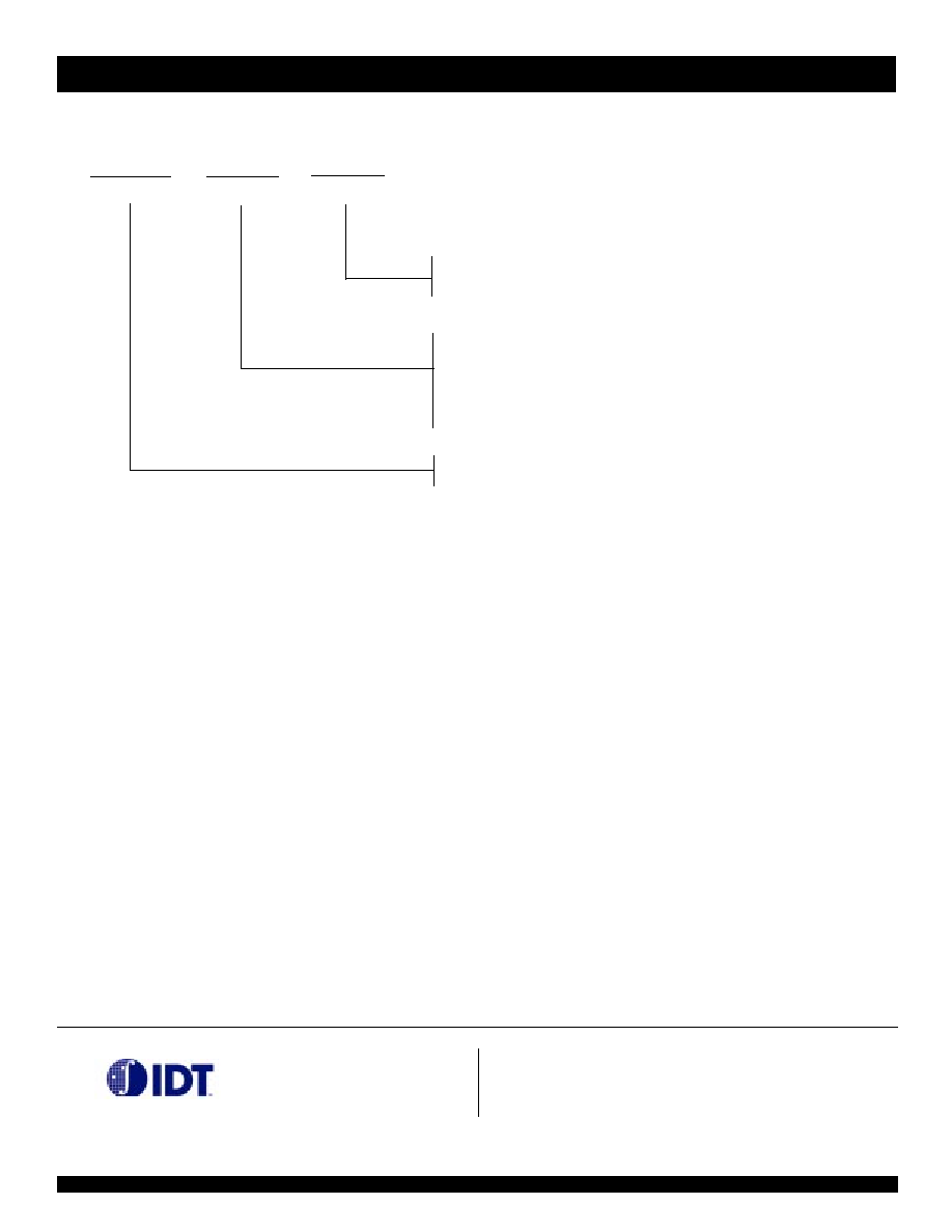
ORDERING INFORMATION
5919T
Low Skew TTL PLL Clock Driver with Integrated Loop Filter
QS
XX
Speed
XXXX
Device Type
X
Package
55
70
100
133
160
55M Hz Max. Frequency
70M Hz Max. Frequency
100MHz M ax. Frequency
133MHz M ax. Frequency
160MHz M ax. Frequency
Q
J
Quarter Size Outline Package (SO28-9)
Plastic Leaded Chip Carrier (J28-1)