
1
INDUSTRIAL TEMPERATURE RANGE
QS5LV919
3.3V LOW SKEW CMOS PLL CLOCK DRIVER WITH INTEGRATED LOOP FILTER
R
D
Q
Q
0
R
D
Q
Q
1
R
D
Q
Q
2
R
D
Q
Q
3
R
D
Q
Q
4
R
D
Q
Q
5
R
D
Q
Q /
2
Q
O E/RST
0
1
1
0
/2
VCO
LOO P
FILTER
PH A SE
DETECTO R
1
0
FREQ _SEL
REF_SEL
LO CK
FEEDBACK
SYNC
0
SYNC
1
PLL_EN
2xQ
PE
JULY 2001
2001 Integrated Device Technology, Inc.
DSC-5820/3
c
QS5LV919
INDUSTRIAL TEMPERATURE RANGE
3.3V LOW SKEW CMOS PLL
CLOCK DRIVER WITH
INTEGRATED LOOP FILTER
FUNCTIONAL BLOCK DIAGRAM
DESCRIPTION:
The QS5LV919 Clock Driver uses an internal phase locked loop
(PLL) to lock low skew outputs to one of two reference clock inputs.
Eight outputs are available: 2xQ, Q
0
-Q
4
, Q
5
, Q/2. Careful layout and
design ensure < 300 ps skew between the Q
0
-Q
4
, and Q/2 outputs.
The QS5LV919 includes an internal RC filter which provides excellent
jitter characteristics and eliminates the need for external components.
Various combinations of feedback and a divide-by-2 in the VCO path
allow applications to be customized for linear VCO operation over a
wide range of input SYNC frequencies. The PLL can also be disabled
by the PLL_EN signal to allow low frequency or DC testing. The LOCK
output asserts to indicate when phase lock has been achieved. The
QS5LV919 is designed for use in high-performance workstations, multi-
board computers, networking hardware, and mainframe systems. Sev-
eral can be used in parallel or scattered throughout a system for guar-
anteed low skew, system-wide clock distribution networks.
For more information on PLL clock driver products, see Application
Note AN-227.
FEATURES:
∑ 3.3V operation
∑ JEDEC compatible LVTTL level outputs
∑ Clock inputs are 5V tolerant
∑ < 300ps output skew, Q
0
≠Q
4
∑ 2xQ output, Q outputs, Q output, Q/2 output
∑ Outputs 3-state and reset while OE/RST low
∑ PLL disable feature for low frequency testing
∑ Internal loop filter RC network
∑ Functional equivalent to MC88LV915, IDT74FCT388915
∑ Positive or negative edge synchronization (PE)
∑ Balanced drive outputs ±24mA
∑ 160MHz maximum frequency (2xQ output)
∑ Available in QSOP and PLCC packages
The IDT logo is a registered trademark of Integrated Device Technology, Inc.

2
INDUSTRIAL TEMPERATURE RANGE
QS5LV919
3.3V LOW SKEW CMOS PLL CLOCK DRIVER WITH INTEGRATED LOOP FILTER
PIN CONFIGURATION
20
19
18
15
16
23
22
24
21
17
V
DD
GND
PLL_EN
GND
Q/2
Q
3
LOCK
V
DD
2xQ
Q
1
25
28
27
26
V
DD
Q
2
GND
Q
4
2
3
1
9
10
AV
DD
PE
OE/RST
SYNC
0
FEEDBACK
AGND
5
6
7
4
8
Q
5
11
12
FREQ_SEL
SYNC
1
GND
V
DD
REF_SEL
13
14
Q
0
GND
QSOP
TOP VIEW
PLCC
TOP VIEW
O
E
/
R
S
T
V
D
D
Q
5
G
N
D
Q
4
V
D
D
2
x
Q
Q/2
GND
Q
3
V
DD
Q
2
GND
LOCK
P
L
L
_
E
N
G
N
D
Q
1
V
D
D
Q
0
G
N
D
F
R
E
Q
_
S
E
L
FEEDBACK
REF_SEL
SYNC
0
AV
DD
PE
AGND
SYNC
1
28
4
3
2
1
27
26
25
24
23
22
21
20
19
5
6
7
8
9
10
11
12
13
14
15
16
17
18
ABSOLUTE MAXIMUM RATINGS
(1)
Symbol
Rating
Max.
Unit
V
DD
, AV
DD
Supply Voltage to Ground
≠0.5 to +7
V
DC Input Voltage V
IN
≠0.5 to +5.5
V
Maximum Power
QSOP
655
mW
Dissipation (T
A
= 85∞C) PLCC
770
mW
T
STG
Storage Temperature Range
≠65 to +150
∞C
NOTE:
1. Stresses greater than those listed under ABSOLUTE MAXIMUM RATINGS may
cause permanent damage to the device. This is a stress rating only and functional
operation of the device at these or any other conditions above those indicated in the
operational sections of this specification is not implied. Exposure to absolute maximum
rating conditions for extended periods may affect reliability.
CAPACITANCE
(T
A
= 25
∞
C, f = 1MHz, V
IN
= 0V)
QSOP
PLCC
Parameter
Typ.
Max.
Typ.
Max.
Unit
C
IN
3
4
4
6
pF
3
INDUSTRIAL TEMPERATURE RANGE
QS5LV919
3.3V LOW SKEW CMOS PLL CLOCK DRIVER WITH INTEGRATED LOOP FILTER
PIN DESCRIPTION
Pin Name
I/O
Description
SYNC
0
I
Reference clock input
SYNC
1
I
Reference clock input
REF_SEL
I
Reference clock select. When 1, selects SYNC
1
. When 0, selects SYNC
0
.
FREQ_SEL
I
VCO frequency select. For choosing optimal VCO operating frequency depending on input frequency.
FEEDBACK
I
PLL feedback input which is connected to a user selected output pin. External feedback provides flexibility for different
output frequency relationships. See the Frequency Selection Table for more information.
Q
0
-Q
4
O
Clock outputs
Q
5
O
Clock output. Matched in frequency, but inverted with respect to Q.
2xQ
O
Clock output. Matched in phase, but frequency is double the Q frequency.
Q/2
O
Clock output. Matched in phase, but frequency is half the Q frequency.
LOCK
O
PLL lock indication signal. 1 indicates positive lock. 0 indicates that the PLL is not locked and outputs may not be
synchronized to the inputs.
OE/RST
I
Output enable/asynchronous reset. Resets all output registers. When 0, all outputs are held in a tri-stated condition. When
1, outputs are enabled.
PLL_EN
I
PLL enable. Enables and disables the PLL. Useful for testing purposes.
PE
I
When PE is LOW, outputs are synchronized with the positive edge of SYNC. When HIGH, outputs are synchronized with
the negative edge of SYNC.
V
DD
--
Power supply for output buffers.
AV
DD
--
Power supply for phase lock loop and other internal circuitries.
GND
--
Ground supply for output buffers.
AGND
--
Ground supply for phase lock loop and other internal circuitries.
OUTPUT FREQUENCY SPECIFICATIONS
Industrial: T
A
= ≠40∞C to +85∞C, AV
DD
/ V
DD
= 3.3V ± 0.3V
Symbol
Description
≠ 55
≠ 70
≠ 100
≠ 133
≠ 160
Units
F
MAX_2XQ
Max Frequency, 2xQ
55
70
100
133
160
MHz
F
MAX_Q
Max Frequency, Q
0
- Q
4
, Q
5
27.5
35
50
66.5
80
MHz
F
MAX_Q/2
Max Frequency, Q/2
13.75
17.5
25
33.25
40
MHz
F
MIN_2XQ
Min Frequency, 2xQ
20
20
20
20
20
MHz
F
MIN_Q
Min Frequency, Q
0
- Q
4
, Q
5
10
10
10
10
10
MHz
F
MIN_Q/2
Min Frequency, Q/2
5
5
5
5
5
MHz
4
INDUSTRIAL TEMPERATURE RANGE
QS5LV919
3.3V LOW SKEW CMOS PLL CLOCK DRIVER WITH INTEGRATED LOOP FILTER
NOTES:
1. Operation in the specified SYNC frequency range guarantees that the VCO will operate in its optimal range of 20MHz to F
MAX_2
X
Q
. Operation with Sync inputs outside
specified frequency ranges may result in out-of-lock outputs. FREQ_SEL only affects VCO frequency and does not affect output frequencies.
2. The lock output pin (LOCK) may not indicate reliably for VCO frequencies below 30MHz.
3. The 2xQ is limited to a maximum frequency (F
MAX_2XQ
) of 100MHz only when used as a feedback.
FREQUENCY SELECTION TABLE
SYNC (MHz)
Output Used for
(allowable range)
(1)
Output Frequency Relationships
(2)
FREQ_SEL
Feedback
Min.
Max
Q/
2
Q
5
Q
0
- Q
4
2XQ
HIGH
Q/2
F
MIN_Q/2
F
MAX _Q/2
SYNC
≠ SYNC X 2
SYNC X 2
SYNC X 4
HIGH
Q
0
-Q
4
F
MIN_Q
F
MAX _Q
SYNC / 2
≠ SYNC
SYNC
SYNC X 2
HIGH
Q
5
F
MIN_Q
F
MAX _Q
≠ SYNC / 2
SYNC
≠ SYNC
≠ SYNC X 2
HIGH
2xQ
(3)
F
MIN_2XQ
100
SYNC / 4
≠ SYNC / 2
SYNC / 2
SYNC
LOW
Q/2
F
MIN_Q/2
/2
F
MAX _Q/2
/2
SYNC
≠ SYNC X 2
SYNC X 2
SYNC X 4
LOW
Q
0
-Q
4
F
MIN_Q
/2
F
MAX _Q
/2
SYNC / 2
≠ SYNC
SYNC
SYNC X 2
LOW
Q
5
F
MIN_Q
/2
F
MAX _Q
/2
≠ SYNC / 2
SYNC
≠ SYNC
≠ SYNC X 2
LOW
2xQ
F
MIN_2XQ
/2
F
MAX _2XQ
/2
SYNC / 4
≠ SYNC / 2
SYNC / 2
SYNC
Symbol
Parameter
Conditions
Min.
Typ.
Max.
Unit
V
IH
Input HIGH Voltage
Guaranteed Logic HIGH Level
2
--
--
V
V
IL
Input LOW Voltage
Guaranteed Logic LOW Level
--
--
0.8
V
V
OH
Output HIGH Voltage
I
OH
=
-
24mA
V
DD
≠ 0.6
--
--
V
I
OH
=
-
100
µA
V
DD
≠ 0.2
--
--
V
OL
Output LOW Voltage
V
DD
= Min., I
OL
= 24mA
--
--
0.45
V
V
DD
= Min., I
OL
= 100
µA
--
--
0.2
V
H
Input Hysteresis
--
--
100
--
mV
I
OZ
Output Leakage Current
V
OUT
= V
DD
or GND, V
DD
= Max.
--
--
± 5
µA
I
IN
Input Leakage Current
AV
DD
= Max., V
IN
= AV
DD
or GND
--
--
± 5
µA
I
PD
Input Pull-Down Current (PE)
AV
DD
= Max., V
IN
= AV
DD
--
--
± 100
µA
POWER SUPPLY CHARACTERISTICS
Symbol
Parameter
Test Conditions
Typ.
Max.
Unit
I
DDQ
Quiescent Power Supply Current
V
DD
= Max., OE/RST = LOW,
1
mA
SYNC = LOW, All outputs unloaded
I
DD
Power Supply Current per Input HIGH
V
DD
= Max., V
IN
= 3V
1
30
µA
I
DDD
Dynamic Power Supply Current
(1)
V
DD
= Max., C
L
= 0pF
0.2
0.4
mA/MHz
NOTE:
1. Relative to the frequency of Q outputs.
DC ELECTRICAL CHARACTERISTICS OVER OPERATING RANGE
Following Conditions Apply Unless Otherwise Specified
Industrial: T
A
= -40∞C to +85∞C, AV
DD
/V
DD
= 3.3V ± 0.3V
5
INDUSTRIAL TEMPERATURE RANGE
QS5LV919
3.3V LOW SKEW CMOS PLL CLOCK DRIVER WITH INTEGRATED LOOP FILTER
NOTES:
1. See Test Loads and Waveforms for test load and termination.
2. Skew specifications apply under identical environments (loading, temperature, V
DD
, device speed grade).
3. Measured in open loop mode PLL_EN = 0.
4. Jitter is characterized with Q output at 20MHz. See Frequency Selection Table for information on proper FREQ_SEL level for specified input frequencies.
5. Skew measured at selected synchronization edge.
6. t
PD
measured at device inputs at 0.5V
DD
, Q output at 80MHz.
INPUT TIMING REQUIREMENTS
Symbol
Description
(1)
Min.
Max.
Unit
t
R
, t
F
Maximum input rise and fall times, 0.8V to 2V
--
3
ns
F
I
Input Clock Frequency, SYNC
0
, SYNC
1
(1)
2.5
100
MHz
t
PWC
Input clock pulse, HIGH or LOW
(2)
2
--
ns
D
H
Input duty cycle, SYNC
0
, SYNC
1
(2)
25
75
%
NOTES:
1. See Output Frequency and Frequency Selection tables for more detail on allowable SYNC input frequencies for different speed grades with different FEEDBACK and
FREQ_SEL combinations.
2. Where pulse witdh implied by D
H
is less than t
WPC
limit, t
WPC
limit applies
SWITCHING CHARACTERISTICS OVER OPERATING RANGE
Symbol
Parameter
(1)
Min.
Max.
Unit
t
SKR
Output Skew Between Rising Edges, Q
0
-Q
4
(and Q/
2
if PE = LOW)
(2)
--
300
ps
t
SKF
Output Skew Between Falling Edges, Q
0
-Q
4
(and Q/
2
if PE = HIGH)
(2)
--
300
ps
t
SKALL
Output Skew, All Outputs
(2, 5)
--
500
ps
t
PW
Pulse Width, 2xQ output, >40MHz
T
CY
/2
-
0.4
T
CY
/2 + 0.4
ns
t
PW
Pulse Width, Q
0
-Q
4
, Q
5,
Q/2 outputs, 80MHz
T
CY
/2
-
0.4
T
CY
/2 + 0.4
ns
t
J
Cycle-to-Cycle Jitter
(4)
-
0.15
0.15
ns
t
PD
SYNC Input to Feedback Delay
(6)
-
500
0
ps
t
LOCK
SYNC to Phase Lock
--
10
ms
t
PZH
Output Enable Time, OE/RST LOW to HIGH
(3)
0
14
ns
t
PZL
t
PHZ
Output Disable Time, OE/RST HIGH to LOW
(3)
0
14
ns
t
PLZ
t
R,
t
F
Output Rise/Fall Times, 0.8V
2V
0.3
2
ns
6
INDUSTRIAL TEMPERATURE RANGE
QS5LV919
3.3V LOW SKEW CMOS PLL CLOCK DRIVER WITH INTEGRATED LOOP FILTER
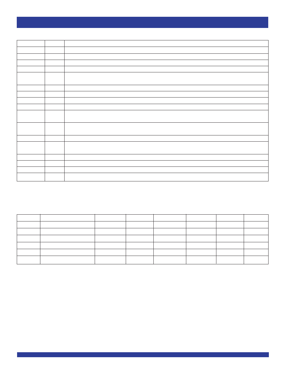
ANALO G V
C C
ANALO G G ND
DIG ITAL
G ND
DIG ITAL
V
C C
BO ARD G ND
BO AR D V
C C
0.1
µ
F
High
Freq.
Bypass
10
µ
F
Low
Freq.
B ypass
A separate A nalog power supply is not necessary
and should not be used. Following these pre-
scribed guidelines is all that is necessary to use
the Q S5LV919 in a norm al digital environment.
0.1
µ
F
Bypass
Figure 1. Recommended Analog Isolation Scheme for the QS5LV919
NOTES:
1. Figure 1 shows an analog isolation scheme which will be effective in most applications. The following guidelines should be followed to ensure stable and jitter-free operation:
a. All analog isolation components should be tied as close to the package as possible. Stray current passing through the parasitics of long traces can cause undesirable voltage
transients.
b. The 10µF low frequency bypass capacitor and the 0.1µF high frequency bypass capacitor form a wide bandwidth filter that will minimize the QS5LV919's sensitivity to voltage
transients from the system digital V
CC
supply and ground planes.
If good bypass techniques are used on a board design near components which may cause digital V
CC
and ground noise, V
CC
step deviations should not occur at the QS5LV919's
digital V
CC
supply. The purpose of the bypass filtering scheme shown in figure 1 is to give the QS5LV919 additional protection from the power supply and ground plane
transients that can occur in a high frequency, high speed digital system.
2. The bypass capacitors can be ceramic chip capacitors. There should be a 0.1µF bypass capacitor between each of the other (digital) four V
CC
pins and the board ground plane.
This will reduce output switching noise caused by the QS5LV919 outputs, in addition to reducing potential for noise in the "analog" section of the chip. These bypass capacitors
should also be tied as close to the QS5LV919 package as possible.
7
INDUSTRIAL TEMPERATURE RANGE
QS5LV919
3.3V LOW SKEW CMOS PLL CLOCK DRIVER WITH INTEGRATED LOOP FILTER
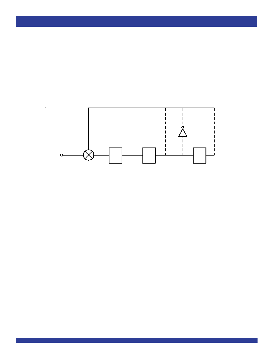
PLL OPERATION
The Phase Locked Loop (PLL) circuit included in the QS5LV919 provides
for replication of incoming SYNC clock signals. Any manipulation of that
signal, such as frequency multiplying or inversion is performed by digital
logic following the PLL (see the block diagram). The key advantage of the
SIMPLIFIED DIAGRAM OF QS5LV919 FEEDBACK
The phase difference between the output and the input frequencies feeds
the VCO which drives the outputs. Whichever output is fed back, it will
stabilize at the same frequency as the input. Hence, this is a true negative
feedback closed loop system. In most applications, the output will optimally
have zero phase shift with respect to the input. In fact, the internal loop filter
on the QS5LV919 typically provides within 150ps of phase shift between
input and output.
PLL circuit is to provide an effective zero propagation delay between the
output and input signals. In fact, adding delay circuits in the feedback path,
`propagation delay' can even be negative! A simplified schematic of the
QS5LV919 PLL circuit is shown below.
If the user wishes to vary the phase difference (typically to compensate
for backplane delays), this is most easily accomplished by adding delay
circuits to the feedback path. The respective output used for feedback will
be advanced by the amount of delay in the feedback path. All other outputs
will retain their proper relationships to that output.
Q
Q /2
Q
VCO
/2
/2
PHASE
DETECTO R
INPU T
2xQ
8
INDUSTRIAL TEMPERATURE RANGE
QS5LV919
3.3V LOW SKEW CMOS PLL CLOCK DRIVER WITH INTEGRATED LOOP FILTER
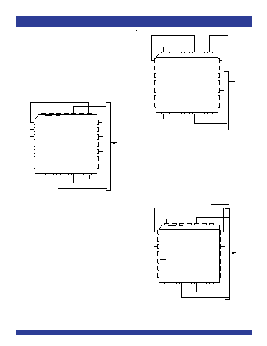
The frequency relationship shown here is applicable to all Q outputs (Q0, Q1,
Q2, Q3 and Q4).
1:2 INPUT TO "Q" OUTPUT FREQUENCY RELATIONSHIP
In this application, the Q/2 output is connected to the FEEDBACK input. The
internal PLL will line up the positive edges of Q/2 and SYNC, thus the Q/2
frequency will equal the SYNC frequency. The Q outputs (Q0-Q4, Q5) will
always run at 2X the Q/2 frequency, and the 2Q output will run at 4X the Q/2
frequency.
Allowable Input Frequency Range:
20MHz to (f2Q MAX Spec)/2 (for FREQ_SEL HIGH)
10MHz to (f2Q MAX Spec)/4 (for FREQ_SEL LOW)
Figure 2c. Wiring Diagram and Frequency Relationships with
Q2 Output Feedback
Figure 2b. Wiring Diagram and Frequency Relationships with
Q4 Output Feedback
Allowable Input Frequency Range:
10MHz to ( f2Q MAX Spec)/4 (for FREQ_SEL HIGH)
5MHz to (f2Q MAX Spec)/8 (for FREQ_SEL LOW)
Q/2
Q3
Q2
PLL_EN
Q1
Q0
FQ_SEL
FEEDBACK
REF_SEL
SYNC(0)
V
CC
(AN)
GND(AN)
Q 4
Q5
2Q
LOW
50 MHz signal
12.5 MHz feedback signal
HIGH
HIGH
HIGH
25 MHz
"Q"
Clock
Outputs
12.5 MHz
input
PE
QS5LV919
RST
OE/
Q/2
Q3
Q2
PLL_EN
Q1
Q0
FQ_SEL
FEEDBACK
REF_SEL
SYNC(0)
V
C C
(AN)
GND(AN)
Q4
Q5
2Q
LOW
50 M Hz signal
25 M Hz feedback signal
HIGH
HIGH
HIGH
25 MHz
"Q"
Clock
Outputs
25 M Hz
input
12.5 MHz
signal
PE
QS5LV919
RST
OE/
Allowable Input Frequency Range:
40MHz to (f2Q MAX Spec) (for FREQ_SEL HIGH)
20MHz to (f2Q MAX Spec)/2 (for FREQ_SEL LOW)
2:1 INPUT TO "Q" OUTPUT FREQUENCY RELATIONSHIP
In this application, the 2Q output is connected to the FEEDBACK input. The
internal PLL will line up the positive edges of 2Q and SYNC, thus the 2Q
frequency will equal the SYNC frequency. The Q/2 output will always run at
1/4 the 2Q frequency, and the Q output will run at 1/2 the 2Q frequency.
Note that with 2Q as feedback, the maximum input frequency is 100MHz for FS
= HIGH
Figure 2a. Wiring Diagram and Frequency Relationships with 2Q
Output Feedback
Q /2
Q 3
Q2
PLL_EN
Q 1
Q 0
FQ_SEL
FEED BACK
REF_SEL
SYNC(0)
V
C C
(AN)
GND(AN)
Q 4
Q5
2Q
LOW
50 MHz feedback signal
HIGH
HIG H
HIGH
25 MHz
"Q"
Clock
O utputs
50 MHz
input
12.5 MHz
input
PE
Q S5LV919
RST
O E/
1:1 INPUT TO "Q" OUTPUT FREQUENCY RELATIONSHIP
In this application, the Q4 output is connected to the FEEDBACK input. The
internal PLL will line up the positive edges of Q4 and SYNC, thus the Q4
frequency (and the rest of the "Q" outputs) will equal the SYNC frequency. The
Q/2 output will always run at 1/2 the Q frequency, and the 2Q output will run
at 2X the Q frequency.
9
INDUSTRIAL TEMPERATURE RANGE
QS5LV919
3.3V LOW SKEW CMOS PLL CLOCK DRIVER WITH INTEGRATED LOOP FILTER
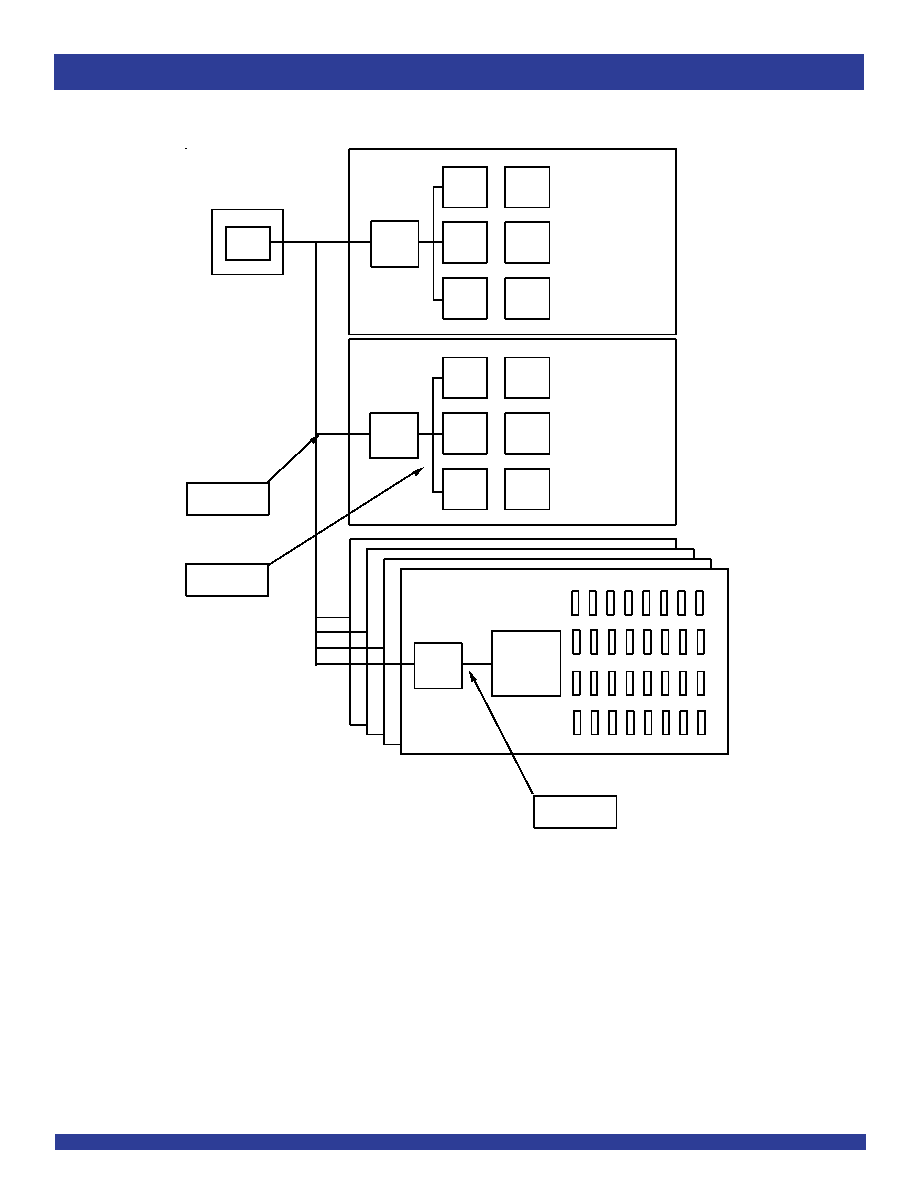
CM MU
CM M U
CPU
CM M U
CM MU
CM M U
CM MU
CM M U
CPU
CM M U
CM MU
CM M U
PLL
2f
PLL
2f
CPU
CARD
CPU
CARD
CLOCK
@ f
SYS TEM
CLO CK
SO URCE
QS5LV919
QS5LV919
DISTRIBUTE
CLO CK @ f
CLOCK @ 2f
at point of use
M EM O RY
CO NTROL
PLL
2f
ME MO RY
CAR DS
CLO CK @ 2f
at point of use
QS5LV919
Figure 3. Multiprocessing Application Using the QS5LV919 for Frequency Multiplication and Low Board-to-Board skew
QS5LV919 System Level Testing Functionality
When the PLL_EN pin is LOW, the PLL is bypassed and the QS5LV919 is
in low frequency "test mode". In test mode (with FREQ_SEL HIGH), the 2Q
output is inverted from the selected SYNC input, and the Q outputs are divide-
by-2 (negative edge triggered) of the SYNC input, and the Q/2 output is divide-
by-4 (negative edge triggered). With FREQ_SEL LOW the 2Q output is divide-
by-2 of the SYNC, the Q outputs divide-by-4, and the Q/2 output divide-by-8.
These relationships can be seen in the block diagram. A recommended test
configuration would be to use SYNC0 or SYNC1 as the test clock input, and tie
PLL_EN and REF_SEL together and connect them to the test select logic.
This functionality is needed since most board-level testers run at 1 MHz or
below, and the QS5LV919 cannot lock onto that low of an input frequency. In
the test mode described above, any test frequency test can be used.
10
INDUSTRIAL TEMPERATURE RANGE
QS5LV919
3.3V LOW SKEW CMOS PLL CLOCK DRIVER WITH INTEGRATED LOOP FILTER
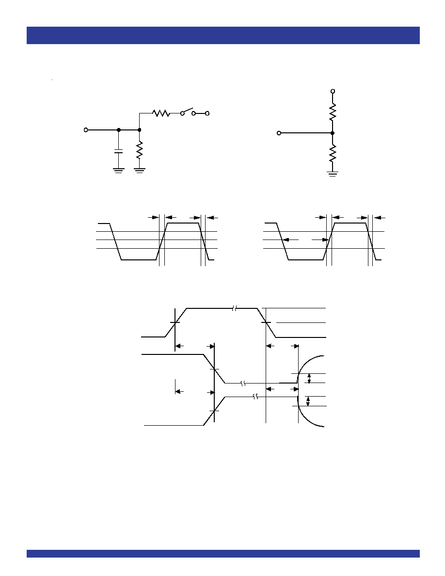
1.0ns
1.0ns
2.0V
0.8V
3.0V
0V
V
th
= 0.5V
DD
t
P W
t
R
t
F
CONTROL
INPU T
EN ABLE
DISABLE
3V
0V
3.0V
V
O L
0V
t
P Z L
OUTPUT
NOR MALLY
LOW
OUTPUT
NOR MALLY
HIGH
SWITCH
OPEN
SWITCH
CLO SED
0.3V
0.3V
t
PZ H
t
PLZ
t
P HZ
V
O H
300
30pF
7.0V
OUTPUT
V
D D
OUTPUT
300
100
100
2.0V
0.8V
3.0V
0V
0.5V
D D
0.5V
D D
0.5V
DD
0.5V
D D
AC TEST LOADS AND WAVEFORMS
TEST CIRCUIT 1
LVTTL INPUT TEST WAVEFORM
LVTTL OUTPUT WAVEFORM
TEST CIRCUIT 2
ENABLE AND DISABLE TIMES
TEST CIRCUIT 1 is used for output enable/disable parameters.
TEST CIRCUIT 2 is used for all other timing parameters.

11
INDUSTRIAL TEMPERATURE RANGE
QS5LV919
3.3V LOW SKEW CMOS PLL CLOCK DRIVER WITH INTEGRATED LOOP FILTER
t
J
SY NC
FEE DB ACK
Q
Q
0
-Q
4
Q /2
2xQ
Q
5
t
S K F
t
S K A LL
t
S K R
t
P D
AC TIMING DIAGRAM
NOTES:
1. AC Timing Diagram applies to Q output connected to FEEDBACK and PE = GND. For PE = V
DD
, the negative edge of FEEDBACK aligns with the negative edge of SYNC
input, and the negative edges of the multiplied and divided outputs align with the negative edge of SYNC.
2. All parameters are measured at 0.5V
DD.
12
INDUSTRIAL TEMPERATURE RANGE
QS5LV919
3.3V LOW SKEW CMOS PLL CLOCK DRIVER WITH INTEGRATED LOOP FILTER
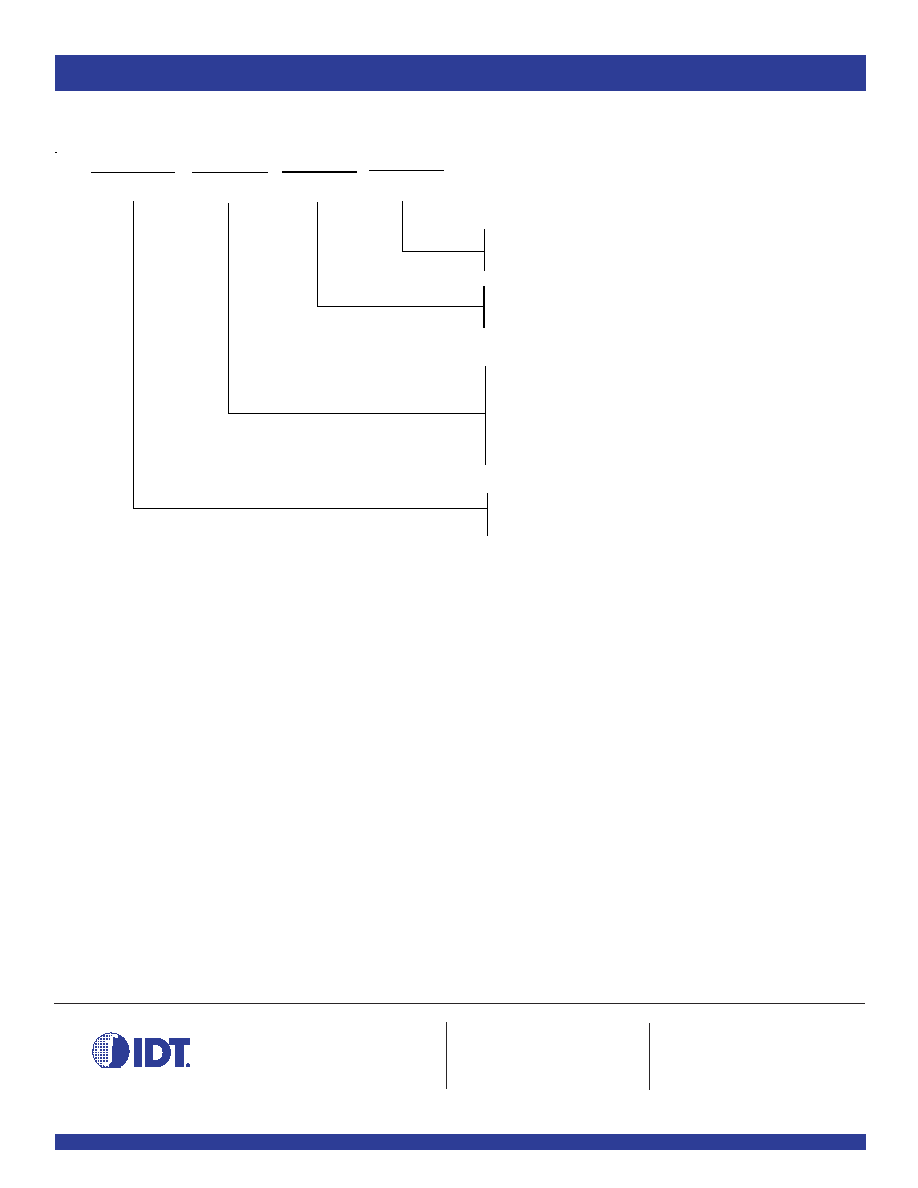
ORDERING INFORMATION
QS
XX
Speed
5LV919 Low Skew CMOS PLL Clock Driver
with Integrated Loop Filter
XXXX
Device Type
X
Package
55
70
100
133
160
55MHz Max. Frequency
70MHz Max. Frequency
100MHz Max. Frequency
133MHz Max. Frequency
160MHz Max. Frequency
Q
J
Quarter Size Outline Package
Plastic Leaded Chip Carrier
X
Process
Blank
Industrial (-40∞C to +85∞C)
CORPORATE HEADQUARTERS
for SALES:
for Tech Support:
2975 Stender Way
800-345-7015 or 408-727-6116
logichelp@idt.com
Santa Clara, CA 95054
fax: 408-492-8674
(408) 654-6459
www.idt.com