1
IDTQS74FCT2841AT/BT/CT
HIGH-SPEED CMOS BUS INTERFACE 10-BIT LATCH
INDUSTRIAL TEMPERATURE RANGE
MARCH 2002
2002 Integrated Device Technology, Inc.
DSC-5260/4
c
IDTQS74FCT2841AT/BT/CT
INDUSTRIAL TEMPERATURE RANGE
HIGH-SPEED CMOS
BUS INTERFACE
10-BIT LATCH
DESCRIPTION:
The IDTQS74FCT2841T is a 10-bit high-speed CMOS TTL-compatible
buffered latch with 3-state outputs, with a 25
resister that is useful for driving
transmission lines and reducing system noise. The 2841 eliminates the need
for external series resistors in high speed systems and can replace the 841
series to reduce noise in an existing design. All inputs have clamp diodes
for undershoot noise suppression. All outputs have ground bounce
suppression. Outputs will not load an active bus when Vcc is removed from
the device.
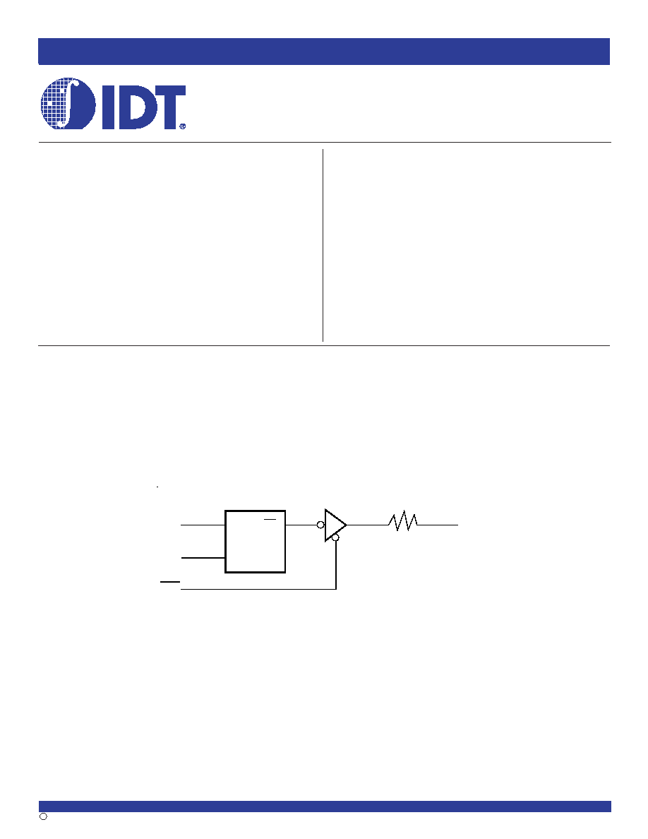
FUNCTIONAL BLOCK DIAGRAM
OE
D
LE
Q
LE
Dx
Yx
25
FEATURES:
∑ CMOS power levels: <7.5mW static
∑ Undershoot clamp diodes on all outputs
∑ True TTL input and output compatibility
∑ Ground bounce controlled outputs
∑ Reduced output swing of 0 to 3.5V
∑ Built-in 25
series resistor outputs reduce reflection and other
system noise
∑ A, B, and C speed grades with 5.5ns t
PD
for C
∑ I
OL
= 12mA
∑ Available in SOIC and QSOP packages
2
INDUSTRIAL TEMPERATURE RANGE
IDTQS74FCT2841AT/BT/CT
HIGH-SPEED CMOS BUS INTERFACE 10-BIT LATCH
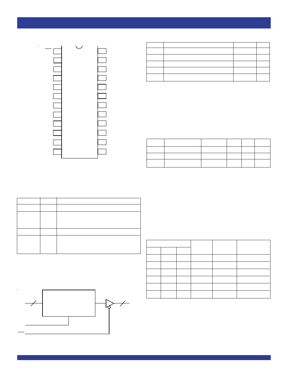
SOIC/ QSOP
TOP VIEW
2
3
1
V
CC
20
19
18
15
16
23
22
24
21
17
Y
2
Y
4
Y
3
Y
6
Y
5
Y
1
Y
7
Y
8
13
14
LE
Y
9
Y
0
D
4
D
5
D
3
D
7
D
6
D
1
D
2
D
8
9
10
5
6
7
4
8
11
12
GND
OE
D
0
D
9
PIN CONFIGURATION
Symbol
Description
Max
Unit
V
TERM
Terminal Voltage with Respect to GND
≠0.5 to +7
V
T
STG
Storage Temperature
≠65 to +150
∞C
I
OUT
DC Output Current Max Sink Current/Pin
120
mA
I
IK
Input Diode Current, V
IN
< 0
≠20
mA
I
OK
Output Diode Current, V
OUT
< 0
≠50
mA
ABSOLUTE MAXIMUM RATINGS
(1)
NOTE:
1. Stresses greater than those listed under ABSOLUTE MAXIMUM RATINGS may cause
permanent damage to the device. This is a stress rating only and functional operation
of the device at these or any other conditions above those indicated in the operational
sections of this specification is not implied. Exposure to absolute maximum rating
conditions for extended periods may affect reliability.
CAPACITANCE
(T
A
= +25∞C, F = 1.0MHz)
NOTES:
1. This parameter is measured at characterization but not tested.
2. Pins 1-11, 13.
3. Pins 15-22.
4. Pins 14, 23.
PIN DESCRIPTION
Pin Names
I/O
Description
Dx
I
Latch Data Inputs
LE
I
The latch enable input. The latches are transparent when
LE is HIGH. Input data is latched on the HIGH-to-LOW
transition.
Y x
O
3-State Latch Outputs
OE
I
The output enable control. When OE is LOW, the outputs
are enabled. When OE is HIGH, the outputs Yx are in
high-impedance (off) state.
Symbol
Parameter
(1)
Conditions
Typ.
Max.
Unit
C
IN
(2)
Input Capacitance
V
IN
= 0V
4
--
pF
C
OUT
(3)
Output Capacitance
V
OUT
= 0V
6
--
pF
C
OUT
(4)
Output Capacitance
V
OUT
= 0V
4
--
pF
FUNCTION TABLE
(1)
Inputs
Internal
Outputs
OE
LE
Dx
Value Qx
Yx
Function
H
H
L
L
Z
High-Z
H
H
H
H
Z
High-Z
H
L
X
N C
Z
Latched (High-Z)
L
H
L
L
L
Transparent
L
H
H
H
H
Transparent
L
L
X
N C
N C
Latched
NOTE:
1. H = HIGH Voltage Level
L = LOW Voltage Level
X = Don't Care
NC = No Change
Z = High-Impedance
LOGIC SYMBOL
Dx
LE
OE
D
Q
Yx
LE
10
10

3
IDTQS74FCT2841AT/BT/CT
HIGH-SPEED CMOS BUS INTERFACE 10-BIT LATCH
INDUSTRIAL TEMPERATURE RANGE
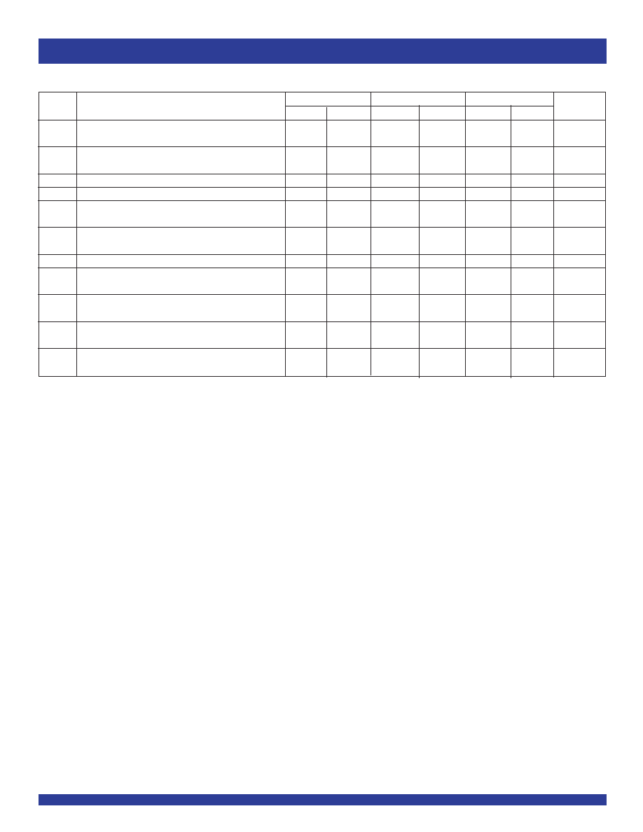
Symbol
Parameter
Test Conditions
Min.
Typ.
(1)
Max.
Unit
V
IH
Input HIGH Level
Guaranteed Logic HIGH Level
2
--
--
V
V
IL
Input LOW Level
Guaranteed Logic LOW Level
--
--
0.8
V
V
T
Input Hysteresis
V
TLH
- V
THL
for all inputs
--
0.2
--
V
I
IH
Input HIGH Current
V
CC
= Max.
0
V
IN
V
CC
--
--
±5
µA
I
IL
Input LOW Current
I
OZ
Off-State Output Current (Hi-Z)
V
CC
= Max
0
V
IN
V
CC
--
--
±5
µA
I
OR
Current Drive
V
CC
= Max., V
OUT
= 2.0V
(2)
50
--
--
mA
V
IC
Input Clamp Voltage
V
CC
= Min, I
IN
= -18mA , T
A
= 25∞C
(2)
--
≠0.7
≠1.2
V
V
OH
Output HIGH Voltage
V
CC
= Min.
I
OH
= -15mA
2.4
--
--
V
V
OL
Output LOW Voltage
V
CC
= Min.
I
OL
= 12mA
--
--
0.5
V
R
OUT
(3)
Output Resistance
V
CC
= Min.
I
OH
= 12mA
18
25
40
DC ELECTRICAL CHARACTERISTICS OVER OPERATING RANGE
Following Conditions Apply Unless Otherwise Specified:
Industrial: T
A
= ≠40∞C to +85∞C, V
CC
= 5.0V ±5%
NOTES:
1. Typical values are at V
CC
= 5.0V, T
A
= 25∞C.
2. This parameter is measured at characterization but not tested.
3. R
OUT
changed on March 8, 2002. See rear page for more information.
POWER SUPPLY CHARACTERISTICS
Following Conditions Apply Unless Otherwise Specified:
Industrial: T
A
= -40∞C to +85∞C, V
CC
= 5.0V ± 5%
Symbol
Parameter
Test Conditions
(1)
Min.
Max.
Unit
I
CC
Quiescent Power Supply Current
V
CC
= Max.
--
1.5
mA
freq = 0
0V
V
IN
0.2V or
V
CC
- 0.2V
V
IN
Vcc
I
CC
Supply Current per Input TTL Inputs HIGH
V
CC
= Max.
--
2
mA
V
IN
= 3.4V
(2)
freq = 0
I
CCD
Supply Current per Input per MHz
V
CC
= Max.
--
0.25
mA/MHz
Outputs Open and Enabled
One Bit Toggling
50% Duty Cycle
Other inputs at GND or Vcc
(3,4)
NOTES:
1. For conditions shown as Min. or Max., use the appropriate values specified under DC Electrical Characteristics.
2. Per TLL driven input (V
IN
= 3.4V).
3. For flip-flops, I
CCD
is measured by switching one of the data input pins so that the output changes every clock cycle. This is a measurement of device power consumption
only and does not include power to drive load capacitance or tester capacitance.
4. I
C
= I
QUIESCENT
+ I
INPUTS
+ I
DYNAMIC
I
C
= I
CC
+
I
CC
D
H
N
T
+ I
CCD
(f
CP
/2 + f
i
N
i
)
I
CC
= Quiescent Current
I
CC
= Power Supply Current for a TTL High Input (V
IN
= 3.4V)
D
H
= Duty Cycle for TTL Inputs High
N
T
= Number of TTL Inputs at D
H
I
CCD
= Dynamic Current Caused by an Output Transition Pair (HLH or LHL)
f
CP
= Clock Frequency for Register Devices (Zero for Non-Register Devices)
f
i
= Input Frequency
N
i
= Number of Inputs at f
i
All currents are in milliamps and all frequencies are in megahertz.
4
INDUSTRIAL TEMPERATURE RANGE
IDTQS74FCT2841AT/BT/CT
HIGH-SPEED CMOS BUS INTERFACE 10-BIT LATCH
FCT2841AT
FCT2841BT
FCT2841CT
Symbol
Parameter
(2)
Min.
Max.
Min.
Max.
Min.
Max.
Unit
t
PLH
Data to Y Delay
--
9.5
--
6.5
--
5.5
ns
t
PHL
OE = LOW
t
PLH
Data to Y Delay
(3,4)
--
20
--
13
--
13
ns
t
PHL
OE = LOW
t
SU
Data to LE Setup Time
2.5
--
2.5
--
2.5
--
ns
t
H
Data to LE Hold Time
2.5
--
2.5
--
2.5
--
ns
t
LEY
LE to Y Delay
--
12
--
8
--
8
ns
OE = LOW
t
LEY
LE to Y Delay
(3,4)
--
16
--
15.5
--
15
ns
OE = LOW
t
W
LE Pulse Width, HIGH
(3)
6
--
4
--
4
--
ns
t
PZH
Output Enable Time
--
11.5
--
8
--
6.5
ns
t
PZL
OE
to Yx
t
PZH
Output Enable Time
(3,4)
--
23
--
14
--
12
ns
t
PZL
OE
to Yx
t
PHZ
Output Disable Time
(3,5)
--
7
--
6
--
5.7
ns
t
PLZ
OE
to Yx
t
PHZ
Output Disable Time
(3)
--
8
--
7
--
6
ns
t
PLZ
OE
to Yx
SWITCHING CHARACTERISTICS OVER OPERATING RANGE
(1)
NOTES:
1. C
LOAD
= 50pF, R
LOAD
= 500
unless otherwise noted.
2. See Test Circuits and Waveforms
3. This parameter is guaranteed by design but not tested.
4. C
LOAD
= 300pF.
5. C
LOAD
= 5pF.
5
IDTQS74FCT2841AT/BT/CT
HIGH-SPEED CMOS BUS INTERFACE 10-BIT LATCH
INDUSTRIAL TEMPERATURE RANGE
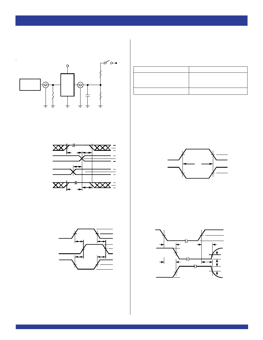
Pulse
Generator
R
T
D.U.T.
V
CC
V
IN
C
L
V
OUT
50pF
500
500
7.0V
3V
1.5V
0V
3V
1.5V
0V
3V
1.5V
0V
3V
1.5V
0V
DATA
INPUT
TIMING
INPUT
ASYNCHRONOUS CONTROL
PRESET
CLEAR
ETC.
SYNCHRONOUS CONTROL
t
SU
t
H
t
REM
t
SU
t
H
HIGH-LOW-HIGH
PULSE
LOW-HIGH-LOW
PULSE
t
W
1.5V
1.5V
SAME PHASE
INPUT TRANSITION
3V
1.5V
0V
1.5V
V
OH
t
PLH
OUTPUT
OPPOSITE PHASE
INPUT TRANSITION
3V
1.5V
0V
t
PLH
t
PHL
t
PHL
V
OL
CONTROL
INPUT
3V
1.5V
0V
3.5V
0V
OUTPUT
NORMALLY
LOW
OUTPUT
NORMALLY
HIGH
SWITCH
CLOSED
SWITCH
OPEN
V
OL
0.3V
0.3V
t
PLZ
t
PZL
t
PZH
t
PHZ
3.5V
0V
1.5V
1.5V
ENABLE
DISABLE
V
OH
PRESET
CLEAR
CLOCK ENABLE
ETC.
FCTL link
FCTL link
FCTL link
FCTL link
FCTL link
TEST CIRCUITS AND WAVEFORMS
Propagation Delay
Enable and Disable Times
Set-Up, Hold, and Release Times
Pulse Width
NOTES:
1. Diagram shown for input Control Enable-LOW and input Control Disable-HIGH.
2. Pulse Generator for All Pulses: Rate
1.0MHz; t
F
2.5ns; t
R
2.5ns.
Test
Switch
Open Drain
Disable Low
Closed
Enable Low
All Other Tests
Open
SWITCH POSITION
DEFINITIONS:
C
L
= Load capacitance: includes jig and probe capacitance.
R
T
= Termination resistance: should be equal to Z
OUT
of the Pulse Generator.
Test Circuits for All Outputs
6
INDUSTRIAL TEMPERATURE RANGE
IDTQS74FCT2841AT/BT/CT
HIGH-SPEED CMOS BUS INTERFACE 10-BIT LATCH
ORDERING INFORMATION
SO
Q
Small Outline IC (gull wing)
Quarter Size Small Outline Package
High-Speed CMOS Bus Interface 10-Bit Latch
2841AT
2841BT
2841CT
74
≠40∞C to +85∞C
IDTQS
XX
FCT
XXXX
XX
Package
Device Type
Temp. Range
CORPORATE HEADQUARTERS
for SALES:
for Tech Support:
2975 Stender Way
800-345-7015 or 408-727-6116
logichelp@idt.com
Santa Clara, CA 95054
fax: 408-492-8674
(408) 654-6459
www.idt.com
Parameter
Description
Min.
Typ.
Max.
Unit
R
OUT
V
CC
= Min, I
OL
= -15mA
20
28
40
As per PCN L0201-02, the Output Resistance (R
OUT
) specifications have changed as of March 8, 2002. The original specifications were: