Technical Data
Low Drop Regulator with Signal
IK31001
Interface Logic Circuit
DESCRIPTION
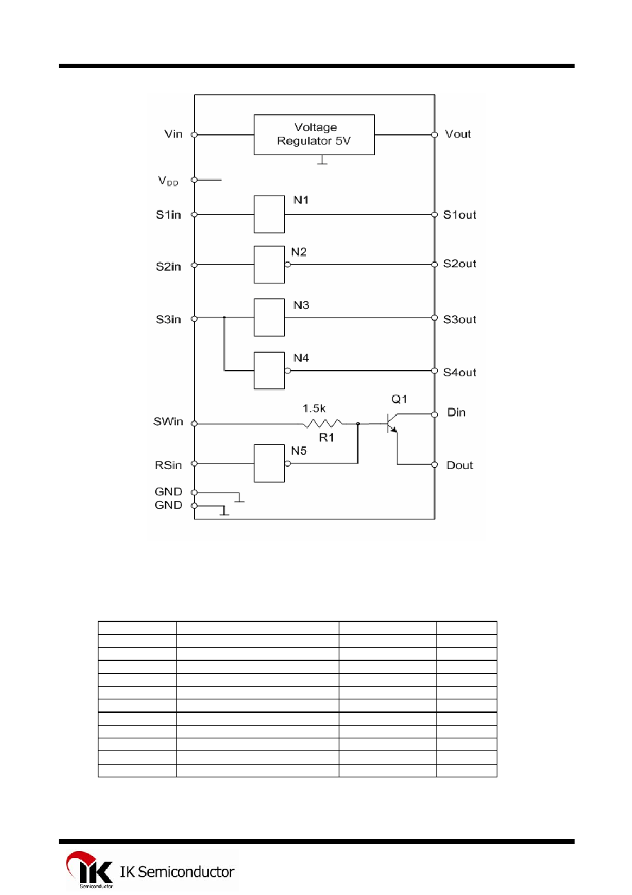
The IC is linear voltage regulator 5V with low dropout voltage typically
100mV at light loads and less then 500mV at full loads, with better then 4%
output voltage accuracy. In additional IC have logical blokes for additional
functions.
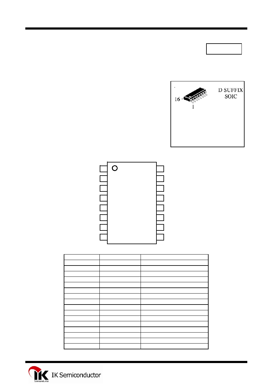
ORDERING INFORMATION
IK31001 SOIC
T
A
= -40
∞ to 85∞C for package
FEATURES
∑
Voltage
regulator 5V with 4% output voltage accuracy
∑
Low dropout voltage 0.7V Max
∑
Load current 200mA Max
∑
Low Standby Current Consumption : 500
∑
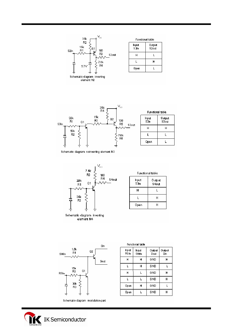
Logical blokes for internal back light control
PIN DIAGRAM
PIN NAME
FUNCTION
01 V
DD
Power supply logic blokes
02 S3out
Output
S3out
03 S1out
Output
S1out
04 S1in
Input
S1in
05 GND
Ground
06
Vout
Output regulator voltage 5V
07 Din
Input
Din
08 Dout
Output
Dout
09 Swin
Input
Swin
10 Rsin
Input
Rsin
11 GND
Ground
12
Vin
Input voltage
13 S2out
Output
S2out
14 S2in
Input
S2in
15 S4out
Output
S4out
16 S3in
Input
S3in
16
01
Vin
Vout
GND
V
DD
S1out
S2out
S4out
S3out
Din
Dout
GND
Rsin
Swin
S3in
02
S2in
S1in
15
03
14
04
13
05
12
06
11
07
10
08
09
1
IK31001
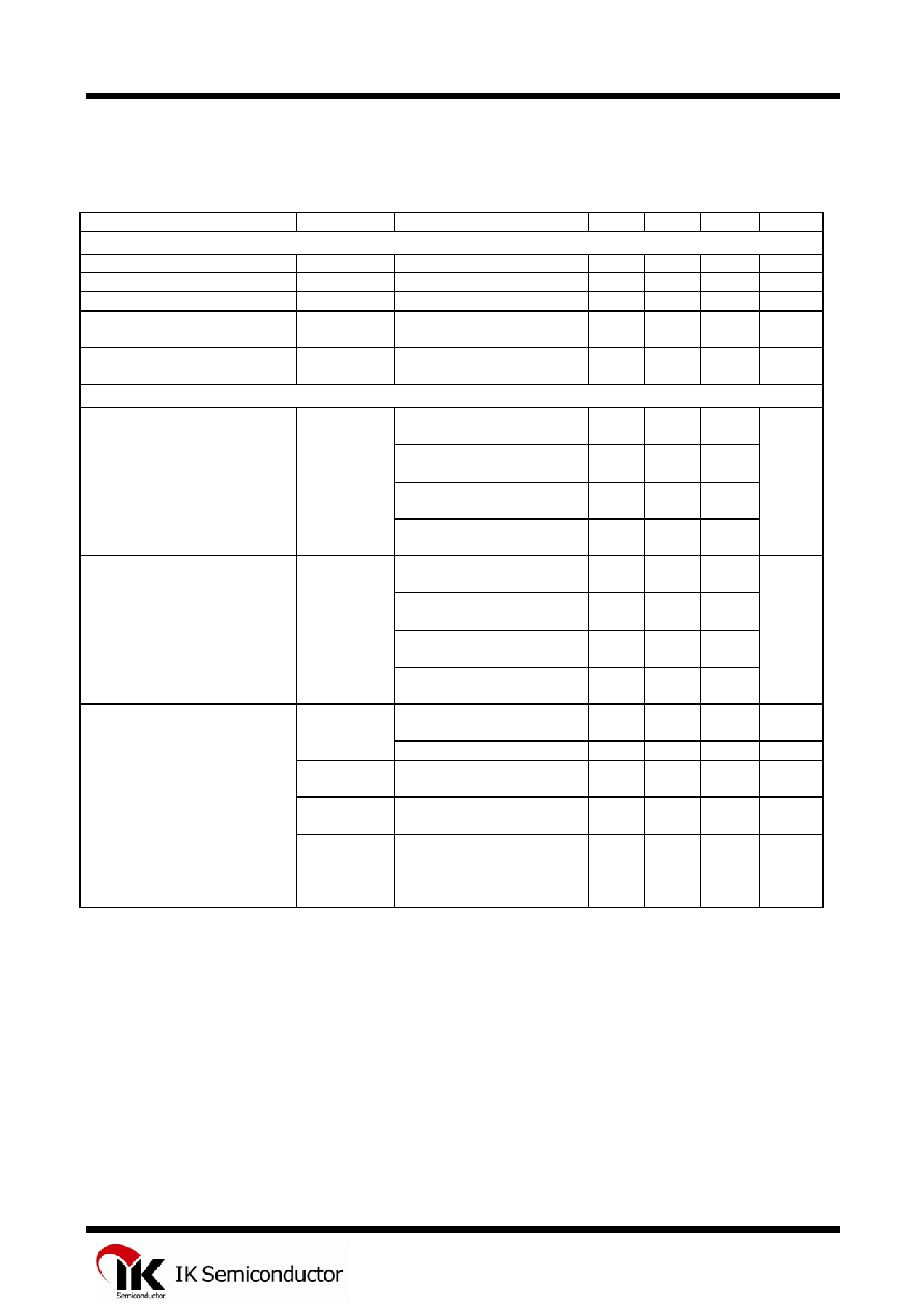
DC ELECTRICAL CHARACTERICTICS
(Unless otherwise specified Vin=13V, Vout connected to V
DD
, Iout=10mA, Cout=100µF, Tj=25
o
C)
Parameter Symbol
Conditions Min
Typ
Max
Units
Voltage regulator
Output Voltage
Vout
6V Vin 24V
4.8
5.0
5.2
V
Voltage Regulation
Reg-Line
6V Vin 16V
30
mV
Load Regulation
Reg-Load
10mA Iout 100mA
50
mV
Dropout Voltage
Vd
Iout=50mA
Iout=100mA
0.5
0.7
V
Quiescent Current
Iq
S1in, S2in, S3in, SWin,
RSin, Din ≠ open
1.0
mA
Logic blokes
High Level Voltage S1out
V
OH
S1in=2 - 5V,
Iload= - 0.5mA
S1in
- 1.2V
V
S2out
S2in=3V,
Iload= - 0.5mA
V
DD
- 0.5V
S3out
S3in=2 - 5V,
Iload= - 0.5mA
V
DD
- 0.5V
S4out
S3in=0.2V
Iload= - 0.1mA
V
DD
- 1.5V
Low Level Voltage S1out
V
OL
S1in=0.2V,
Iload=0.1mA
1.5
V
S2out
S2in= V
DD
-0.2V,
Iload=0.1mA
1.5
S3out
S3in=0.2V,
Iload=0.1mA
1.5
S4out
S3in=2 -5V,
Iload= 0.5mA
0.5
Input Current
S1in, S2in, S3in, RSin
Iin S1in=5V,
S2in=0V,
S3in=5V, Rsin=5V,
0.50
mA
SWin
SWin=5V
3.5
mA
Output Current Din
IDin -
SWin=5V, RSin=0V,
Din=13V, Dout=0V
100 mA
Leakage Current Din
I leakage
SWin=5V, RSin=5V,
Din=13V, Dout=0V
10
µA
Saturation Voltage D
Vsat
SWin=5V, RSin=0V
Dout=0V
Iout=50mA
Iout=100mA
0.5
0.7
V
3
IK31001
AC ELECTRICAL CHARACTERISTICS
(C
L
=15pF, V
DD
= 5 V)
(Unless otherwise specified Vin=13V, Vout connected to V
DD
, Iout=10mA, Cout=100µF, Tj=25
o
C)
Parameter Sumbol
Conditions Min
Typ
Max
Units
Propagation delay
from S1in to S1out
tp
LH
tp
HL
C
L
=100p
65
400
ns
Propagation delay
from S2in to S2out
tp
LH
tp
HL
C
L
=100p
190
720
ns
Propagation delay
from S3in to S3out
tp
LH
tp
HL
C
L
=100p
240
1250
ns
Propagation delay
from S3in to S4out
tp
LH
tp
HL
C
L
=100p
550
65
ns
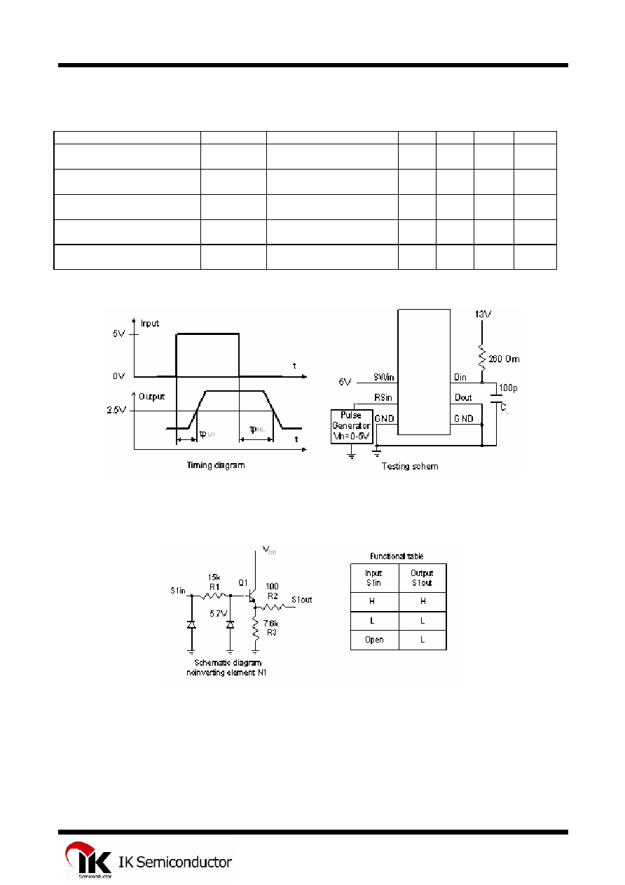
Propagation delay (*1)
from RSin to Din
tp
LH
tp
HL
SWin=5V, Dout=0V,
R
L
=260 Om, C
L
=100p
50
75
ns
*1-See circuit in testing schema
Logical blokes
∑
for MICOM Input
∑
IGN Sensing
∑
TAIL Light Sensing
4