
IN16C554PL/IN16C554TQ
QUAD-UART
ASYNCHRONOUS COMMUNICATIONS ELEMENT
1. General Description
IN16C554 is an enhanced quadruple version of the 16C550 UART (Universal Asynchronous Receiver Transmitter).
Each channel can be put into FIFO mode to relieve the CPU of excessive software overhead. In this mode, internal
FIFOs are activated and 16 bytes plus 3 bit of error data per byte can be stored in both receive and transmit modes.
Each channel performs serial-to-parallel conversion on data characters received from a peripheral device or a
MODEM, and parallel-to-serial conversion on data characters received from the CPU. The CPU can read the complete
status of the UART at any time during the functional operation. The Status information includes the type and condition
of the transfer operations being performed by the UART, as well as any error conditions such as parity, overrun, framing,
and break interrupt.
IN16C554 includes a programmable baud rate generator which is capable of dividing the timing reference clock input
by divisors of 1 to 2
16
-1, and producing a 16x clock for driving the internal transmitter logic. Provisions are also
included to use this clock to drive the receiver logic.
IN16C554 has complete MODEM-control capability and an interrupt system that can be programmed to the user's
requirements, minimizing the computing required to handle the communication links.
2. Features
In the FIFO mode, Each channel's transmitter and receiver is buffered with 16-byte FIFO to reduce the
number of interrupts to CPU.
Adds or deletes standard asynchronous communication bits (start, stop, parity) to or from the serial data.
Holding Register and Shift Register eliminate need for precise synchronization between the CPU and serial
data.
Independently controlled transmit, receive, line status and data interrupts.
Programmable Baud Rate Generators which allow division of any input reference clock by 1 to 2
16
-1 and
generate an internal 16X clock.
Independent receiver clock input
Modem control functions (CTS#, RTS#, DSR#, DTR#, RI#, and DCD#).
Fully programmable serial interface characteristics.
- 5-, 6-, 7-, or 8-bit characters
- Even-, Odd-, or No-Parity bit
- 1-, 1.5-, 2-Stop bit generation. ( Like other general UARTs, IN16C554 checks only one stop bit, no matter
how many they are)
False start bit detection
Generates or Detects Line Break
Internal diagnostic capabilities : Loop-back controls for communications link fault isolation.
Full prioritized interrupt system controls
5
1
IN16C554PL/IN16C554TQ
QUAD-UART
ASYNCHRONOUS COMMUNICATIONS ELEMENT
3. Signal Description
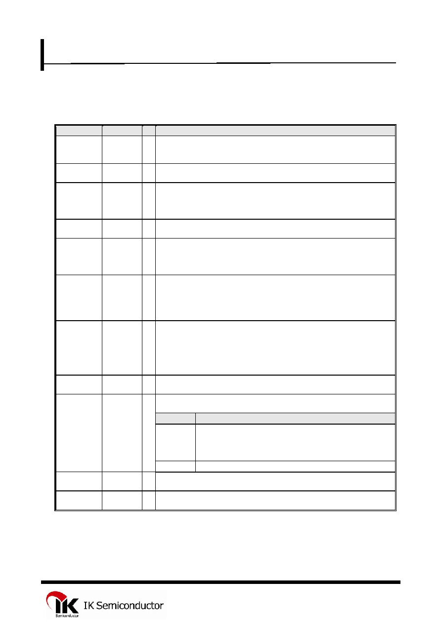
NAME
PIN NO.
I/O
DESCRIPTION
A0
A1
A2
34 (48)
33 (47)
32 (46)
I
Register select pins. A0, A1, and A2 three inputs are used to select the register
of the UART during read and write operations.
CS0#, CS1#
CS2#, CS3#
16,20 (28, 33)
50,54 (68, 73)
I
Chip Select. Each CSx# enables read and write operations to its respective
channel.
CTS0#,
CTS1#
CTS2, CTS3#
11,25 (23, 38)
45,59 (63, 78)
I
Clear to send. CTSx# is a modem status signal. Its status can be known by
reading bit 4 of the modem status register. CTS# does not affect the transmitor
receive operation.
D7~D3,
D2~D0
66~68(15~11)
1~ 5 (9~7)
I/O
Data Bus. Eight data lines with 3-state outputs provide a bidirectional path for data,
control, and status information between the IN16C554 and the CPU. D0 is the LSB.
DCD0#,
DCD1#
DCD2#,
DCD3#
9,27 (19, 42)
43, 61 (59, 2)
I
Data Carrier Detect. A low on DCDx# indicates the carrier has been
detected by the modem. Its condition can be known by reading bit 7 of
the modem status register.
DSR0#,
DSR1#
DSR2#,
DSR3#
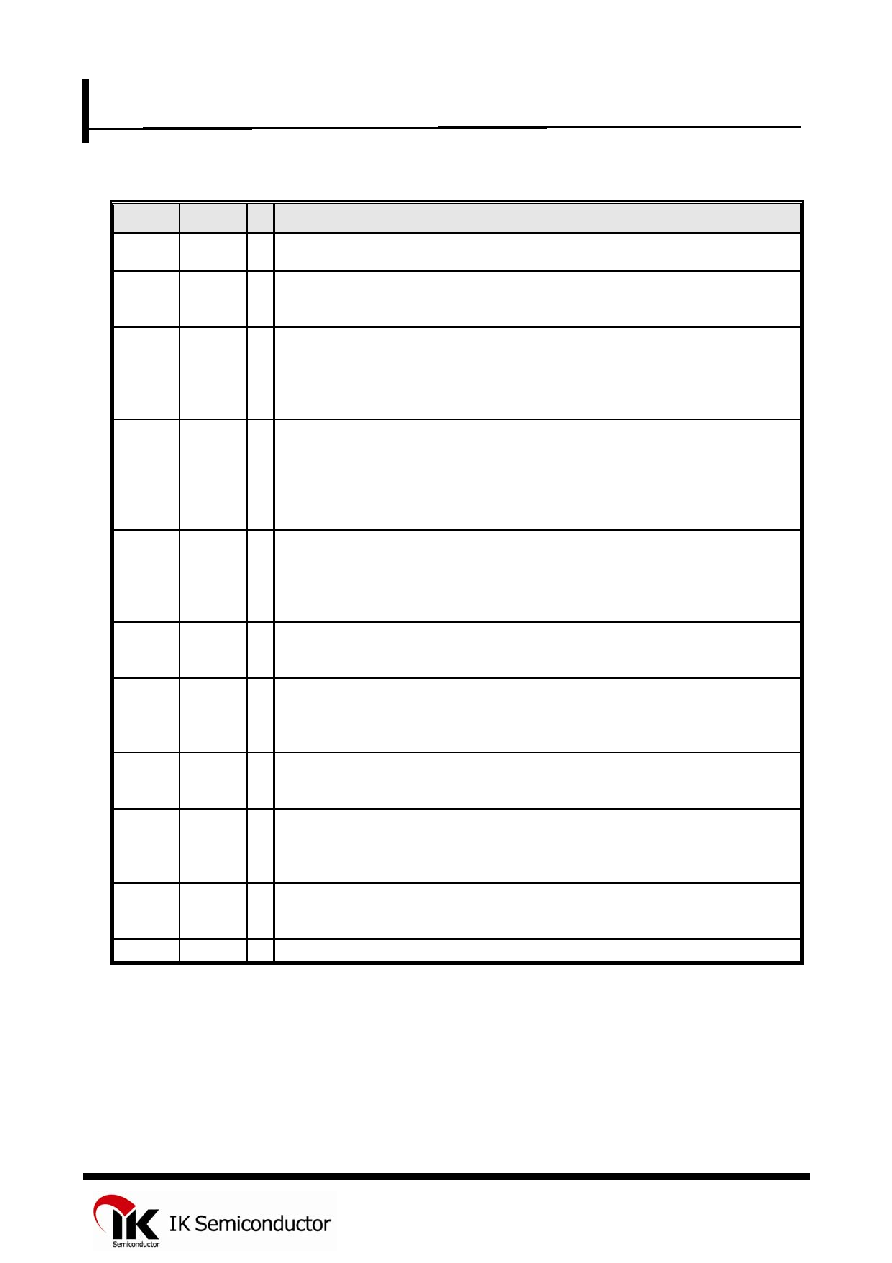
10,26 (22, 39)
44,60 (62, 79)
I
Data set ready. DSRx# is a modem status signal. The condition of DSRx# can
be checked by reading the Bit 5 of the modem status register. DSR# does not
affect the transmit or receive operation.
DTR0#,
DTR1#
DTR2#,
DTR3#
12, 24(24, 37)
46, 58(64,77)
O
Data Terminal Ready. DTRx# is an output that indicates to a modem or data set that
the UART is ready to establish communications. Setting the DTR bit of the modem
control register activates it. DTRx# is placed in inactive state either as a result of the
master reset during loop mode operation or clearing bit 0 of the modem control
register.
GND
6, 23 (16,36)
40, 57 (56,76)
signal and power ground
Interrupt normal. INTN# in conjunction with bit 3 of the modem status register
and affects operation of the four interrupts (INT0~INT3).
INTN#
Operation Of Interrupts
Low or
Float
Interrupts are enabled according to the state of OUT2 (MCR bit 3).
When the MCR bit 3 is cleared, the 3-state interrupt output of that
UART is in the high Z state. When MCR bit 3 is set, the interrupt
output of the UART is enabled.
INTN#
65 (6)
I
High
Interrupts are always activated.
INT0, INT1
INT2, INT3
15,21(27,34)
19,55(67,74)
External interrupt output. When activated, INTx output informs CPU that UART has
an interrupt to be serviced.
IOR#
52 (70)
I
Read strobe. A low level on IOR# transfers the contents of the IN16C554 data bus to
the external CPU bus.
5
2
IN16C554PL/IN16C554TQ
QUAD-UART
ASYNCHRONOUS COMMUNICATIONS ELEMENT
NAME
PIN NO. I/O
DESCRIPTION
IOW#
18 (31)
I
Write strobe. IOW# allows the CPU to write into the selected address by the address register.
RESET
37 (53)
I
Master reset. When active, RESET clears most UART registers and sets the state of various
signals. The transmitter output and he receiver input is disabled during reset time.
RI0#,
RI1#
RI2#,
RI3#
8, 28
(18,43)
42, 62 (58,
3)
I
Ring detect indicator. A low on Rix# indicates the modem has received a ring signal from the
telephone line. The condition of this signal can be
checked by reading bit 6 of the modem status register.
RTS0#,
RTS1#
RTS2#,
RTS3#
14, 22
(26,35)
48, 56
(66,75)
O
Request to Send. When active, RTSx# informs the modem or data set that the UART is ready
to receive data. Writing a 1 in the modem control register sets this bit to a low state. After
reset, this terminal is set high. These terminals have no affect on the transmit or receive
operation.
RXD0,
RXD1
RXD2,
RXD3
7, 29 (17,
44)
41, 63 (57,
4)
I
Serial Input. RXDx is a serial data input from a connected communications device. During
loopback mode, the RXDx input is disabled from external connection and connected to the
TXDx output internally.
RXRDY
#
38 (54)
O
Receive ready. RXRDY# goes low when the receive FIFO is full. It can be used as a single
transfer or multi transfer.
TXD0,
TXD1
TXD2,
TXD3
17, 19
(29,32)
51, 53
(69,72)
O
Transmit output. TXDx is a composite serial data output that is connected to a
communications device. TXD1, TXD2, TXD3, and TXD4 are set to the high state as a result
of reset.
TXRDY
#
39 (55)
O
Transmit Ready. TXRDY# goes low when the transmit FIFO is full. It can be used as a single
transfer of multi transfer.
VCC
13, 30 (5,
25)
47, 64
(45,65)
Power supply.
XTAL1
35 (50)
I
Crystal input 1 or external clock input. A crystal can be connected to XTAL1 and XTAL2 to
utilize the internal oscillator circuit. An external clock can be connected to drive the internal
clock circuits.
XTAL2
36 (51)
O
Crystal output 2 or buffered clock output.
At the PIN NO, the number outside the parenthesis means the pin number of the IN16C554PL, and the number inside the parenthesis
means the pin number of the IN16C554TQ.
5
3
IN16C554PL/IN16C554TQ
QUAD-UART
ASYNCHRONOUS COMMUNICATIONS ELEMENT
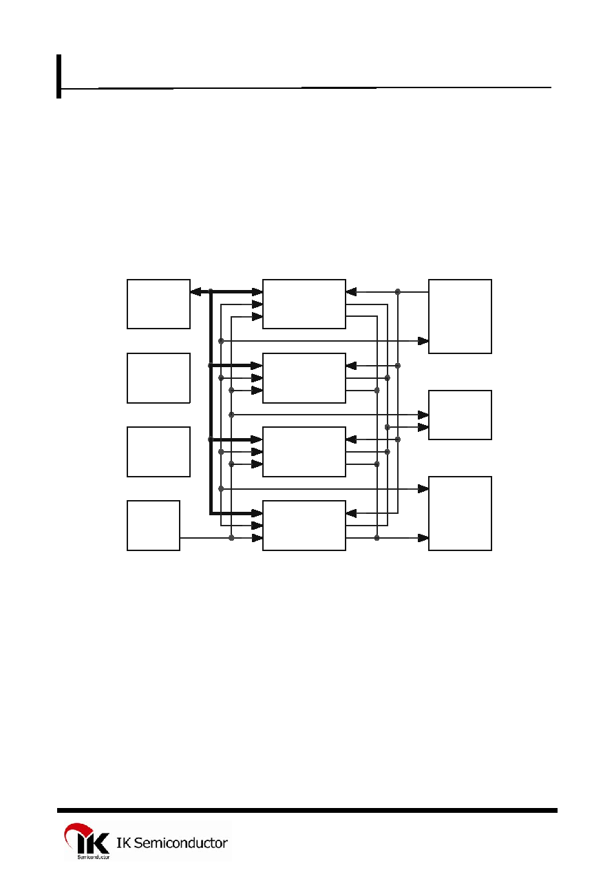
4. Functional Block Diagram
Transmit
Control
Logic
DTRx#
1 6 C 5 5 0
Logic
1 6 C 5 5 0
Logic
XTAL2
RIx#
D7-D0
DCDx#
C o n t r o l
Logic
A2-A0
D A T A
BUS
Clock
Circuit
1 6 C 5 5 0
Logic
RXRDY#
RTSx#
TXRDY#
CTSx#
CSx#
XTAL1
DSRx#
IOR#
1 6 C 5 5 0
Logic
RXDx
Modem
Control
Logic
IOW#
RESET
Receive
Control
Logic
I n t e r r u p t
Logic
INTx
TXDx
5
4
IN16C554PL/IN16C554TQ
QUAD-UART
ASYNCHRONOUS COMMUNICATIONS ELEMENT
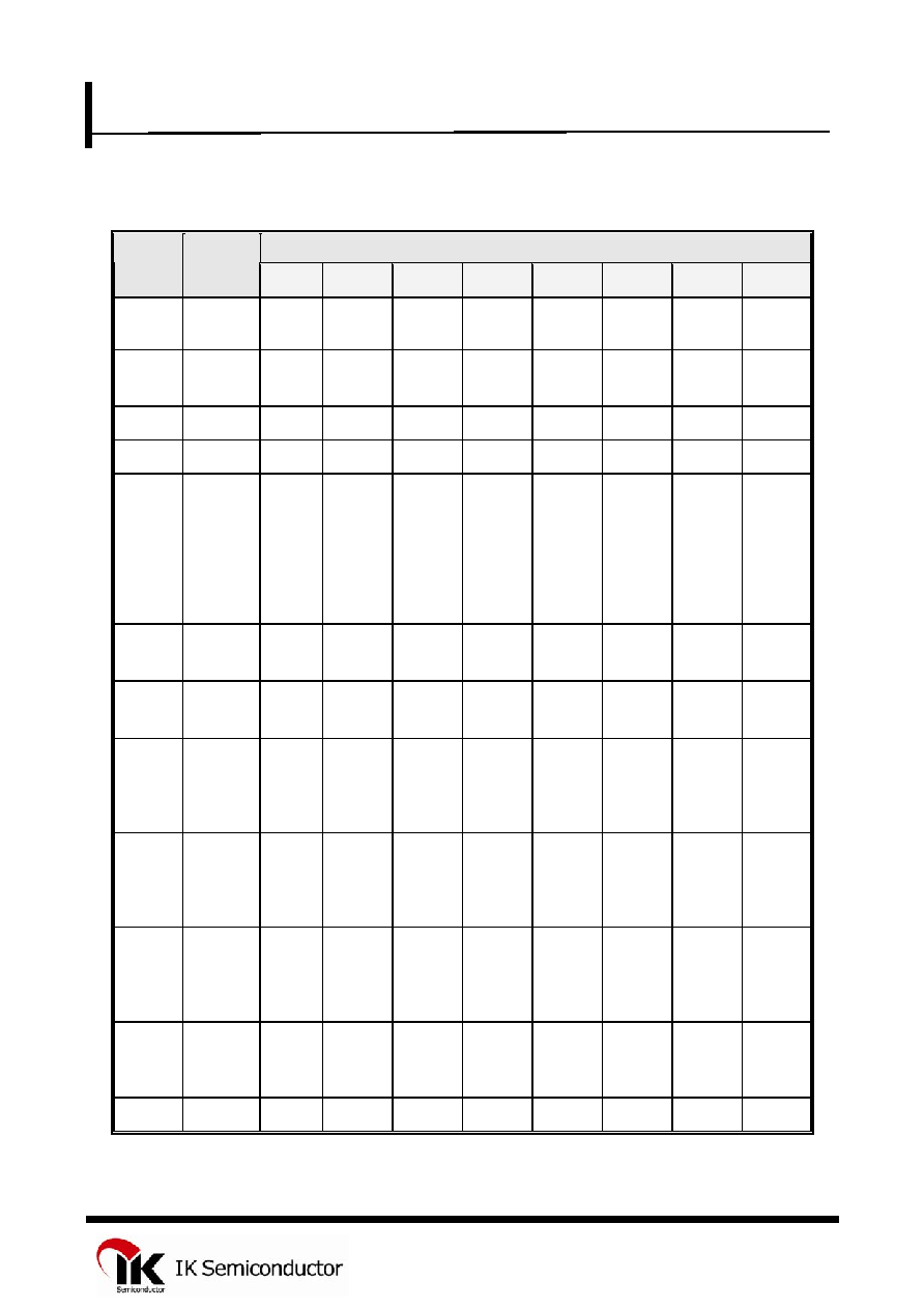
5. Register Description
REGISTER ADDRESS
ADDRESS
REGISTER
MNEMONIC
BIT 7
BIT 6
BIT 5
BIT 4
BIT 3
BIT 2
BIT 1
BIT 0
0 RBR
(read only)
Data bit
7 (MSB)
Data bit 6
Data bit 5
Data bit 4
Data bit 3
Data bit 2
Data bit 1
Data bit 0
(LSB)
0
THR
(write only)
Data bit
7
Data bit 6
Data bit 5
Data bit 4
Data bit 3
Data bit 2
Data bit 1
Data bit 0
0
DLL
Bit 7
Bit 6
Bit 5
Bit 4
Bit 3
Bit 2
Bit 1
Bit 0
1
DLM
Bit 15
Bit 14
Bit 13
Bit 12
Bit 11
Bit 10
Bit 9
Bit 8
1 IER 0
0 0 0
(EDSSI)
Enable
modem
status
interrupt
(ERLSI)
Enable
receiver
line status
interrupt
(ETBEI)
Enable
Transmitte
r
Holding
register
empty
interrupt
(ERBI)
Enable
received
data
available
interrupt
2 FCR
(write only)
Receiver
Trigger
(MSB)
Receiver
Trigger
(LSB)
Reserved Reserved DMA
mode
select
Transmit
FIFO reset
Receiver
FIFO reset
FIFO
enable
2
IIR
(read only)
FIFOs
Enabled
FIFOs
Enabled
0 0 Interrupt
ID Bit (3)
Interrupt
ID Bit (2)
Interrupt
ID Bit (1)
0 if
interrupt
pending
3 LCR
(DLAB)
Divisor
latch
access
bit
Set break
Stick
Parity
(EPS)
Even
parity
select
(PEN)
Parity
Enable
(STB)
Number of
Stop bits
(WLSB1)
Word
length
select bit 1
(WLSB0)
Word
length
select bit 0
4 MCR
0
0 0
Loop OUT2
Enable
external
interrupt
(INT)
Reserved (RTS)
Request to
Send
(DTR)
Data
terminal
ready
5 LSR
Error in
receiver
FIFO
(TEMT)
Transmitte
r registers
empty
(THRE)
Transmitte
r holding
register
empty
(BI)
Break
interrupt
(FE)
Framing
Error
(PE)
Parity
Error
(OE)
Overrun
error
(DR)
Data ready
6 MSR
(DCD)
Data
carrier
detect
(RI)
Ring
indicator
(DSR)
Data set
Ready
(CTS)
Clear to
Send
(DCD)
Delta data
carrier
detect
(TERI)
Trailing
Edge ring
indicator
(DSR)
Delta data
set ready
(CTS)
Delta clear
to send
7
SCR
Bit 7
Bit 6
Bit 5
Bit 4
Bit 3
Bit 2
Bit 1
Bit 0
DLAB = 1
This bit is always in a low state when FIFO is disabled.
5
5
IN16C554PL/IN16C554TQ
QUAD-UART
ASYNCHRONOUS COMMUNICATIONS ELEMENT
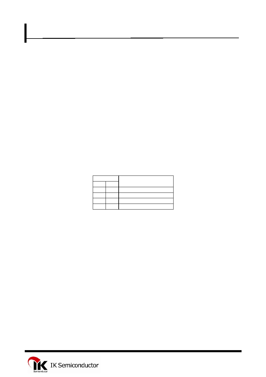
5.1. FIFO control register(FCR)
The FCR is a write-only register at the same address as the IIR. FCR enables FIFO, sets the trigger level of the
receiver FIFO, and selects the type of DMA signaling.
Bit 0 : FCR0 enables transmit and receiver FIFOs. All bytes in both FIFOs can be cleared by clearing this bit.
Data is cleared automatically from the FIFOs when changing from the FIFO mode to the 16C550 mode and
vice versa. Programming of other FCR bits is enabled by setting this bit.
Bit 1 : When set, FCR1 clears all bytes in the receiver FIFO and resets its counter. This does not clear the shift
register.
Bit 2 : When set, FRC2 clears all bytes in the transmitter FIFO and resets its counter. This does not clear the
shift register.
Bit 3 : When set, FRC3 changes RXRDY# and TXRDY# from mode 0 to mode 1 if FCR0 is set.
Bit 4, 5 : Reserved for the future use.
Bit 6, 7 : FCR6 and FCR7 set the trigger level for the receiver FIFO interrupt. (see Table 1).
Table 1. Receiver FIFO Trigger Level
BIT
7 6
Receiver FIFO
Trigger Level
0 0
01
0 1
04
1 0
08
1 1
14
* FIFO interrupt mode operation
The following receiver status occurs when the receiver FIFO and receiver interrupts are enabled.
1.
LSR0 is set when a character is transferred from the shift register to the receiver FIFO. When the FIFO is
empty, it is reset.
2.
Receiver line status interrupt(IIR = 06) has higher priority than the receive data available interrupt(IIR = 04).
3.
Receive data available interrupt is issued to the CPU when the programmed trigger level is reached by the
FIFO. As soon as the FIFO drops below its programmed trigger level, it is cleared.
4.
Receive data available indicator(IIR=04) also occurs when the FIFO reaches its trigger level. It is cleared
when the FIFO drops below the programmed trigger level.
The following receiver FIFO character time-out status occurs when receiver FIFO and receiver interrupts are enabled.
1.
When the following conditions exist, a FIFO character time-out interrupt occurs.
a.
Minimum of one character in FIFO.
b.
Last received serial character is longer than four continuous previous character times ago. (If two stop bits
are programmed, the second one is included in the time delay. Only the first stop bit is checked by the
UART.)
c.
The last CPU of the FIFO read is more than four continuous character times earlier.
2.
By using the XTAL1 input for a clock signal, the character times can be calculated. The delay is proportional to
the baud rate.
5
6

IN16C554PL/IN16C554TQ
QUAD-UART
ASYNCHRONOUS COMMUNICATIONS ELEMENT
3.
The time-out timer is reset after the CPU reads the receiver FIFO or after a new character is received. This occurs
when there has been no time-out interrupt.
4.
A time-out interrupt is cleared and the timer is reset when the CPU reads a character from the receiver FIFO.
Transmit interrupts occurs as follows when the transmitter and transmit FIFO interrupts are enabled (FCR=0, IER=1).
1.
When the transmitter FIFO is empty, the transmitter holding register interrupt (IIR=02) occurs. The interrupt is
cleared when the transmitter holding register is written to or the IIR is read. 1 to 16 characters can be written to
the transmit FIFO when servicing this interrupt.
2.
The transmitter FIFO empty indicators are delayed one character time minus the last stop bit time whenever the
following occurs.
THRE=1, and there has not been a minimum of two bytes at the same time in transmit FIFO since the last
THRE=1. The first transmitter interrupt after changing FCR0 is immediate, however, assuming it is enabled.
Receiver FIFO trigger level and character time-out interrupts have the same priority as the receive data available
interrupt.
The transmitter holding register empty interrupt has the same priority as the transmitter FIFO empty interrupt.
5.2. Line Control Register
The format of the data character is controlled by the LCR.
Bit 0, 1 : LCR0 and LCR1 are word length select bits. (see Figure 1)
Bit 2 : LCR2 is the stop bit select bit. The receiver always checks for one stop bit.
Bit 3 : LCR3 is the parity enable bit. When LCR3 is set, a parity bit is generated and checked.
Bit 4 : LCR4 is the even parity select bit. When LCR3 and this bit is set, even parity is generated and checked.
When LCR3 is set and this bit is cleared, odd parity is selected.
Bit 5 : LCR5 is the stick parity select bit. When LCR3 and this bit is set, the transmission and the reception of
a parity bit is forced to an opposite state from the value of LCR4. Clearing this bit disenables the stick parity.
Bit 6 : LCR6 is a break control bit. When this bit is set, the serial outputs TXDxs are forced to `0'. The break
control bit acts only on the serial output and does not affect the transmitter logic. If the following sequence is
used, no invalid characters are transmitted because of the break.
1.
Load a zero byte in response to the transmitter holding register empty(THRE) status indicator.
2.
The next THRE signal in the response of the set the break.
3.
Wait for the transmitter to be idle, when transmitter empty status signal is set (TEMT=1) and then clear
the break, and start the normal transmission.
Bit 7 : LCR7 is the divisor latch access bit(DLAB). This bit must be set to access the divisor latches DLL and
DLM of the baud rate generator during a read or write operation. LCR7 must be cleared to access the
Receiver Buffer Register, the Transmitter Holding Register, or the Interrupt Enable Register.
5
7
IN16C554PL/IN16C554TQ
QUAD-UART
ASYNCHRONOUS COMMUNICATIONS ELEMENT
0 = Break Disabled
2 Stop Bits if 6,7,8 Data Bits Selected
0
LCR
1 = Break Enabled
Access Bit
0 = Parity Disabled
LCR
Word Length
Select
0 = Access Receiver Buffer
0 0 = 5 Data Bits
Parity Enable
Stop Bit
1 = Access Divisor Latches
0
Select
0
LCR
0 = 1 Stop Bit
0
LCR
1 0 = 7 Data Bits
0
0
1 1 = 8 Data Bits
LCR
0
0 1 = 6 Data Bits
0 = Stick Parity Disabled
0 = Odd Parity
0
Even Parity
1 = Even Parity
Stick Parity
Break Control
1 = 1.5 Stop Bits if 5 Data Bits Selected
1 = Parity Enabled
LCR
LCR
1 = Stick Parity Enabled
LCR
Divisor Latch
Figure 1. Line Control Register
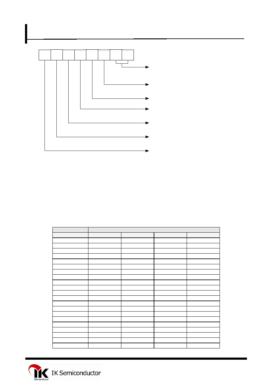
* Programmable Baud Generator
The UART contains a programmable Baud Generator that is capable of taking any clock input from DC to 14.7456MHz and dividing it by any
divisor from 2 to 2
16
-1. 4MHz is the highest clock input recommended when the divisor = 1. The output frequency of the baud generator is 16 x
baud [divisor # = (frequency input)/(baud rate X 16)]. Two 8-bit latches store the divisor in a 16-bit binary format. These Divisor Latches must be
loaded during initialization to ensure proper operation of the Baud Generator. (see Table 2.)
Table 2. Baud rates
This table provides decimal divisors to use with crystal frequencies of 1.8432MHz, 3.6864MHz, 7.3728MHz and 14.7456MHz. For baud rates
of 38400 and below, the error obtained is minimal. The accuracy of the desired baud rate is dependent on the frequency of the crystal. It is not
recommended using a divisor of zero.
Decimal divisor to generate 16x Clock
Desired baud rate
1.8432MHz
3.6864MHz
7.3728MHz
14.7456MHz
50 2304 4608 9216 18432
75 1536 3072 6144 12288
134.5 857 1714 3428 6856
150 768 1536 3072 6144
300 384 768
1536
3072
600 192 384 768 1536
1200 96 192 384 768
1800 64 128 256 512
2000 58 116 232 464
2400 48 96 192 384
3600 32 64 128 256
4800 24 48 96 192
7200 16 32 64 128
9600 12 24 48 96
19.2K 6 12 24 48
38.4K 3 6 12 24
57.6K
2 4 8 16
115.2K
1 2 4 8
230.4K
- 1 2 4
460.8K - - 1 2
921.6K
- - - 1
5
8

IN16C554PL/IN16C554TQ
QUAD-UART
ASYNCHRONOUS COMMUNICATIONS ELEMENT
5.3. Line Status Register
This register provides status information to the CPU concerning the data transfer.
Bit 0 : Data Ready(DR) indicator. Bit 0 is set to a logic 1 whenever a complete incoming character has been received and transferred into
the Receiver Buffer Register or the FIFO. This bit is cleared by reading all of the data in the Receiver Buffer Register of the FIFO.
Bit 1 : Overrun Error(OE) indicator. Bit 1 indicates that data in the Receiver Buffer Register was not read by the CPU before the next
character was transferred into the Receiver Buffer Register, thereby destroying the previous character. This bit is set to a logic 1 when
overrun occurs and cleared whenever the CPU reads the contents of the Line Status Register. If the FIFO mode data continues to fill the
FIFO beyond the trigger level, an overrun error will occur only after the FIFO is full and the next character has been completely received
in the shift register. OE is indicated to the CPU as soon as it happens. The character in the shift register is overwritten, but it is not
transferred to the FIFO.
Bit 2 : Parity Error indicator. Bit 2 is set to a logic 1 upon detection of a parity error and is reset to a logic 0 whenever CPU reads the
contents of the Line Status Register. In the FIFO mode, this error is revealed to CPU when its associated character is at the top of the
FIFO.
Bit 3 : Framing Error indicator. Bit 3 indicates that the received character did not have a valid stop bit. This bit is set to a logic 1
whenever the stop bit following the last data bit or parity bit is detected as a logic 0 bit. It is reset to a logic 0 whenever CPU reads the
contents of the Line Status Register. In the FIFO mode, this error is revealed to CPU when its associated character is at the top of the
FIFO. When this error has been detected, CPU assumes it due to a next start bit, so it samples this start bit twice and the take the data.
Bit 4 : Break Interrupt indicator. Bit 4 is set to a logic 1 when the received data input is held in the spacing state for longer than a full
word transmission time (start bit + data bits + parity bit + stop bits). The BI indicator is reset to a logic 0 whenever the CPU reads the
contents of the Line Status Register. In the FIFO mode, this error is revealed to CPU when its associated character is at the top of the
FIFO. When break occurs, only one zero character is loaded into the FIFO. The next character transfer is enabled after SIN goes HIGH
and receives the next start bit.
Bit 5 : Transmitter holding register empty(THRE) indicator. Bit 5 indicates that the UART is ready to take a new character for
transmission. In addition, this bit causes the UART to issue an interrupt to the CPU when the Transmit Holding Register Empty interrupt
enable is set to HIGH. This bit is set to a logic 1 when a character is transferred from the Transmitter Holding Register into the
Transmitter shift register. And it is reset to a logic 0 when the CPU transfers data to the Transmitter Holding Register. In the FIFO mode,
this bit is set to a logic 1 when the XMIT FIFO is empty, and is reset to a logic 0 when at least one byte is written to the XMIT FIFO.
Bit 6 : Transmitter Empty indicator. This bit is set when the Transmitter Holding Register and Transmitter Shift Register are both empty,
and reset to a logic 0 when the THR contains a data character. In the FIFO mode, it is set to a logic 1 when the both the Transmitter FIFO
and the Transmitter Shift Register are empty.
Bit 7 : In the 16C550 mode, this bit is a 0. In the FIFO mode it is set to a logic 1 when it contains at least one error such as parity error,
framing error or break error. This bit is reset to a logic 0 when the CPU reads the Line Status Register and there exists no error.
5
9

IN16C554PL/IN16C554TQ
QUAD-UART
ASYNCHRONOUS COMMUNICATIONS ELEMENT
5.4. Interrupt Identification Register
In order to provide minimum software overhead during data transfer, the UART prioritizes interrupts into 4 levels and record these in the Interrupt
Identification Register. The four levels of interrupt conditions are, in order of priority:
Receiver Line Status
Received Data Ready
Transmitter Holding Register Empty
MODEM Status
When the CPU accesses the IIR, the UART freezes all interrupts and indicates the highest priority pending interrupt to the CPU. While this CPU
access is occurring, the UART records new interrupts, but does not change its current indication until the access is complete.
Bit 0 : This bit can be used in a prioritized interrupt environment to indicate whether an interrupt is pending. When bit 0 is a logic 0, an interrupt is
pending and the IIR contents may be used as a pointer to the appropriate interrupt service routine. When bit 0 is a logic 1, no interrupt is
pending.
Bit 1, 2 : These two bits of the IIR are used to identify the highest priority interrupt pending as indicated in Table 3.
Bit 3 : In the 16C550 mode, this bit is 0. In the FIFO mode, this bit is set along with bit 2 when a time-out interrupt is pending.
Bit 4, 5 : These two bits are always logic 0.
Bit 6, 7 : These two bits are set whenever FCR0 is a logic 1.
Table 3. Interrupt Control Function
FIFO
mode
only
Interrupt Identification
Register
Interrupt set / reset Function
Bit 3
Bit 2
Bit 1
Bit 0
Priority
Level
Interrupt
Type
Interrupt Source
Interrupt Reset Control
0 0 0 1 - -
-
-
0 1 1 0 1 Receiver
Line Status
OE, PE, FE, BI
Reading the LSR
0 1 0 0 2 Receiver
Data
Available
Receiver Data Available or Trigger
level reached
Reading the RBR
or the FIFO drops below the
trigger level
1 1 0 0 2 Character
Timeout
Indication
No character has been removed
since the last transfer and there was
no transfer at the FIFO during the 4
character time.
Reading the RBR
0 0 1 0 3 Transmitter
Holding
Register
Empty
Transmitter Holding Register
Empty
Reading the IIR (if source
of the interrupt ) or writing the
THR
0 0 0 0 4 Modem
Status
CTS, DSR, RI, DCD
Reading the MSR
5
10

IN16C554PL/IN16C554TQ
QUAD-UART
ASYNCHRONOUS COMMUNICATIONS ELEMENT
5.5. Interrupt Enable Register
The IER independently enables the four serial channel interrupt sources that activate the interrupt( INT0, INT1, INT2, INT3) output. All interrupts
are disabled by clearing IER0-IER3 of the IER. Interrupts are enabled by setting the appropriate bits of the IER. Disabling the interrupt system
inhibits the IIR and the active high interrupt output. All other system functions operate in their normal manner, including the setting of the LSR and
MSR. The contents of the IER are described in the following bulleted list.
Bit 0 : When IER0 is set, IER0 enables the received data available interrupt and the timeout interrupts in the FIFO mode.
Bit 1 : When IER1 is set, the transmitter holding register empty interrupt is enabled.
Bit 2 : When IER2 is set, the receiver line status interrupt is enabled.
Bit 3 : When IER3 is set, the modem status interrupt is enabled.
Bit 4~7 : These bits are cleared.
5.6. Modem Control Register
The MCR controls the interface with the modem or data set as described in Figure 2. MCR can be written and read. The RTS# and DTR# outputs are
directly controlled by their control bits in this register. A high input asserts a low signal at the output terminals. MCR bits 0-4 are shown as follows.
Bit 0 : When MCR0 is set, the DTR# output is forced low. When MCR0 is cleared, the DTR# output is forced high. The DTR# output of
the serial channel may be input into an inverting line driver in order to obtain the proper polarity input at the modem or data set.
Bit 1 : When MCR1 is set, the RTS# output is forced to 0. When MCR1 is cleared, the RTS# output is forced high. The DTR# output of
the serial channel may be input into an inverting line driver in order to obtain the proper polarity input at the modem or data set.
Bit 2 : MCR2 has no affect on operation.
Bit 3 : When MCR3 is set, the external serial channel interrupt is enabled.
Bit 4 : MCR4 provides a local loopback feature for diagnostic testing of the channel. When MCR4 is set, serial output TXDx is set to the
high state and SIN is disconnected. The output of the TSR is looped back into the RSR input. The four modem control inputs (CTS#,
DSR#, DCD#, RI#) are disconnected. The modem control outputs (DTR#, RTS#) are internally connected to the four modem control
inputs. The modem control output terminals are forced to their inactive state on the IN16C554. In the diagnostic mode, data transmitted is
immediately received. This allows the processor to verify the transmit and receive data path of the selected serial channel. Interrupt
control is fully operational; however, interrupts are generated by controlling the lower four MCR bits internally. Interrupts are not
generated by activity on the external terminals represented by those four bits.
Bit 5~7 : These bits are permanently cleared.
5
11

IN16C554PL/IN16C554TQ
QUAD-UART
ASYNCHRONOUS COMMUNICATIONS ELEMENT
5.7. Modem Status Register
The MSR provides the CPU with status of the modem input lines for the modem or peripheral devices. The MSR allows the CPU to read the serial
channel modem signal inputs by accessing the data bus interface of the UART. It also reads the current status of four bits of the MSR that indicate
whether the modem inputs have changed since the last reading of the MSR. The delta status bits are set when a control input from the modem changes
states and are cleared when the CPU reads the MSR. The contents of the MSR are shown as follows.
Bit 0 : Delta Clear to Send(DCTS) indicator. DCTS indicates that the CTS# input to the serial channel has changed state since it was last
read by the CPU.
Bit 1 : Delta Data Set Ready(DDSR) indicator. DDSR indicates that the DSR# input to the serial channel has changed state since it was
last read by the CPU.
Bit 2 : Trailing Edge of Ring Indicator(TERI) indicator. TERI indicates that the RI# input to the serial channel has changed states from
low to high since the last time it was read by the CPU. High to low transitions on RI do not activate TERI.
Bit 3 : Delta Data Carrier Detect(DDCD) indicator. DDCD indicates that the DCD# input to the serial channel has changed state since it
was last read by the CPU.
* note : An interrupt is generated whenever the bit0~3 of the MSR is set to a logic 1.
Bit 4 : Clear to Send bit. CTS is the complement of the CTS# input from the modem indicating to the serial channel that the modem is
ready to provice received data from the serial channel receiver circuitry. When the channel is in the loop mode, MSR4 reflects the value
of RTS in the MCR.
Bit 5 : Data Set Ready bit. DSR is the complement of the DSR# input from the modem to the serial channel that indicates that the modem
is ready to provide received data from the serial channel receiver circuitry. When the channel is in the loop mode, MSR5 reflects the
value of DTR in the MCR.
Bit 6 : Ring indicator bit. RI is the complement of the Rix# inputs. When the channel is in the loop mode, MSR6 reflects the value of
OUT1# in the MCR.
Bit 7 : Data Carrier Detect bit. Data carrier detect indicates the status of the data carrier detect input. When the channel is In the loop
mode, MSR7 reflects the value of OUT2# in the MCR.
5.8. Scratch Register
This 8-bit read/write register has no affect on either channel of the UART. It is intended to be used by the programmer to hold data temporarily.
5
12
IN16C554PL/IN16C554TQ
QUAD-UART
ASYNCHRONOUS COMMUNICATIONS ELEMENT
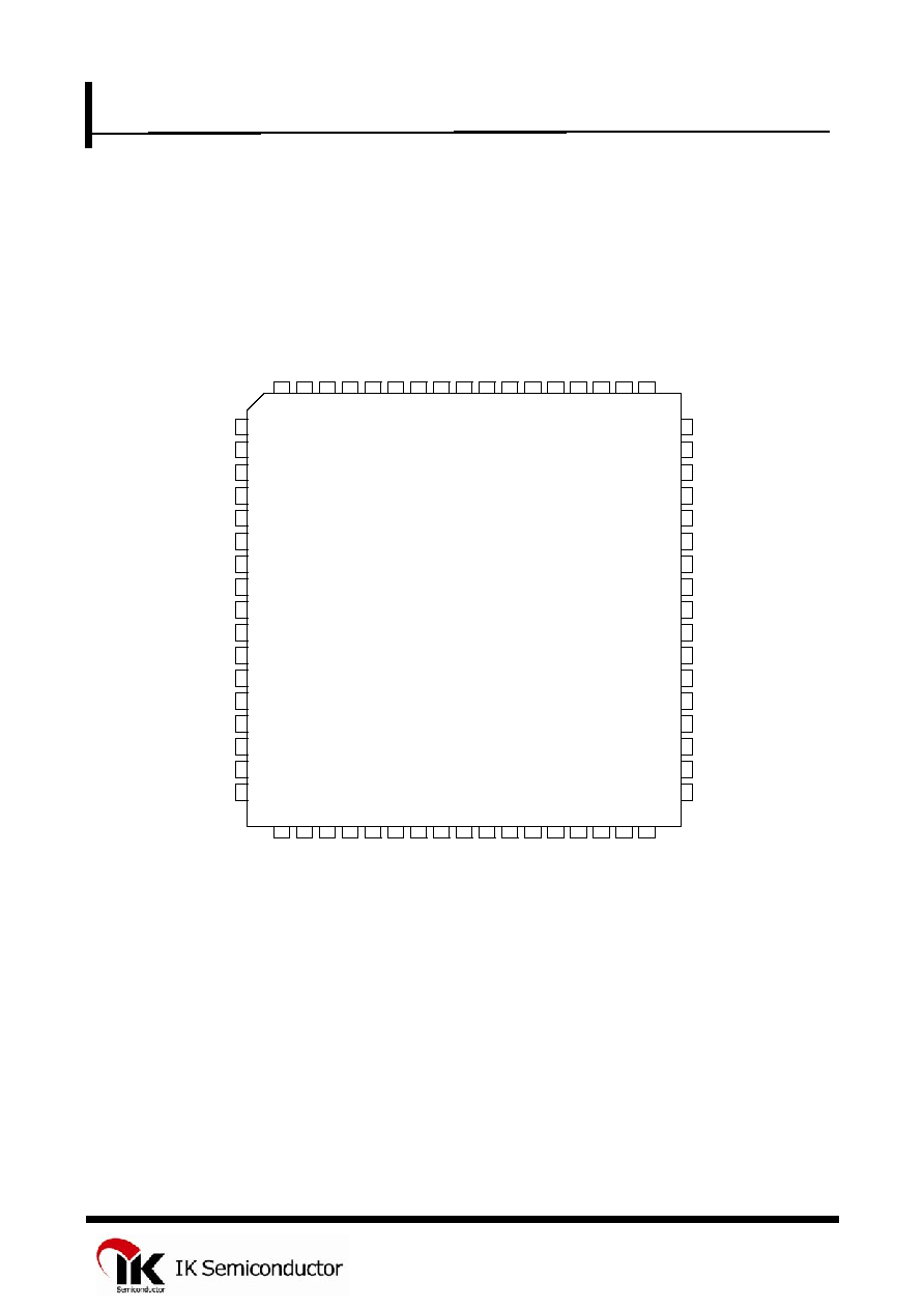
6.
Package Diagram
IN16C554PL PACKAGE (Top)
DSR3#
DTR0#
33
CS2#
50
INT3
VCC
32
TXRDY#
57
49
47
RTS0#
31
VCC
GND
56
48
46
CS3#
INT0
30
DTR3#
DTR2#
RXD2
55
45
21
D1
29
CTS2#
RI2#
54
44
20
D0
28
INT2
DSR2#
VCC
DCD2#
43
19
DSR0#
D5
27
8
DCD3#
RXD3
NC - No internal connection
42
18
D4
3
RTS2#
26
DCD0#
RI3#
60
41
15
TXD1
40
D3
2
RI1#
25
7
RI0#
D6
14
CS1#
39
D2
17
1
RXD1
24
6
RXD0
A0
13
INT1
38
16
68
CS0#
DTR1#
VCC
23
5
64
XTAL1
12
RTS3#
RTS1#
GND
67
TXD0
CTS1#
NC
22
4
63
XTAL2
GND
11
GND
37
66
DSR1#
A2
62
RESET
10
CTS3#
TXD3
53
36
DCD1#
A1
61
IOW#
59
IOR#
D7
52
CTS0#
35
34
65
9
RXRDY#
58
TXD2
INTN#
51
5
13

IN16C554PL/IN16C554TQ
QUAD-UART
ASYNCHRONOUS COMMUNICATIONS ELEMENT
IN16C554TQ PACKAGE (Top)
D5
TXD2
DCD2
#
75
DSR3#
55
40
22
34
69
31
RXD2
4
NC
INTN#
71
1 2
30
73
41
20
A2
32
DSR2#
14
27
44
79
70
GND
50
62
DSR0#
CTS1#
33
NC
56
43
39
21
NC
D4
GND
RXD0
DSR1#
NC
TXRDY#
NC
76
7
RXD1
NC
IOR#
49
10
47
INT0
64
NC - No internal connection
66
RI1
#
NC
RI3
#
NC
25
35
GND
NC
63
17
CS1#
77
80
RTS0#
NC
TXD1
13
D7
RTS1#
29
D2
DTR2#
36
60
INT1
42
8
CTS3#
51
D6
INT3
65
38
53
VCC
D3
D1
TXD0
45
16
XTAL1
11
RTS3#
26
CS3#
NC
IOW#
24
CS0#
78
6
68
67
D0
DCD3
#
57
VCC
DTR0#
15
VCC
RI2
#
59
VCC
GND
XTAL2
RXD3
A1
54
37
48
CS2#
NC
18
3
CTS2#
28
TXD3
58
DTR1#
19
23
RTS2#
74
DTR3#
12
61
9
5
DCD1
#
CTS0#
INT2
72
A0
RESET
RXRDY#
RI0
#
46
NC
52
DCD0
#
5
14
IN16C554PL/IN16C554TQ
QUAD-UART
ASYNCHRONOUS COMMUNICATIONS ELEMENT
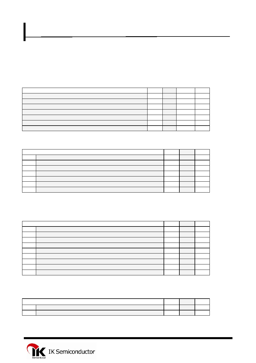
7. Operating Conditions
7.1. General Operating Conditions
MIN
NOM
MAX
UNIT
Supply Voltage, Vcc
4.75
5 5.25
V
Clock high-level input voltage at XTAL1, V
IH(CLK)
2
Vcc
V
Clock low-level input voltage at XTAL1, V
IL(CLK)
-0.5
0.8
V
High-level input voltage, V
IH
2.0
Vcc+0.5
V
Low-level input Voltage, V
IL
-0.5
0.8
V
Clock frequency, f
CLOCK
16
MHz
Operating free-air temperature, T
A
-40
80
o
C
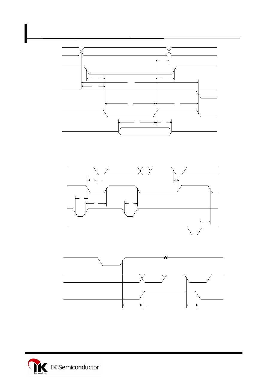
7.2. Read cycle timing requirements over recommended ranges of operating free-air temperature and supply
voltage (See Fig 1.)
MIN
MAX UNIT
t
rd
Pulse duration, IOR# low
75
ns
t
csr
Set up time, CSx# valid before IOR# low
10
ns
t
ar
Set up time, A2~A0 valid before IOR# low
15
ns
t
ra
Hold time, A2~A0 valid after IOR# high
0
ns
t
rcs
Hold time, CSx# valid after IOR# high
0
ns
t
frc
Delay time, t
ar
+t
rd
+t
rc
140
ns
t
rc
Delay time, IOR# high to IOR# or IOW# low
50
ns
The internal address strobe is always in active state.
In the FIFO mode, t
d1
=425ns (min) between reads of the FIFO and the status register.
7.3. Write cycle timing requirements over recommended ranges of operating free-air temperature and supply
voltage (See Fig 2.)
MIN
MAX UNIT
t
wr
Pulse duration, IOW# 50
ns
t
csw
Setup time, CSx# valid before IOW# 10
ns
t
aw
Setup time, A2~A0 valid before IOW# 15
ns
t
ds
Setup time, D7~D0 valid before IOW# 10
ns
t
wa
Hold time, A2~A0 valid after IOW# 5
ns
t
wcs
Hold time, CSx# valid after IOW# 5
ns
t
dh
Hold time, D7~D0 valid after IOW# 25
ns
t
fwc
Delay time, t
aw
+t
wr
+t
wc
120
ns
t
wc
Delay time, IOW# to IOW# or IOR# 55
ns
7.4. Read cycle switching characteristics over recommended ranges of operating free-air temperature and supply
voltage ( See Fig 1.)
MIN
MAX UNIT
t
rvd
Enable time, IOR# to D7~D0 valid
30 ns
t
hz
Disable time, IOR# to D7~D0 released
0
20 ns
5
15

IN16C554PL/IN16C554TQ
QUAD-UART
ASYNCHRONOUS COMMUNICATIONS ELEMENT
7.5. Transmitter switching characteristics over recommended ranges of operating free-air temperature and
supply voltage (See Fig 3~5.)
MIN
MAX UNIT
t
irs
Delay time, INTx to TXDx at start
8
24 RCLK
cycles
t
sti
Delay time, TXDx at start to INTx 8
8 RCLK
cycles
t
si
Delay time, IOW# high or low (WR THR) to INTx 16
32 RCLK
cycles
t
sxa
Delay time, TXDx at start to TXRDY#
8 RCLK
cycles
t
hr
Propagation delay time, IOW#(WR THR) to INTx
35 ns
t
ir
Propagation delay time, IOR#(RD IIR) to INTx
30 ns
t
wxi
Propagation delay time, IOW#(WR THR) to TXRDY#
50 ns
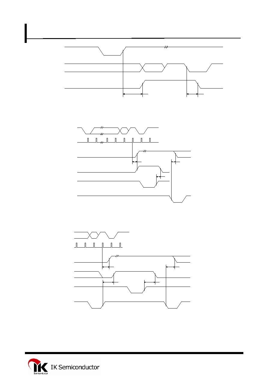
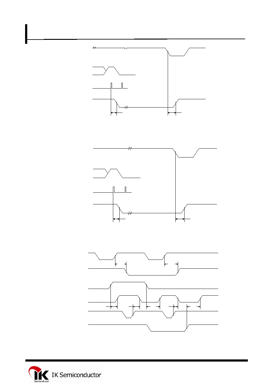
7.6. Receiver switching characteristics over recommended ranges of operating free-air temperature and supply
voltage (Fig 6~9.)
MIN
MAX UNIT
t
sint
Delay time, stop bit to INTx or stop bit to RXRDY# or read RBR to set interrupt
1 RCLK
cycle
t
rint
Propagation delay time, Read RBR/LSR to INTx/LSR interrupt
40 ns
t
rint
Propagation delay time, IOR# RCLK to RXRDY#
40 ns
7.7. Modem control switching characteristics over recommended ranges of operating free-air temperature and
supply voltage (See Fig 10.)
MIN
MAX
t
mdo
Propagation delay time, IOW#(WR MCR) to RTSx#, DTRx#
50 ns
t
sim
Propagation delay time, modem input CTSx#, DSRx#, and DCDx# to INTx
30 ns
t
rim
Propagation delay time, IOR#(RD MSR) to interrupt
35 ns
t
sim
Propagation delay time, Rix# to INTx#
30 ns
A[2:0]
hz
csr
t
ar
IOR#
t
t
t
t
t
t
t
tfrc
ACTIVE
D[7:0]
rcs
ra
VALID ADDRESS
CSx#
rd
rc
VALID DATA
rvd
IOW#
Fig 1. Read Cycle Timing
5
16
IN16C554PL/IN16C554TQ
QUAD-UART
ASYNCHRONOUS COMMUNICATIONS ELEMENT
fwc
wr
t
dh
ACTIVE
t
t
wa
t
t
D[7:0]
t
wc
t
A[2:0]
t
VALID DATA
t
VALID ADDRESS
CSx#
aw
wcs
csw
ds
IOW#
IOR#
Fig 2. Write Cycle Timing Waveforms
hr
t
irs
t
tsti
si
hr
TXDx
t
PARITY
t
INTx
ir
IOW#
START
IOR#
START
(WR THR)
(RD IIR)
STOP(1-2)
DATA(5-8)
t
Fig 3. Transmitter Timing Waveforms
IOW#
(WR THR)
tsxa
t
TXRDY#
STOP
wxi
PARITY
TXDx
START
DATA
BYTE #1
Fig 4. Transmitter Ready Mode 0 Timing Waveforms
5
17
IN16C554PL/IN16C554TQ
QUAD-UART
ASYNCHRONOUS COMMUNICATIONS ELEMENT
sxa
(WR THR)
TXRDY#
wxi
IOW#
STOP
BYTE #16
t
FIFO FULL
t
START
PARITY
DATA
TXDx
Fig 5. Transmitter Ready Mode 1 Timing Waveforms
(FIFO AT OR ABOVE
t
(RD LSR)
sint
rint
IOR#
(RD RBR)
LSI INTERRUPT
(FCR6, 7 = 0, 0)
DATA(5-8)
START
INTx(TRIGGER
IOR#
LEVEL INTERRUPT
Clock
Sample
rint
t
RXDx
t
TRIGGER LEVEL)
STOP
(FIFO BELOW
PARITY
TRIGGER LEVEL)
Fig 6. Receiver FIFO First Byte (Sets RDR) Waveforms
TRIGGER LEVEL
Clock
STOP
TRIGGER LEVEL)
sint
(RD LSR)
t
sint
t
IOR#
rint
(RD RBR)
t
rint
TRIGGER LEVEL)
t
RXDx
(FIFO AT OR ABOVE
Sample
INTERRUPT
TOP BYTE OF FIFO
(FIFO BELOW
READ FROM FIFO
LSI INTERRUPT
PREVIOUS BYTE
IOR#
TIMEOUT OR
Fig 7. Receiver FIFO After First Byte (After RDR Set) Waveforms
5
18
IN16C554PL/IN16C554TQ
QUAD-UART
ASYNCHRONOUS COMMUNICATIONS ELEMENT
RXDx
t
RXRDY#
rint
(RD RBR)
IOR#
Clock
Sample
sint
t
STOP
(FIRST BYTE)
Fig 8. Receiver Ready Mode 0 Timing Waveforms
Sample
sint
REACHES THE
RXDx
t
TRIGGER LEVEL)
t
IOR#
rint
RXRDY#
Clock
(FIRST BYTE THAT
STOP
(RD RBR)
Fig 9. Receiver Ready Mode 1 Timing Waveforms
sim
RTSx#, DTRx#
(WR MCR)
t
t
rim
t
t
sim
rim
t
sim
t
IOW#
mdo
(RD MSR)
mdo
IOR#
t
INTx
CTSx#, DSRx#, DCDx#
RIx#
Fig 10. Modem Control Timing Waveforms
5
19

IN16C554PL/IN16C554TQ
QUAD-UART
ASYNCHRONOUS COMMUNICATIONS ELEMENT
* Typical Clock Circuits
-
C1 : 10~30pF, C2 : 40~60pF, R1 : 1M, R2 : 1.5K
8. Mechanical Data
PLCC(Plastic Leaded Chip Carrier) Package
0.956 (24,282)
0.
956 (24,
282)
0.02 (0,51) MIN
0.18 (4,57) MAX
0.120 (3,05)
0.090 (2,29)
0.
469 (11,
913)
0.
469 (11,
913)
0.
021 (0,
53)
0.
013 (
0
,3
3)
0.
032 (0.0
81)
0.
050 (
1
,2
7)
0.026
(0,
66)
0.985 (25,019)
0.950 (24,130)
0.
985 (25,0
19)
0.
950 (
2
4,13
0)
0.4
41 (1
1,20
1)
0.
441 (11,
201)
0.
995 (25,
273)
0.995 (25,273)
Note
1.
All dimensions are in inches (millimeters).
2.
Falls within ANSI Y14.5-1982
IN16C554
XTAL1
XTAL2
C1
Crystal
R1
C2
R2
5
20

IN16C554PL/IN16C554TQ
QUAD-UART
ASYNCHRONOUS COMMUNICATIONS ELEMENT
TQFP(Thin Quad Flat Pack) Package
0 - 7
0,75
1.00
0,45
0,10
1,05
1,20
MAX
0,95
9,50
12,00
14,00
0,50
0,27
0,17
Note
1. All dimensions are in millimeters.
2. Falls within ANSI Y14.5-1982.
5
21