TECHNICAL DATA
1
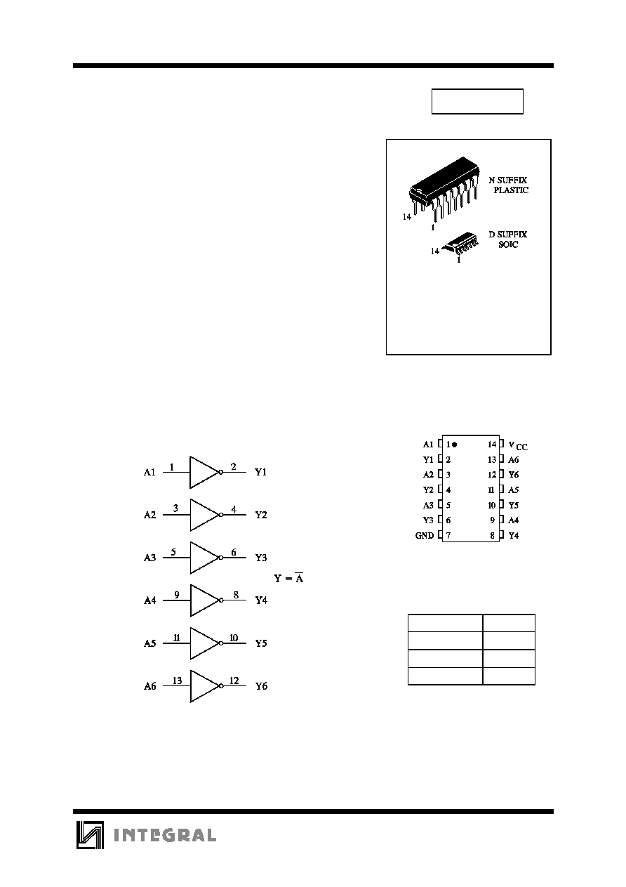
Hex Inverter
Advanced Low Power Schottky TTL
This device contains six independent gates, each of which performs
the logic INVERT function.
∑
Operating Voltage Range: 4.5 V to 5.5 V
∑
Guarantee DC and AC specification over full temperature and V
CC
range
∑
Switching response specified into 500
/50 pF
∑
Output Current:
IN74ALS04
ORDERING INFORMATION
IN74ALS04N Plastic
IN74ALS04D SOIC
T
A
= -10
∞
to 70
∞
C
for all packages
LOGIC DIAGRAM
PIN 14 =V
CC
PIN 7 = GND
PIN ASSIGNMENT
FUNCTION TABLE
Inputs
Output
A
Y
L
H
H
L
High Level: -0.4 mA
Low Level : 8 mA
IN74ALS04
2
MAXIMUM RATINGS
*
Symbol
Parameter
Value
Unit
V
CC
Supply Voltage
7.0
V
V
IN
Input Voltage
7.0
V
V
OUT
Output Voltage
5.5
V
Tstg
Storage Temperature Range
-65 to +150
∞
C
*
Maximum Ratings are those values beyond which damage to the device may occur.
Functional operation should be restricted to the Recommended Operating Conditions.
RECOMMENDED OPERATING CONDITIONS
Symbol
Parameter
Min
Max
Unit
V
CC
Supply Voltage
4.5
5.5
V
V
IH
High Level Input Voltage
2.0
V
V
IL
Low Level Input Voltage
0.8
V
I
OH
High Level Output Current
-0.4
mA
I
OL
Low Level Output Current
8.0
mA
T
A
Ambient Temperature Range
-10
+70
∞
C
DC ELECTRICAL CHARACTERISTICS over full operating conditions
Guaranteed Limit
Min
Max
V
IK
Input Clamp Voltage
V
CC
= min, I
IN
= -18 mA
-1.5
V
V
OH
High Level Output Voltage
V
CC
= min, I
OH
= -0.4 mA
2.5
V
V
OL
Low Level Output Voltage
V
CC
= min, I
OL
= 4 mA
0.4
V
V
CC
= min, I
OL
= 8 mA
0.5
I
IH
High Level Input Current
V
CC
= max, V
IN
= 2.7 V
20
µ
A
V
CC
= max, V
IN
= 7.0 V
0.1
mA
I
IL
Low Level Input Current
V
CC
= max, V
IN
= 0.4 V
-0.1
mA
I
OS
Output Short Circuit Current
V
CC
= max, V
O
= 2.25 V
-15
-70
mA
I
CC
Supply Current
V
CC
= max
Outputs High
1.1
mA
Outputs Low
4.2
Parameter
Test Conditions
Symbol
Unit
IN74ALS04
3
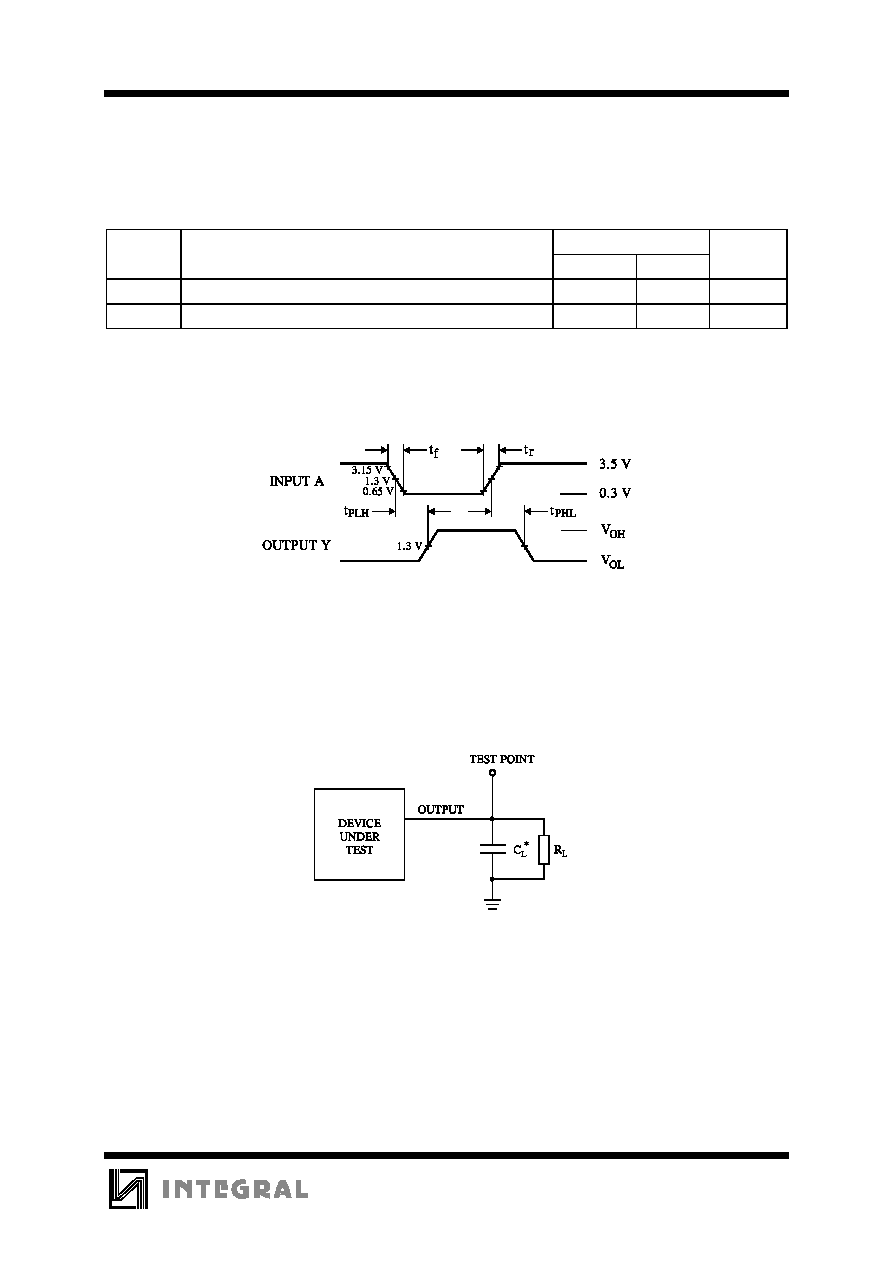
AC ELECTRICAL CHARACTERISTICS over full operating conditions
(V
CC
= 5.0 V
±
10%,
C
L
= 50 pF, R
L
= 500
, Input t
r
= t
f
= 2.0 ns)
Guaranteed Limit
Min
Max
t
PLH
Propagation Delay, Input A to Output Y (Figures 1,2)
11
ns
t
PHL
Propagation Delay, Input A to Output Y (Figures 1,2)
8
ns
Figure 1. Switching Waveforms
* Includes all probe and jig capacitance
Figure 2. Test Circuit
Parameter
Symbol
Unit