
TECHNICAL DATA
1
OCTAL BUS TRANSCEIVER (3-State)
By pinning IN74LV245 are compatible with IN74HC245A and
IN74HCT245A series. Input voltage levels are compatible with
standard CMOS levels.
∑ Output voltage levels are compatible with input levels of
CMOS, NMOS and TTL IC
S
∑ Supply voltage range: 2.0 to 3.2 V
∑ Low input current: 1.0 µ; 0.1 µ at = 25 ∞
∑ Output current 8 m
∑ Latch current value: not less 150 m at = 125 ∞
∑ ESD acceptable values: not less than 2000 V as per HBM
and not less 200 V as per
∑
IN74LV245
N SUFFIX
PLASTIC
D SUFFIX
SOIC
1
20
1
20
ORDERING INFORMATION
IN74LV245N Plastic DIP
IN74LV245D SOIC
T
A
= -40
∞ to 125∞ C
for all packages
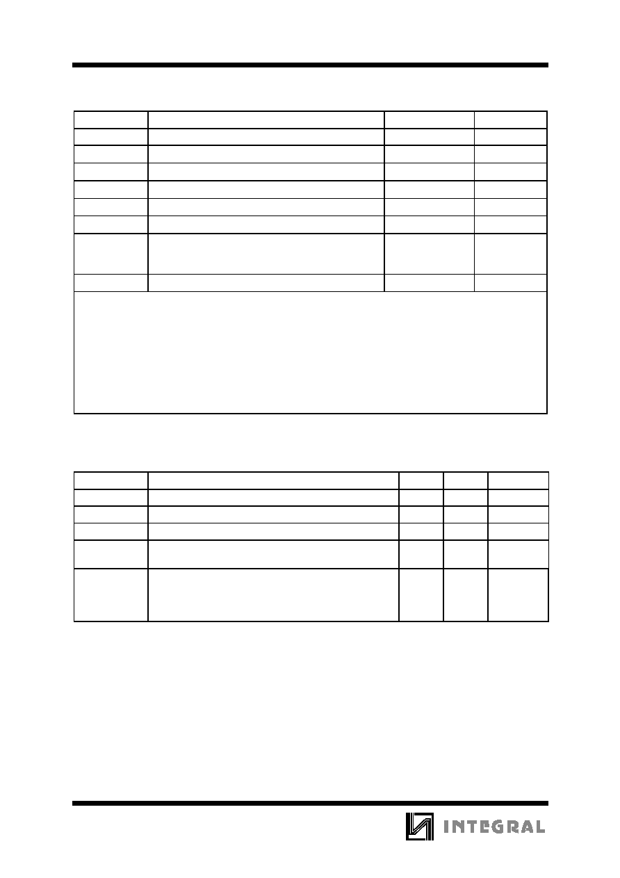
PIN ASSIGNMENT
245
DIR
01
A
0
02
A
1
03
A
2
04
A
3
05
A
4
06
A
5
07
A
6
08
A
7
09
GND
10
20
19
18
17
16
15
14
13
12
11
B
0
B
1
B
2
B
3
B
4
B
5
B
6
B
7
OE
V
CC
FUNCTION TABLE
Inputs
Inputs/Outputs
OE
DIR
L
L
A=B
input
L
H
input
B=A
H
X
Z
Z
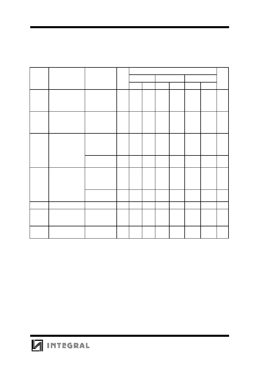
BLOCK DIAGRAM
18
B
0
03
17
B
1
A
1
04
16
B
2
A
2
05
15
B
3
A
3
06
14
B
4
A
4
07
13
B
5
A
5
08
12
B
6
A
6
09
11
B
7
A
7
01
DIR
02
A
0
19
OE
Pin 20=V
CC
Pin 10 = GND
IN74LV245
2
ABSOLUTE MAXIMUM RATINGS*
Symbol
Parameter
Rating
Unit
V
CC
Supply voltage
-0.5 to +5.0
V
I
IK
*
1
Input diode current
±20
m
I
OK
*
2
Output diode current
±50
m
I
O
*
3
Output source or sink current
±35
m
I
CC
V
CC
current
±70
m
I
GND
GND current
±70
m
P
D
Power dissipation per package:
Plastic DIP *
4
SOIC *
4
750
500
mW
Tstg
Storage temperature range
-65 to +150
∞C
*
In absolute maximum ratings modes functioning is not guaranteed. Vpon lifting the absolute
maximum ratings functioning is guaranteed at the recommended operating conditions.
*
1
Provided V
I
< -0.5 V or V
I
> V
CC
+ 0.5 V.
*
2
Provided V
O
< -0.5 V or V
O
> V
CC
+ 0.5 V.
*
3
Provided -0.5 V < V
O
< V
CC
+ 0.5 V.
*
4
When operating in the temperature range of 70
∞ to 125∞C power dissipation value decreases:
- for Plastic DIP by 12 mW/
∞C
- for SOIC by 8 mW/
∞C
RECOMMENDED OPERATING CONDITIONS
Symbol
Parameter
Min
Max
Unit
V
CC
Supply voltage
1.2
3.6
V
V
IN
Input voltage
0
V
CC
V
V
OUT
Output voltage
0
V
CC
V
T
A
Operating ambient temperature range. For all
package types
-40
125
∞C
t
LH
, t
HL
Input rise and fall times
V
CC
=1.2 V
V
CC
=2.0 V
V
CC
=3.0 V
V
CC
=3.6 V
0
1000
700
500
400
ns
IN74LV245
3
DC CHARACTERISTICS
Test
V
CC
,
Limits
Symbol
Parameter
conditions
V
25
∞
∞
∞
∞C
-40
∞
∞
∞
∞C to 85∞∞∞∞C
125
∞
∞
∞
∞C
Unit
min max
min
max
min
max
V
IH
HIGH level input
voltage
V
O
= V
CC
-0.1 V
1.2
2.0
3.0
3.6
0.9
1.4
2.1
2.5
-
-
-
-
0.9
1.4
2.1
2.5
-
-
-
-
0.9
1.4
2.1
2.5
-
-
-
-
V
V
IL
LOW level output
voltage
V
O
=0.1 V
1.2
2.0
3.0
3.6
-
-
-
-
0.3
0.6
0.9
1.1
-
-
-
-
0.3
0.6
0.9
1.1
-
-
-
-
0.3
0.6
0.9
1.1
V
V
OH
HIGH level
output voltage
V
I
= V
IH
or V
IL
I
O
= -50
µ
1.2
2.0
3.0
3.6
1.1
1.92
2.92
3.52
-
-
-
-
1.0
1.9
2.9
3.5
-
-
-
-
1.0
1.9
2.9
3.5
-
-
-
-
V
V
I
= V
IH
or V
IL
I
O
= -8 m
3.0
2.48
-
2.34
-
2.20
-
V
V
OL
LOW level output
voltage
V
I
= V
IH
or V
IL
I
O
= 50
µ
1.2
2.0
3.0
3.6
-
-
-
-
0.09
0.09
0.09
0.09
-
-
-
-
0.1
0.1
0.1
0.09
-
-
-
-
0.1
0.1
0.1
0.09
V
V
I
= V
IH
or V
IL
I
O
= 8 m
3.0
-
0.33
-
0.4
-
0.5
V
I
I
Input current
V
I
= V
CC
or 0 V
3.6
-
±0.1
-
±1.0
-
±1.0
µ
I
OZ
OFF-state
current
3-state outputs
V
I
= V
IL
or V
IH
V
O
=V
CC
or 0 V
3.6
-
±0.5
-
±5
-
±10
µ
I
CC
Supply current
V
I
=V
CC
or 0 V
I
O
= 0
µ
3.6
-
8.0
-
80
-
160
µ

IN74LV245
4
AC CHARACTERISTICS
(C
L
=50 pF, t
LH
= t
HL
= 6.0 ns)
Test
V
CC
,
Limits
Symbol
Parameter
conditions
V
25
∞
∞
∞
∞C
-40
∞
∞
∞
∞C to
85
∞
∞
∞
∞C
125
∞
∞
∞
∞C
Unit
min max min
max
min
max
t
PHL,
t
PLH
from An to Bn,
from Bn to An
Propagation
delay
Figure 1
1.2
2.0
3.0
-
-
-
100
23
14
-
-
-
125
28
18
-
-
-
140
34
21
ns
t
PHZ
t
PLZ
from OE, DIR
to An, Bn
3-state output
enable time
Figure 2
1.2
2.0
3.0
-
-
-
120
30
20
-
-
-
140
37
24
-
-
-
160
43
28
ns
t
PZH
t
PZL
from OE to
An, Bn
3-state output
disable time
Figure 2
1.2
2.0
3.0
-
-
-
120
28
17
-
-
-
140
35
21
-
-
-
160
43
26
t
THL,
t
TLH
HIGH-to-LOW
and LOW-to
HIGH transition
time
Figure 1
1.2
2.0
3.0
-
-
-
60
15
10
-
-
-
75
20
13
-
-
-
90
24
15
C
I
Input
capacitance
For inputs
01,19
3.0
-
7
-
-
-
-
pF
C
I/
Input
capacitance
For inputs/
outputs
02-09,
11-18
3.0
-
20
-
-
-
-
C
PD
Power
dissipation
capacitance
(per one
channel)
V
I
= 0 V or
V
CC
3.0
-
50
-
-
-
-

IN74LV245
5
0.9
V
1
0.1
0.9
V
1
0.1
0.9
V
1
0.1
0.9
V
1
0.1
t
LH
t
HL
t
PHL
t
PLH
t
TLH
t
THL
V
CC
GND
An, Bn
V
1
= 0.5V
CC
Bn, An
0 B
Figure 1 -Time diagram of AC parameters control t
PLH
, t
PHL.
0.9
V
1
0.1
0.9
V
1
0.1
t
LH
t
HL
V
CC
GND
OE, DIR
V
1
0.9
0.1
V
1
t
PZH
t
PZL
t
PHZ
t
PLZ
An, Bn
An, Bn
V
OH
0 B
V
CC
V
OL
V
1
= 0.5V
CC
Figure 2 - Time diagram of t
PLZ
, t
PHZ
, t
PZL
, t
PZH.
AC parameters control
V
V
IN74LV245
6
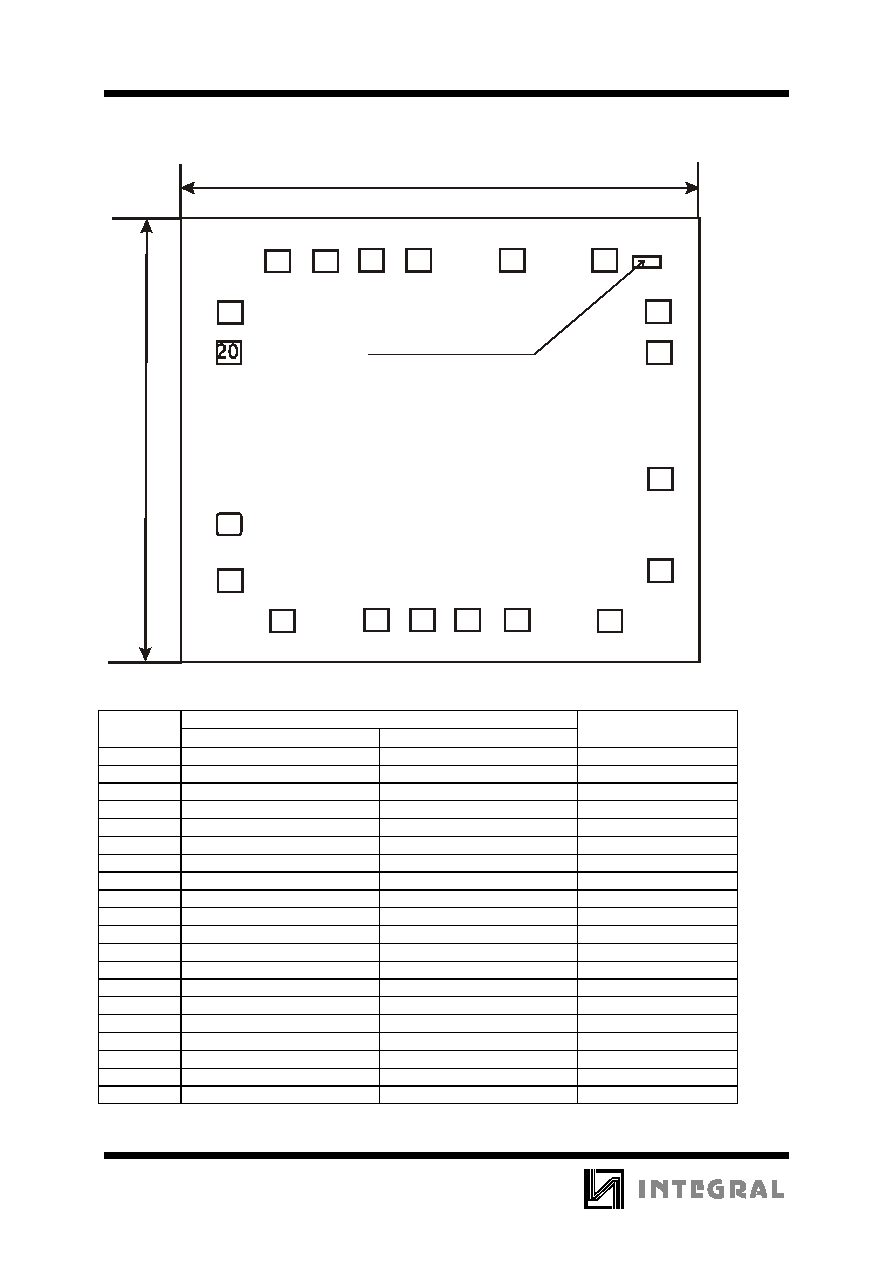
Drawing of the chip
Pads allocation Table
coordinates (counted from lower left corner), mm
Pad
number
X
Y
Pad size, mm
01
0.140
0.573
0.108 x 0.108
02
0.140
0.315
0.108 x 0.108
03
0.370
0.140
0.108 x 0.108
04
0.790
0.140
0.108 x 0.108
05
1.000
0.140
0.108 x 0.108
06
1.200
0.140
0.108 x 0.108
07
1.417
0.140
0.108 x 0.108
08
1.833
0.140
0.108 x 0.108
09
2.060
0.354
0.108 x 0.108
10
2.060
0.760
0.108 x 0.108
11
2.060
1.340
0.108 x 0.108
12
2.060
1.520
0.108 x 0.108
13
1.833
1.750
0.108 x 0.108
14
1.415
1.750
0.108 x 0.108
15
1.000
1.750
0.108 x 0.108
16
0.790
1.750
0.108 x 0.108
17
0.580
1.750
0.108 x 0.108
18
0.370
1.750
0.108 x 0.108
19
0.140
1.544
0.108 x 0.108
20
0.140
1.375
0.108 x 0.108
1
2
3
4
5
6
7
8
9
10
11
12
13
14
15
16
17
18
19
2.3mm
1
.99 m
m
74LV245
On-chip marking