TECHNICAL DATA
IN74LV373
OCTAL D-TYPE TRANSPARENT LATCH (3-State)
IN74LV373 are compatible by pinning with IN74HC373A and
IN74HCT373A series. Input voltage levels are compatible with
standard CMOS levels.
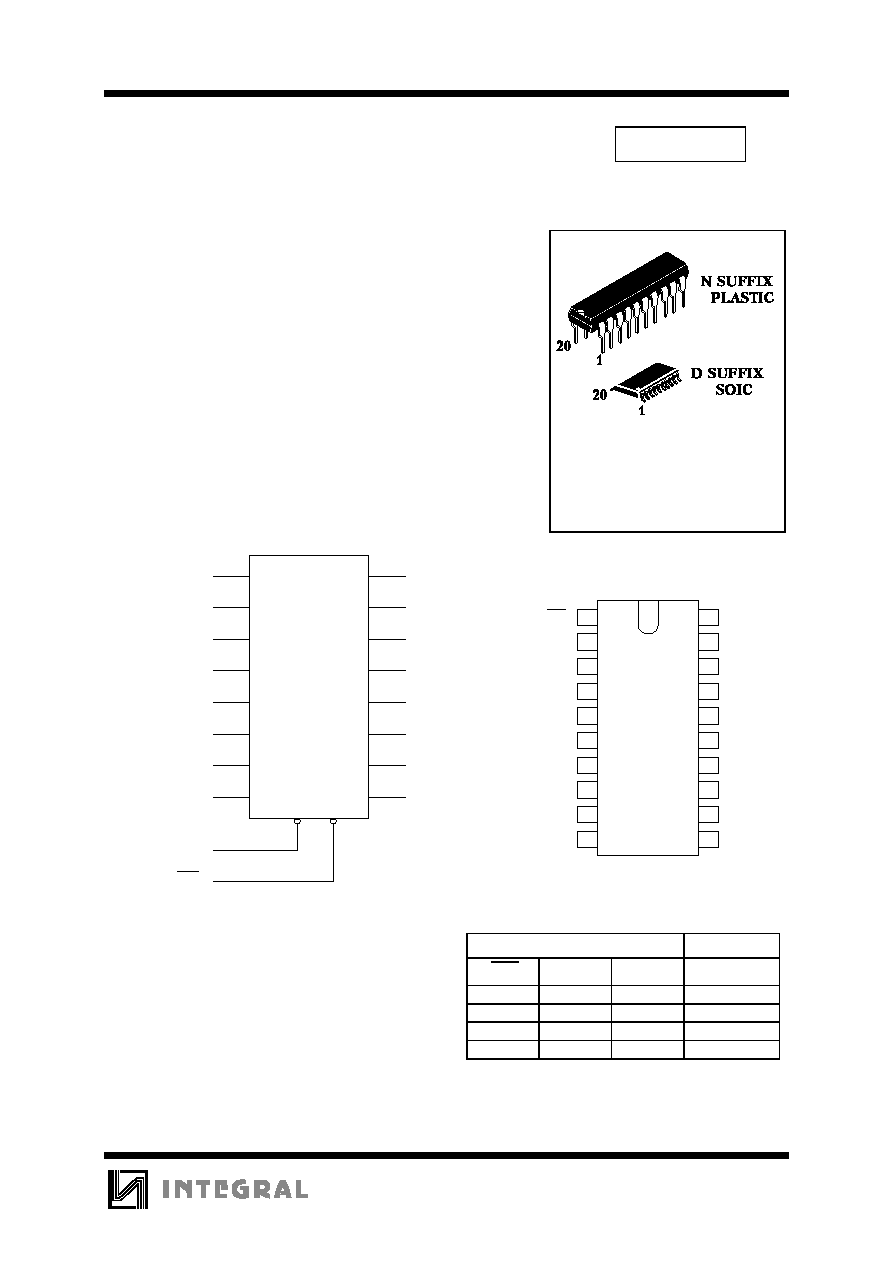
ORDERING INFORMATION
IN74LV373N Plastic DIP
IN74LV373D SOIC
T
A
= -40
∞ to 125∞ C
for all packages
∑ Output voltage levels are compatible with input levels of
CMOS, NMOS and TTL IC
S
∑ Voltage supply range: 2.0 to 3.2 V
∑ LOW input current: 1.0 µ; 0.1 µ at = 25 ∞
∑ Input current LOW/HIGH: 8 m
∑ Latch current: not less than 150 m at = 125 ∞
∑ ESD acceptable value: not less than 2000 V as per HBM
and not less than 200 V as per MM
∑
BLOCK DIAGRAM
OE
01
Q
0
02
D
0
03
D
1
04
Q
1
05
Q
2
06
D
2
07
D
3
08
Q
3
09
19
18
17
16
15
14
13
12
11
D
7
D
6
Q
6
Q
5
D
5
D
4
Q
4
LE
Q
7
Pin 20=V
CC
Pin 10 = GND
PIN ASSIGNMENT
373
OE
01
Q
0
02
D
0
03
D
1
04
Q
1
05
Q
2
06
D
2
07
D
3
08
Q
3
09
GND
10
20
19
18
17
16
15
14
13
12
11
D
7
D
6
Q
6
Q
5
D
5
D
4
Q
4
LE
V
CC
Q
7
FUNCTION TABLE
Inputs Output
OE LE Dn Qn
L H H H
L H L L
L L X
no
change
H X X Z
1

IN74LV373
ABSOLUTE MAXIMUM RATINGS*
Symbol Parameter Rating
Unit
V
CC
Supply voltage
-0.5 to +5.0
V
I
IK
*
1
Input diode current
±20
m
I
OK
*
2
Output diode current
±50
m
I
O
*
3
Output source or sink current
±35
m
I
CC
V
CC
current
±70
m
I
GND
GND
current
±70
m
P
D
Power dissipation per package:
Plastic DIP *
4
SOIC *
4
750
500
mW
Tstg
Storage temperature range
-65 to +150
∞C
*
In absolute maximum ratings modes functioning is not guaranteed. Upon lifting the absolute
maximum ratings functioning is guarateed at the recommended operatng conditions.
*
1
Provided V
I
< -0.5 V or V
I
> V
CC
+ 0.5 V.
*
2
Provided V
O
< -0.5 V or V
O
> V
CC
+ 0.5 V.
*
3
Provided -0.5 V < V
O
< V
CC
+ 0.5 V.
*
4
When operating in the temperature range of 70
∞ to 125∞C power dissipation value decreses:
- for Plastic DIP by 12 mW/
∞C
- for SOIC by 8 mW/
∞C
RECOMMENDED OPERAING CONDITIONS
Symbol Parameter Min
Max
Unit
V
CC
Supply
voltage
1.2 3.6 V
V
IN
Input
voltage
0 V
CC
V
V
OUT
Output
voltage
0 V
CC
V
T
A
Operating ambient temperature range.
For all types of packages
-40 125
∞C
t
LH
, t
HL
Input rise and fall times
V
CC
=1.2 V
V
CC
=2.0 V
V
CC
=3.0 V
V
CC
=3.6 V
0 1000
700
500
400
ns
2
IN74LV373
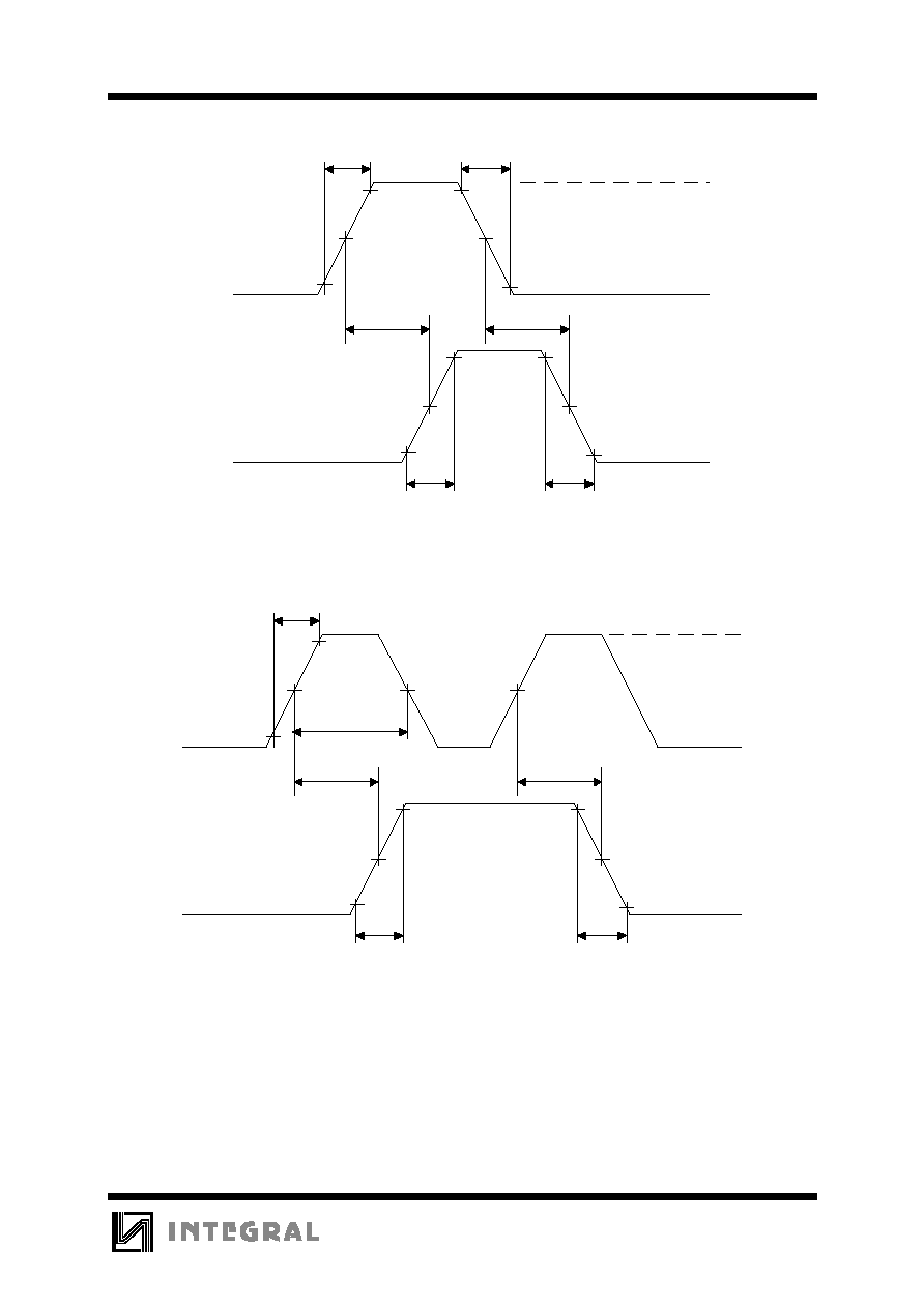
AC CHARACTERISTICS
(C
L
=50 pF, t
LH
= t
HL
= 6.0 ns)
Test
V
CC
, Limits
Symbol Parameter
conditions
V
25
∞C
-40
∞C to
85
∞C
125
∞C
Unit
min
max
min
max
min
max
t
PHL,
t
PLH
from Dn to Qn
Propagation delay Figure 1
1.2
2.0
3.0
-
-
-
150
38
23
-
-
-
190
48
29
-
-
-
220
58
35
ns
t
PHL,
t
PLH
from LE to Qn
Propagation delay Figure 2
1.2
2.0
3.0
-
-
-
180
45
27
-
-
-
230
56
34
-
-
-
270
68
41
t
PHZ
t
PLZ
from OE to
Qn
3-state output
enable time
Figure 4
1.2
2.0
3.0
-
-
-
160
35
23
-
-
-
200
43
28
-
-
-
240
45
32
t
PZH
t
PZL
from OE to
Qn
3-state disable
time
Figure 4
1.2
2.0
3.0
-
-
-
160
40
24
-
-
-
200
50
30
-
-
-
240
60
36
t
THL,
t
TLH
HIGH-to-LOW
and LOW-to-
HIGH transition
time
Figures 1,2
1.2
2.0
3.0
-
-
-
75
16
10
-
-
-
100
20
13
-
-
-
120
24
15
t
W
Clock pulse width
HIGH or LOW
Figure 2
1.2
2.0
3.0
250
30
18
-
-
-
350
34
20
-
-
-
450
41
24
-
-
-
t
SU
Set-up time Dn to
LE
Figure 3
1.2
2.0
3.0
45
15
9
-
-
-
50
17
10
-
-
-
100
15
12
-
-
-
t
H
Hold time Dn to
LE
Figure 3
1.2
2.0
3.0
25
5
5
-
-
-
25
5
5
-
-
-
25
5
5
-
-
-
C
I
Input
capacitance
3.0
- 7 - - - - pF
C
PD
Power
dissipation
capacitance (per
flip-flop)
V
I
= 0 V or
V
CC
3.0
-
80
- - - -
4