 | –≠–ª–µ–∫—Ç—Ä–æ–Ω–Ω—ã–π –∫–æ–º–ø–æ–Ω–µ–Ω—Ç: IN75232N | –°–∫–∞—á–∞—Ç—å:  PDF PDF  ZIP ZIP |
TECHNICAL DATA
Description
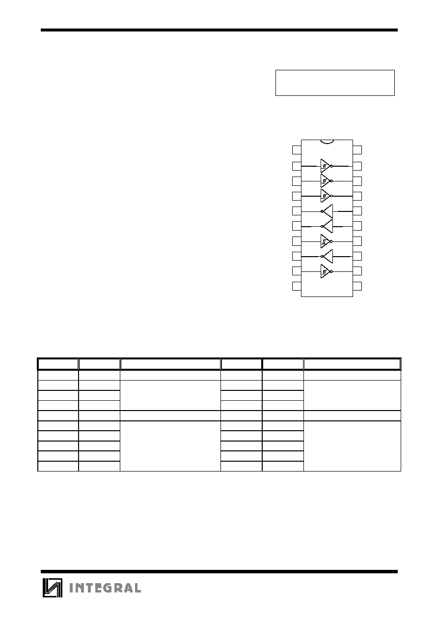
The IL75232N, IL75232ND are monolithic device
containing 3 independent drives and 5 receivers. These are
designed to interface between date terminal equipment and
date communication equipment as designed by EIA-232-D.
Features
∑ Meets standard EIA-232-D (Revision of RS-232-C)
∑ Drivers
- Current Limited Output 10 mA Typical
- Power-off Output Impedance 300
Min
- Slew Rate Control by Load Capacitor
- Flexible Supply Voltage Range
- Input Compatible with Most TTL and DTL Circuits
∑ Receivers
- Input Resistance 3 k
to 7 k
- Input Signal Range
± 30 V
- Built-in Input Hysteresis (Double Threshold)
∑ 20 DIP/SO20: S-001AD (IL75232N) / S-013A
(IL75232D)
Pin Description
Name
Pin No
Function
Name
Pin No
Function
V
CC+
1
Driver Section Supply +
V
CC-
10
Driver Section Supply -
DA1
16
DY1
5
DA2
15
DY2
6
Driver Output
DA3
13
Driver Input
DY3
8
V
CC
20
Receiver Section Supply
GND
11
Ground
RA1
2
RY1
19
RA2
3
RY2
18
RA3
4
Receiver Input
RY3
17
Receiver Output
RA4
7
RY4
14
RA5
9
RY5
12
Absolute Maximum Ratings
V
C C -
R A 5
D Y 3
R A 4
D Y 2
D Y 1
R A 3
R A 2
R A 1
V
C C +
10
9
8
7
6
5
4
3
2
1
11
12
13
14
15
16
17
18
19
20
G N D
R Y 5
D A 3
R Y 4
D A 2
D A 1
R Y 3
R Y 2
R Y 1
V
C C
B lock D iagram
IL 75232N , IL 75232D
IL75232N, IL75232D
EIA-232-D INTERFACE 1 CHIP IC
IL75232
Symbol
Parameter
Rating
Unit
V
CC+
Supply Voltage
15
V
V
CC-
Supply Voltage
-15
V
V
CC
Supply Voltage
10
V
VI (Driver)
Input Voltage
-15
˜ +7
V
VI (Reciver)
Input Voltage
± 30
V
VO (Driver)
Output Voltage
-15
˜ +15
V
PT
Continuous Power Dissipation (Below 25
o
C)
1.0
W
T
STG
Storage Temperature
-65
˜ +175
o
C
Top
Operating Temperature
0
˜ +75
o
C
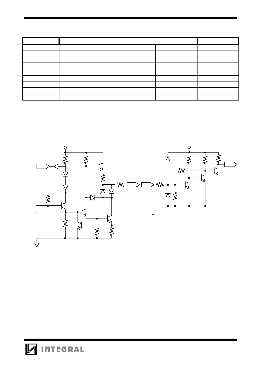
Schematic
V
CC-
300
70
6.2
8.2
70
7
10
3.6
V
CC+
DA
DY
DRIVER
RESEIVER
10
2
4
2
5
9
V
CC
DA
DY
TECHNICAL DATA
Electrical Characteristics
Supply Current
V
CC
= 5V, T
A
= 25
O
C
Symbol
Parameter
Test Conditions
Min
Max
Unit
I
CC+
Supply Current
V
CC+
= 9 V
V
IN
= 1.9V
15
mA
from V
CC+
No Load
V
IN
= 0.8V
4.5
V
CC+
= 12 V
V
IN
= 1.9V
19
No Load
V
IN
= 0.8V
5.5
V
CC+
= 15 V
V
IN
= 1.9V
25
No Load
V
IN
= 0.8V
9
I
CC-
Supply Current
V
CC-
= -9 V
V
IN
= 1.9V
-15
mA
from V
CC-
No Load
V
IN
= 0.8V
-3.2
V
CC-
= -12 V
V
IN
= 1.9V
-19
No Load
V
IN
= 0.8V
-3.2
V
CC-
= -15 V
V
IN
= 1.9V
-25
No Load
V
IN
= 0.8V
-3.2
I
CC
Supply Current
V
CC
= 5 V
V
IN
= 5.0V
30
mA
from V
CC
Driver Section
Symbol
Parameter
Test Conditions
Min
Max
Unit
V
IH
High Level
V
CC+
= 9 V
1.9
V
Input Voltage
V
CC-
= -9 V
V
IL
Low Level
0.8
V
Input Voltage
V
OH
High Level
V
IL
= 0.8V
V
CC+
= 9 V
6
V
Output Voltage
RL = 3 k
V
CC-
= -9 V
V
CC+
= 13.2 V
9
V
CC-
= -13.2 V
V
OL
Low Level
V
IH
= 1.9V
V
CC+
= 9 V
-6
V
Output Voltage
RL = 3 k
V
CC-
= -9 V
V
CC+
= 13.2 V
-9
V
CC-
= -13.2 V
I
IH
High Level
V
I
= 5V
10
µA
Input Current
I
IL
Low Level
V
I
= 0
-1.6
mA
Input Current
I
OS(H)
Short Circuit
V
I
= 0.8V
-6
-12
mA
Output Current
V
O
= 0
at High Level
I
OS(L)
Short Circuit
V
I
= 1.9V
6
12
mA
Output Current
V
O
= 0
at Low Level
R
O
Output Resistance,
V
CC+
= 0, V
CC-
= 0
300
Power Off
V
O
= -2V to 2V
IL75232
Driver Switching Characteristic
V
CC+
= 9V, V
CC-
= -9V T
A
= 25
O
C
Symbol
Parameter
Test Conditions
Min
Max
Unit
t
PLH
Propagation Delay Time,
RL = 3 k
500
ns
Low-To-High-Level Output
CL = 15
µF
t
PHL
Propagation Delay Time,
175
ns
High -To- Low -Level Output
See Figure 1
t
TLH
Transition Time,
100
ns
Low-To-High-Level Output *
t
THL
Transition Time,
75
ns
High -To- Low -Level Output*
t
TLH
Transition Time,
RL = 3 k
to 7 k
2.5
µs
Low-To-High-Level Output**
CL = 2500
F
(tip)
t
THL
Transition Time,
3.0
µs
High-To-Low -Level Output**
See Figure 1
(tip)
*- Measured between 10 % and 90 % Points of Output Waveform
** -
Measured between +3V and -3V Points on the Output Waveform (EIA-232-D Condition)
Receiver Section
Symbol
Parameter
Test Conditions
Min
Max
Unit
VT+
Positive-Going
1.75
2.25
V
Threshold Voltage
VT-
Negative-Going
0.75
1.25
V
Threshold Voltage
V
OH
High Level Output
V
I
= 0.75V, I
OL
=-0.5mA
2.6
5
V
Voltage
Input Open,
2.6
5
I
OL
= -0.5 mA
V
OL
Low Level Output Voltage
V
I
= 3V, I
OL
= 10 mA
0.45
V
I
IH
High-Level Input Current
V
I
= 25V
3.6
8.3
mA
V
I
= 3V
0.43
I
IL
Low-Level Input Current
V
I
= -25V
-3.6
-8.3
mA
V
I
= -3V
-0.43
I
OS
Short-Circuit
-3
mA
Output Current
(tip)
Receiver Switching Characteristic
V
CC
= 5V
Symbol
Parameter
Test Conditions
Min
Max
Unit
t
PLH
Propagation Delay Time,
C
L
= 15
F
150
ns
Low-To-High-Level Output
R
L
= 3.9 k
t
PHL
Propagation Delay Time,
C
L
= 15
F
50
ns
High -To- Low -Level Output
R
L
= 390 k
t
TLH
Transition Time,
C
L
= 15
F
175
ns
Low-To-High-Level Output
R
L
= 3.9 k
t
THL
Transition Time,
C
L
= 15
F
20
ns
High -To- Low -Level Output
R
L
= 390 k
TECHNICAL DATA
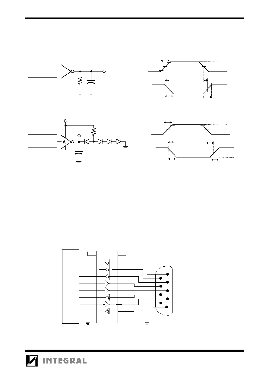
Parameter Measurement Information
DRIVER
C
L
R
L
Test Circuit
OUTPUT
PULSE
GENERATOR
(See Note A)
RESEIVER
V
CC
C
L
R1
Test Circuit
OUTPUT
(See Note C)
PULSE
GENERATOR
(See Note A)
Voltage Waveform
INTPUT
50%
50%
1.5V
1.5V
3V
V
OL
V
OH
OV
10ns
t
PHL
t
PLH
t
TLH
t
THL
OUTPUT
T
W
=25 µs, Voltage Waveform
INTPUT
1.5V
1.5V
50%
10%
10%
90%
90%
50%
3V
V
OL
V
OH
OV
10ns
t
PHL
t
PLH
t
TLH
t
THL
OUTPUT
Note
A.
The pulse generator has the following characteristics. f = 200 KHz, Z
O
= 50
B.
C included probe and jig capacitance.
C.
All diodes are 1N3064 or equivalent.
Fig1. Propagation and Transition Times
Typical Application
D B 95
SIO C ard
IL A 75232N ,D
9
8
6
7
5
4
3
2
1
+5V
T X
C T S
D TR
R I
-12V
/ R I
/ D T R
SO U T
/ C TS
R X
R T S
/ R TS
SIN
D SR
D C D
+12V
/ D C D
/ D SR
U A R T
IL75232
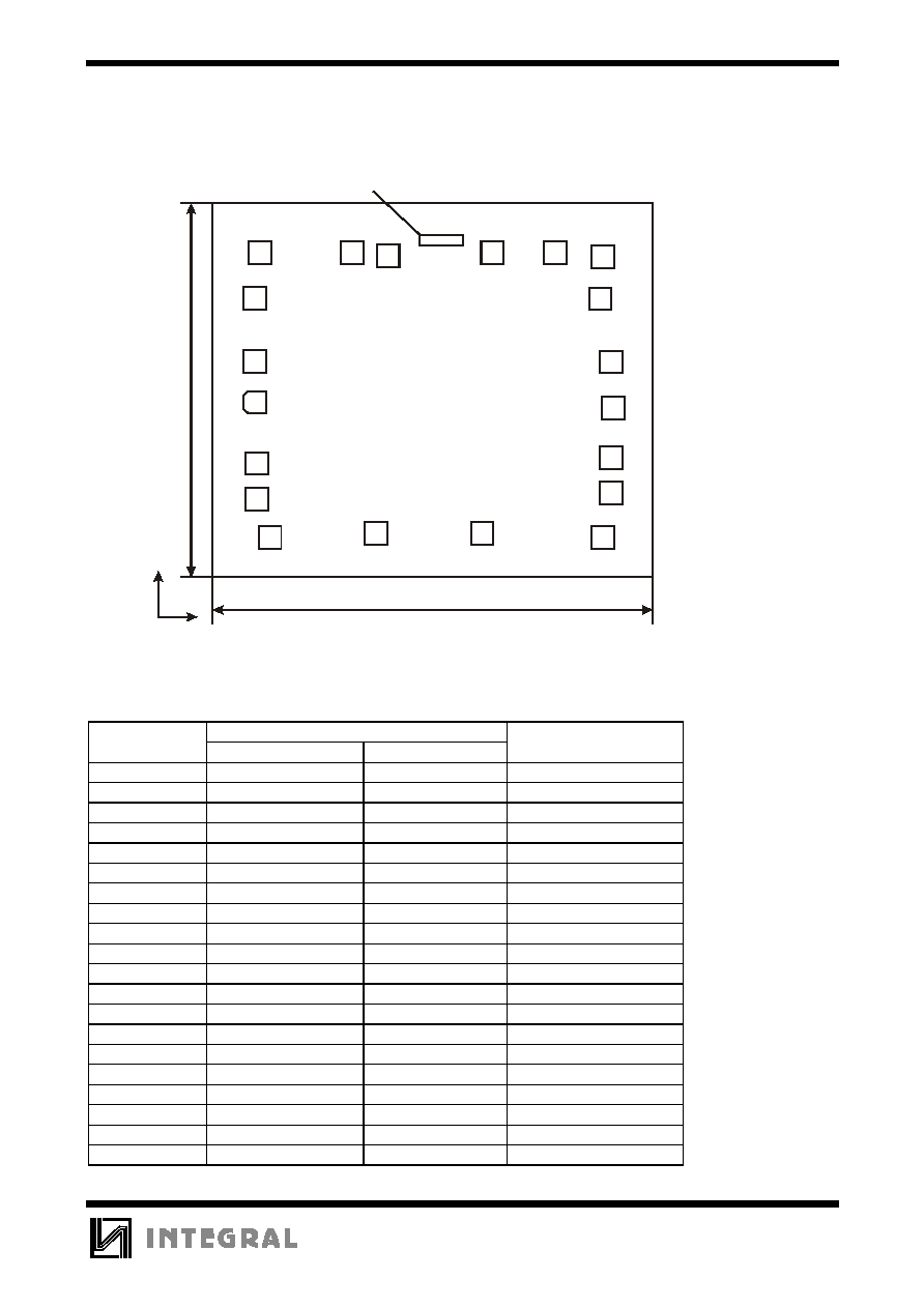
CHIP PAD DIAGRAM
Location of marking (mm): left lower corner x=0.942, y=1.506, right higher corner x=1.137, y=1.556.
PAD LOCATION
Location (left lower corner), mm
Pad No
X
Y
Pad size, mm
01
0.141
0.743
0.102 x 0.102
02
0.151
0.466
0.102 x 0.102
03
0.151
0.306
0.102 x 0.102
04
0.210
0.128
0.102 x 0.102
05
0.692
0.149
0.102 x 0.102
06
1.174
0.149
0.102 x 0.102
07
1.722
0.130
0.102 x 0.102
08
1.760
0.333
0.102 x 0.102
09
1.760
0.493
0.102 x 0.102
10
1.768
0.718
0.102 x 0.102
11
1.760
0.928
0.102 x 0.102
12
1.711
1.214
0.102 x 0.102
13
1.722
1.406
0.102 x 0.102
14
1.504
1.424
0.102 x 0.102
15
1.220
1.424
0.102 x 0.102
16
0.747
1.410
0.102 x 0.102
17
0.584
1.424
0.102 x 0.102
18
0.165
1.424
0.102 x 0.102
19
0.141
1.217
0.102 x 0.102
20
0.106
0.929
0.102 x 0.102
Note: Size is given as per passivation layer
01
19
15
20
16
02
03
04
05
06
07
08
09
10
11
12
17
13
18
14
2.0
1.7
Chip marking
75232
(0,0)
X
Y