 | –≠–ª–µ–∫—Ç—Ä–æ–Ω–Ω—ã–π –∫–æ–º–ø–æ–Ω–µ–Ω—Ç: IW4017BN | –°–∫–∞—á–∞—Ç—å:  PDF PDF  ZIP ZIP |
TECHNICAL DATA
29
Counter/Divider
High-Voltage Silicon-Gate CMOS
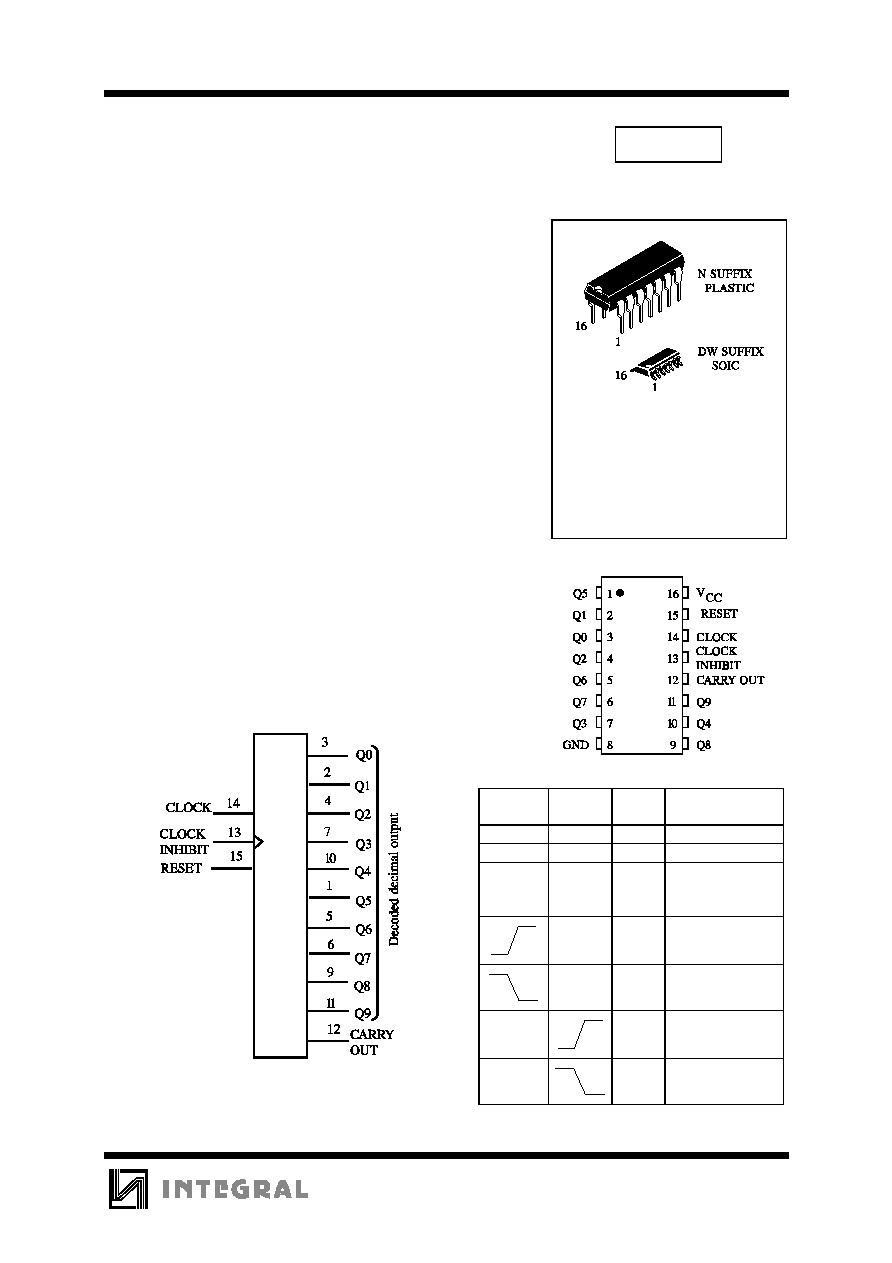
The IW4017B is 5-stage Johnson counter having 10 decoded
outputs. Inputs include a CLOCK, a RESET, and a CLOCK INHIBIT
signal. Schmitt trigger action in the CLOCK input circuit provides
pulse shaping that allows unlimited clock input pulse rise and fall
times.
The counter is advanced one count at the positive clock signal
transition if the CLOCK INHIBIT signal is low. Counter advancement
via the clock line is inhibited when the CLOCK INHIBIT signal is
high. A high RESET signal clears the counter to its zero count. Use of
the Johnson counter configuration permits high-speed operation, 2-
input decode-gating and spike-free decoded outputs. Anti-lock gating
is provided, thus assuring proper counting sequence. The decoded
outputs are normally low and go high only at their respective decoded
time slot. Each decoded output remains high for one full clock cycle. A
CARRY-OUT signal completes one cycle every 10 clock input cycles
in the IW4017B.
∑
Operating Voltage Range: 3.0 to 18 V
∑
Maximum input current of 1
µ
A at 18 V over full package-
temperature range; 100 nA at 18 V and 25
∞
C
∑
Noise margin (over full package temperature range):
1.0 V min @ 5.0 V supply
2.0 V min @ 10.0 V supply
2.5 V min @ 15.0 V supply
IW4017B
ORDERING INFORMATION
IW4017BN Plastic
IW4017BDW SOIC
T
A
= -55
∞
to 125
∞
C for all packages
PIN ASSIGNMENT
LOGIC DIAGRAM
PIN 16 =V
CC
PIN 8 = GND
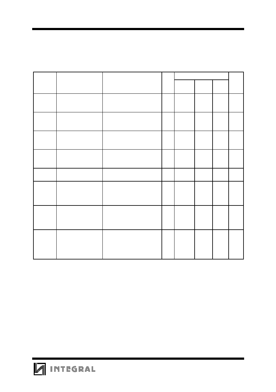
FUNCTION TABLE
Clock
Clock
Enable
Reset
Output State *
L
X
L
no change
X
H
L
no change
X
X
H
reset counter
Q0=H, Q1-Q9=L,
C0=H
L
L
Advance to next
state
X
L
no change
X
L
no change
H
L
Advance to next
state
* Carry Out=H for Q0,Q1,Q2,Q3 or Q4=H
Carry Out = L otherwise, X=don't care

IW4017B
30
MAXIMUM RATINGS
*
Symbol
Parameter
Value
Unit
V
CC
DC Supply Voltage (Referenced to GND)
-0.5 to +20
V
V
IN
DC Input Voltage (Referenced to GND)
-0.5 to V
CC
+0.5
V
V
OUT
DC Output Voltage (Referenced to GND)
-0.5 to V
CC
+0.5
V
I
IN
DC Input Current, per Pin
±
10
mA
P
D
Power Dissipation in Still Air, Plastic DIP+
SOIC Package+
750
500
mW
P
D
Power Dissipation per Output Transistor
100
mW
Tstg
Storage Temperature
-65 to +150
∞
C
T
L
Lead Temperature, 1 mm from Case for 10 Seconds
(Plastic DIP or SOIC Package)
260
∞
C
*
Maximum Ratings are those values beyond which damage to the device may occur.
Functional operation should be restricted to the Recommended Operating Conditions.
+Derating - Plastic DIP: - 10 mW/
∞
C from 65
∞
to 125
∞
C
SOIC Package: : - 7 mW/
∞
C from 65
∞
to 125
∞
C
RECOMMENDED OPERATING CONDITIONS
Symbol
Parameter
Min
Max
Unit
V
CC
DC Supply Voltage (Referenced to GND)
3.0
18
V
V
IN
, V
OUT
DC Input Voltage, Output Voltage (Referenced to GND)
0
V
CC
V
T
A
Operating Temperature, All Package Types
-55
+125
∞
C
This device contains protection circuitry to guard against damage due to high static voltages or electric
fields. However, precautions must be taken to avoid applications of any voltage higher than maximum rated
voltages to this high-impedance circuit. For proper operation, V
IN
and V
OUT
should be constrained to the range
GND
(V
IN
or V
OUT
)
V
CC
.
Unused inputs must always be tied to an appropriate logic voltage level (e.g., either GND or V
CC
).
Unused outputs must be left open.
IW4017B
31
DC ELECTRICAL CHARACTERISTICS
(Voltages Referenced to GND)
V
CC
Guaranteed Limit
Symbol
Parameter
Test Conditions
V
-55
∞
C
25
∞
C
125
∞
C
Unit
V
IH
Minimum High-Level
Input Voltage
V
OUT
=0.5V or V
CC
- 0.5V
V
OUT
=1.0V or V
CC
- 1.0V
V
OUT
=1.5V or V
CC
- 1.5V
5.0
10
15
3.5
7
11
3.5
7
11
3.5
7
11
V
V
IL
Maximum Low -Level
Input Voltage
V
OUT
=0.5V or V
CC
- 0.5V
V
OUT
=1.0V or V
CC
- 1.0V
V
OUT
=1.5V or V
CC
- 1.5V
5.0
10
15
1.5
3
4
1.5
3
4
1.5
3
4
V
V
OH
Minimum High-Level
Output Voltage
V
IN
=GND or V
CC
5.0
10
15
4.95
9.95
14.95
4.95
9.95
14.95
4.95
9.95
14.95
V
V
OL
Maximum Low-Level
Output Voltage
V
IN
=GND or V
CC
5.0
10
15
0.05
0.05
0.05
0.05
0.05
0.05
0.05
0.05
0.05
V
I
IN
Maximum Input
Leakage Current
V
IN
= GND or V
CC
18
±
0.1
±
0.1
±
1.0
µ
A
I
CC
Maximum Quiescent
Supply Current
(per Package)
V
IN
= GND or V
CC
5.0
10
15
20
5
10
20
100
5
10
20
100
150
300
600
3000
µ
A
I
OL
Minimum Output Low
(Sink) Current
V
IN
= GND or V
CC
U
OL
=0.4 V
U
OL
=0.5 V
U
OL
=1.5 V
5.0
10
15
0.64
1.6
4.2
0.51
1.3
3.4
0.36
0.9
2.4
mA
I
OH
Minimum Output
High (Source) Current
V
IN
= GND or V
CC
U
OH
=2.5 V
U
OH
=4.6 V
U
OH
=9.5 V
U
OH
=13.5 V
5.0
5.0
10
15
-2.0
-0.64
-1.6
-4.2
-1.6
-0.51
-1.3
-3.4
-1.15
-0.36
-0.9
-2.4
mA

IW4017B
32
AC ELECTRICAL CHARACTERISTICS
(C
L
=50pF, R
L
=200k
, Input t
r
=t
f
=20 ns)
V
CC
Guaranteed Limit
Symbol
Parameter
V
-55
∞
C
25
∞
C
125
∞
C
Unit
f
max
Maximum Clock Frequency
5.0
10
15
2.5
5
5.5
2.5
5
5.5
1.25
2.5
2.75
MHz
t
PLH
, t
PHL
Maximum Propagation Delay, Clock to Decode
Output (Figure 1)
5.0
10
15
650
270
170
650
270
170
1300
540
340
ns
t
PLH
, t
PHL
Maximum Propagation Delay, Clock to Carry
Output (Figure 1)
5.0
10
15
600
250
160
600
250
160
1200
500
320
ns
t
TLH
, t
THL
Maximum Output Transition Time, Carry
Output or Decode Output (Figure 1)
5.0
10
15
200
100
80
200
100
80
400
200
160
ns
t
PLH
, t
PHL
Maximum Propagation Delay, Reset to Carry
Output or Decode Output (Figure 1)
5.0
10
15
530
230
170
530
230
170
1060
460
340
ns
C
IN
Maximum Input Capacitance
-
5
pF
TIMING REQUIREMENTS
(V
CC
=5.0V
±
10%, C
L
=50pF, Input t
r
=t
f
=20 ns, R
L
=200k
)
V
CC
Guaranteed Limit
Symbol
Parameter
V
-55
∞
C
25
∞
C
125
∞
C
Unit
t
w
Minimum Pulse Width, Clock (Figure 1)
5.0
10
15
200
90
60
200
90
60
400
180
120
ns
t
r,
t
f
Maximum Input Rise and Fall Times, Clock
(Figure 1)
5.0
10
15
UNLIMITED
µ
s
t
w
Minimum Pulse Width, Reset (Figure 1)
5.0
10
15
260
110
60
260
110
60
520
220
120
ns
t
rem
Minimum Removal Time, Reset (Figure 1)
5.0
10
15
400
280
150
400
280
150
800
560
300
ns
t
SU
Minimum Setup Time, Clock Inhibit to Clock
(Figure 1)
5.0
10
15
230
100
70
230
100
70
460
200
140
ns

IW4017B
33
Figure 1. Switching Waveforms
Timing diagram
IW4017B
34
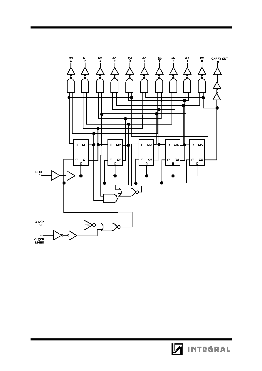
EXPANDED LOGIC DIAGRAM