 | –≠–ª–µ–∫—Ç—Ä–æ–Ω–Ω—ã–π –∫–æ–º–ø–æ–Ω–µ–Ω—Ç: IZ0066 | –°–∫–∞—á–∞—Ç—å:  PDF PDF  ZIP ZIP |

DOT MATRIX LCD CONTROLLER & DRIVER IZ0066
1
1
FEATURES
∑
Internal Memory
-
Character Generator ROM: 8320 bits
-
Character Generator RAM: 512 bit
-
Display Data RAM: 80 x 8 bits for 80 digits
∑
Internal automatic reset circuit at power ON
∑
Internal oscillation circuit
∑
Power Supply Voltage: +5V
±
10%
∑
LCD Driving Voltage for display: 0 ~ -5V(V
5
)
∑
Duty factor selection (selected by programs)
1/8 duty: 5 x 7 dots format 1 line,
1/11 duty: 5 x 10 dots format 1 line
1/16 duty: 5 x 7 dots format 2 line
∑
Bare chip available
∑
Pin-to-Pin replacement for KS0066, HD44780, SED1278
FUNCTION
∑
Character type dot matrix LCD driver & controller
∑
Internal driver: 16 common and 40 segment signal output
∑
Display character format: 5 x 7 dots + cursor,
5 x 10 dots + cursor
∑
Easy interface with a 4-bit or 8-bit MPU
∑
Display character pattern:
5 x 7 dots format: 192 kinds, 5 x 10 dots format: 32 kinds
∑
The special character pattern can be programmable by
Character Generator RAM directly
∑
A customer character pattern can be programmable by mask
option
∑
Wide range of instruction function:
Display clear, Cursor home, Display ON/OFF, Display shift
Cursor ON/OFF, Display character blink, Cursor shift
DESCRIPTION
The IZ0066 is a dot matrix liquid crystal display controller & driver LSI that displays alphanumerics, characters and symbols.
It drives dot matrix LCD under microcomputer control. All functions needed for dot matrix LCD drive are internally provided
on one chip.
ODERING INFORMATION
Type
CGROM
IZ0066 - 00
English
Numberal
Japanese
IZ0066 - 01
English
Numberal
Cyrillic
IZ0066 - XX
Custom font (XX ≠ ROM code)
ABSOLUTE MAXIMUM RATINGS
Characteristic
Symbol
Value
Unit
Power Supply Voltage
V
DD
- 0.3 ~ 7.0
V
Driver Supply Voltage
V
1
~ V
5
V
DD
- 13.5 ~ V
DD
+ 0.3
V
Input Voltage
V
I
-0.3 ~V
DD
+ 0.3
V
Operating Temperature
T
a
- 20 ~ + 75
o
C
Storage Temperature
T
stg
- 55 ~ + 125
o
C
Notes: Must keep the relation of V
DD
V
1
V
2
V
3
V
4
V
5
DOT MATRIX LCD CONTROLLER & DRIVER IZ0066
2
2
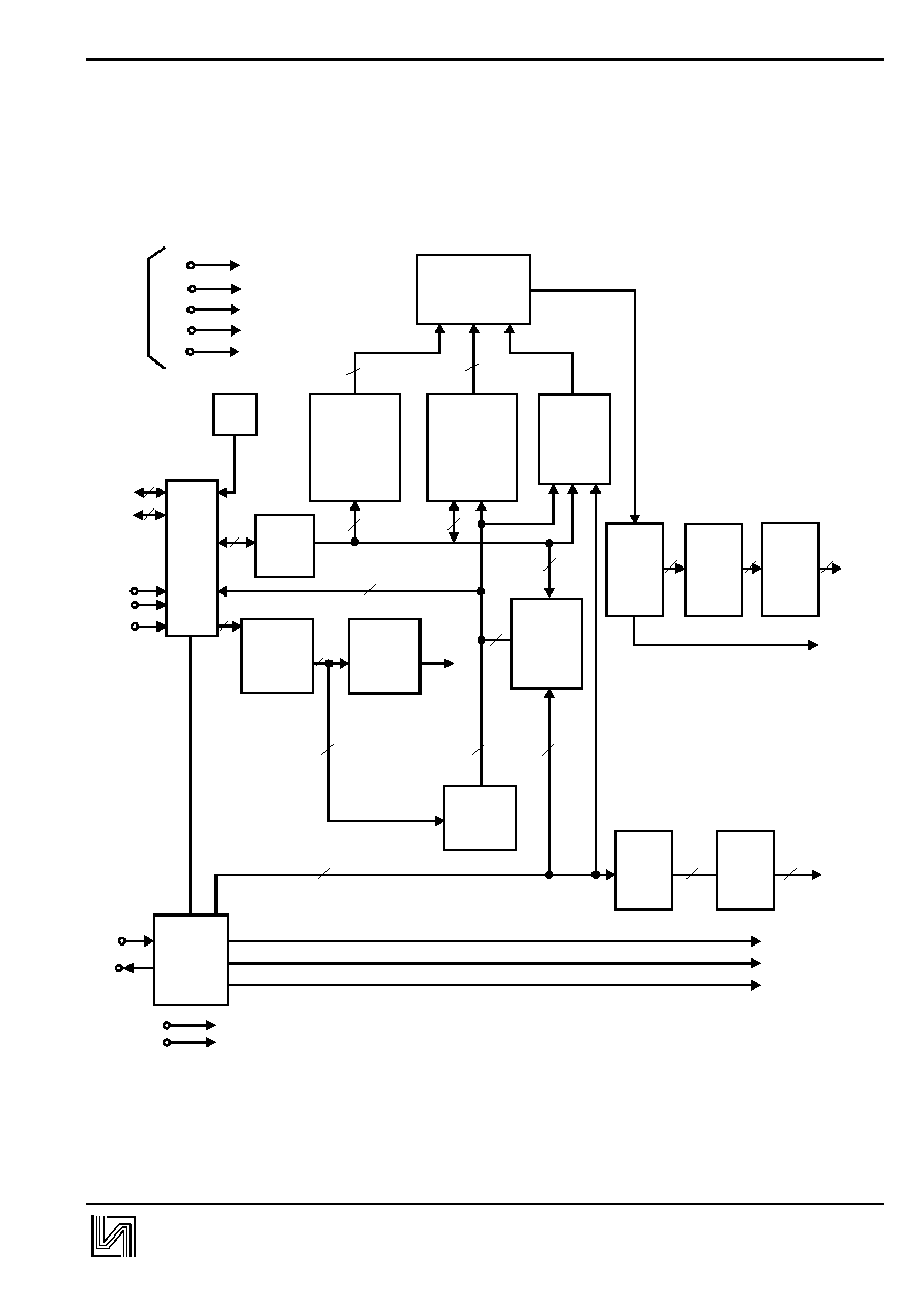
BLOCK DIAGRAM
P arallel/S erial
D ata con v ersion
C ircu it
C h aracter
G en erator
R O M
832 0 b its
C h aracter
G en erator
R A M
512 b its
C u rsor
B lin k
C on trol
C ircu it
D isp lay
D ata R A M
80 x 8 b its
D
T im in g
G en eration
C ircu it
16 - b it
S h ift
R egister
C om m on
S ig n al
D riv er
D ata
R egister
In stru ction
R egister
In stru ction
D ecod er
A d d ress
C ou n ter
I/O
B u ffer
B u sy
F lag
V 1
V 4
V 5
V 3
V 2
P ow er
su p p ly
for
L C D
D riv e
O S C 1
O S C 2
V
S S
V
D D
E
R S
R /W
D B ~D B
0
3
D B ~D B
4
7
4
5
5
4
8
8
8
8
7
7
7
7
16
16
7
4 0 - b it
S h ift
R e g ister
4 0 - b it
L a tch
C ircu it
S e g m en t
S ig n a l
D riv e r
4 0
4 0
4 0
7
8
8
C L K 1
C L K 2
M
C O M 1
to
C O M 16
S E G 1
to
S E G 40
DOT MATRIX LCD CONTROLLER & DRIVER IZ0066
3
3
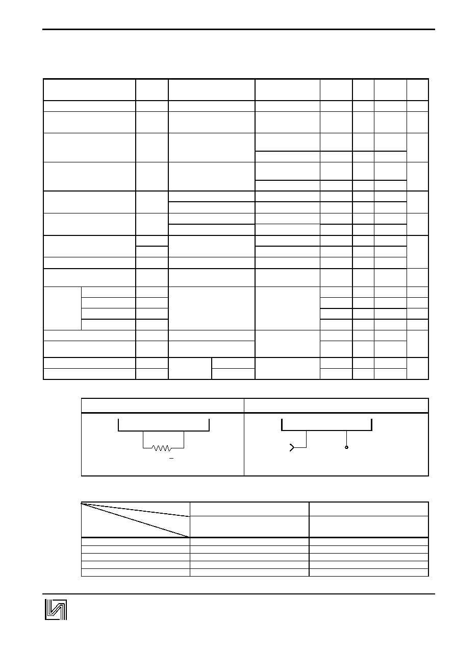
ELECTRICAL CHARACTERISTICS
(Ta = 25
o
C, V
DD
= +5V, V
SS
= 0V unless otherwise specified)
Characteristic
Symbol
Test Condition
Applicable
Terminals
Min
Typ
Max
Unit
Operating Voltage
V
DD
4.5
5.5
V
Operating Current (*1)
I
DD
Internal oscillation or external
clock f
OSC
= 270KHz
0.35
0.6
HIGH Input Voltage
V
IH
E, DB
0
~ DB
7
, R/W,
RS
2.2
V
DD
V
OSC1
V
DD
-1.0
V
DD
LOW Input Voltage
V
IL
E, DB
0
~ DB
7
, R/W,
RS
-0.3
0.6
V
OSC1
-0.2
1.0
HIGH Output Voltage
V
OH
I
OH
= -0.205 mA
DB
0
~ DB
7
2.4
V
I
OH
= -40
µ
A
CLK1, CLK2, M, D
0.9V
DD
LOW Output Voltage
V
OL
I
OL
= 1.2mA
DB
0
~ DB
7
0.4
V
I
OL
= 40
µ
A
CLK1, CLK2, M, D
0.1V
DD
Driver Voltage Descending
V
COM
I
O
=
±
0.1mA
COM1 ~ COM16
1.0
V
V
SEG
SEG1 ~ SEG40
1.0
Input Leakage Current
I
LKG
V
IN
=0V ~ V
DD
E
-1
1
µ
A
Input LOW Current
I
IL
V
CC
= 5V (test pull up R)
RS, R/W, DB
0
~
DB
7
-50
-125
-250
µ
A
Frequency(*1)
f
EC
125
250
350
KHz
External
Duty
DUTY
OSC1
46
50
55
%
Clock
Rise time
t
R
0.2
µ
s
Fall time
t
F
0.2
µ
s
Internal Clock Frequency(*1)
f
OSC1
Rf
= 91K
±
2%
OSC1, OSC2
190
270
350
KHz
Ceramic Resonator Oscillation
Frequency (*1)
f
OSC2
245
250
255
LCD Driving Voltage (*2)
V
LCD1
V
DD
≠ V
5
1/5 bias
V
1
~ V
5
4.6
10.0
V
V
LCD2
1/4 bias
3.0
10.0
Notes: *1). Oscillation circuit
Resistor circuit
External clock circuit
*2). Input the voltage listed in table below to V
1
~ V
5
Duty
1/8, 1/11
1/16
Bias
Power supply
1/4
1/5
V
1
V
DD
≠ V
LCD
/4
V
DD
≠ V
LCD
/5
V
2
V
DD
≠ V
LCD
/2
V
DD
≠ 2V
LCD
/5
V
3
V
DD
≠ V
LCD
/2
V
DD
≠ 3V
LCD
/5
V
4
V
DD
≠ 3V
LCD
/4
V
DD
≠ 4V
LCD
/5
V
5
V
DD
≠ V
LCD
V
DD
≠ V
LCD
*V
LCD
is the LCD driving voltage, refer to the initial set of the instruction code.
O S C 1
O S C 2
op en
F req u en cy inp u t
O S C 1
R f
R f: 91k
+ 2%
O S C 2

DOT MATRIX LCD CONTROLLER & DRIVER IZ0066
4
4
AC CHARACTERISTICS
(V
DD
= 5V, V
SS
= 0V, Ta = 25
o
C)
(1) Write mode (Writing data from MPU to IZ0066)
Characteristic
Symbol
Test pin
Min
Typ
Max
Unit
E Cycle Time
t
C
E
500
ns
E Rise Time
t
R
E
25
ns
E Fall Time
t
F
E
25
ns
E Pulse Width (High, Low)
t
W
E
220
ns
R/W and RS Set-up Time
t
SU1
R/W, RS
40
ns
R/W and RS Hold Time
t
H1
R/W, RS
10
ns
Data Set-up Time
t
SU2
DB
0
~ DB
7
60
ns
Data Hold Time
t
H2
DB
0
~ DB
7
10
ns
(2) Read mode (Reading data from IZ0066 to MPU)
Characteristic
Symbol
Test pin
Min
Typ
Max
Unit
E Cycle Time
t
C
E
500
ns
E Rise Time
t
R
E
25
ns
E Fall Time
t
F
E
25
ns
E Pulse Width (High, Low)
t
W
E
220
ns
R/W and RS Set-up Time
t
SU1
R/W, RS
40
ns
R/W and RS Hold Time
t
H1
R/W, RS
10
ns
Data Output Delay Time
t
D
DB
0
~ DB
7
120
ns
Data Hold Time
t
H2
DB
0
~ DB
7
20
ns
R S
R / W
E
D B ~ D B
0
7
V
IH 1
V
IH 1
V
IH 1
V
IH 1
V
IL 1
V
IL 1
V
IL 1
V
IL 1
V
IL 1
V
IL 1
V
IL 1
t
S U 1
t
S U 2
t
W
t
H 1
t
H 1
t
H 2
t
R
t
C
V alid D ata

DOT MATRIX LCD CONTROLLER & DRIVER IZ0066
5
5
(3) Interface mode with IZ0065
Characteristic
Symbol
Test pin
Min
Typ
Max
Unit
Clock Pulse Width High
t
WCKH
CLK
800
ns
Clock Pulse Width Low
t
WCKL
CLK
800
ns
Data Set-up Time
t
SU
D
300
ns
Data Hold Time
t
DH
D
300
ns
Clock Set-up Time
t
CSU
CLK
500
ns
M Delay Time
t
DM
M
-1000
1000
ns
R S
R / W
E
D B ~ D B
0
7
V
IH 1
V
IH 1
V
IH 1
V
IH 1
V
IH 1
V
IL 1
V
IL 1
V
IL 1
V
IL 1
V
IL 1
V
IL 1
V
IL 1
V
IL 1
t
S U
t
W
t
H
t
H
t
D H
t
D
t
R
t
C
V alid D ata
t
F
C L K 1
C L K 2
D
M
0.9V
D D
0.9V
D D
0.9V
D D
0.9V
D D
0.1V
D D
0.1V
D D
0.1V
D D
0.1V
D D
0.1V
D D
0.9V
D D
0.9V
D D
0.9V
D D
t
S U
t
D M
t
D M
t
W C K 1
t
C S U
t
C S U
t
W C K H
t
W C K H
DOT MATRIX LCD CONTROLLER & DRIVER IZ0066
6
6
TERMINAL DESCRIPTION
Pin
INPUT/OUTPUT
Name
DESCRIPTION
INTERFACE
V
DD
Operating Voltage
For logical circuit (+5V
±
10%)
Power
V
SS
Power
0V(GND)
Supply
V
1
≠ V
5
Negative Supply Voltage
Bias voltage level for LCD driving
SEG1≠ SEG40
Output
Segment output
Segment signal output for LCD driving
LCD
COM1≠ COM16
Output
Common output
Common signal output for LCD driving
LCD
OSC1
OSC2
Input
Output
Oscillator
Both pin connected to Rf resistor or ceramic
resonator for internal oscillator circuit. In case of
external frequency use only, the frequency is input
to OSC1 terminal.
Resistor or
Ceramic
Resonator
CLK1
Data latch clock
Clock output terminal for the serially transferred
data to be latched to the driver.
CLK2
Output
Data shift clock
Clock output terminal used when D terminal data
output shifts the inside of the driver.
IZ0065
M
Alternated signal for LCD
driver output
The alternating signal to convert LCD drive
waveform to AC.
Character pattern data, which is corresponding to
each common signal, is supplied to driver serially.
High
Selection
Low
Non selection
D
Display data interface
E
Input
Enable
Start anable signal to read or write the data
MPU
R/W signal input is used to select the read/write
mode
High
Read mode
Low
Write mode
R/W
Read/Write
Register selection input
High
Data register (for read
and write)
Low
Instruction register (for
write), Busy flag, address
counter (for read)
RS
Register select
DB
0
≠ DB
7
Input/Output
Data interface
Used for data transfer between the MPU and
IZ0066. These terminals are for data bus with
bidirectional three-state.
Initial 4 bit (DB
0
-DB
3
) are not used during 4 bit
operation (DB
7
can be used as a busy flag)

DOT MATRIX LCD CONTROLLER & DRIVER IZ0066
7
7
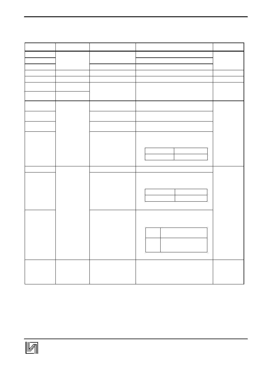
CONTROL and DISPLAY COMMANDS
Command
RS
R/W
DB
7
DB
6
DB
5
DB
4
DB
3
DB
2
DB
1
DB
0
Execution time
(f
OSC
=250KHz)
Remark
DISPLAY
CLEAR
L
L
L
L
L
L
L
L
L
H
1.64 ms
RETURN
HOME
L
L
L
L
L
L
L
L
H
X
1.64 ms
Cursor move to first digit
ENTRY
MODE SET
L
L
L
L
L
L
L
H
I/D
SH
40
µ
s
*I/D: set cursor move
direction
*SH: Specifies shift of
display
DISPLAY
ON/OFF
L
L
L
L
L
L
H
D
C
B
40
µ
s
*Display
*Cursor
*Blinking
SHIFT
L
L
L
L
L
H
S/C
R/L
X
X
40
µ
s
SET
FUNCTION
L
L
L
L
H
DL
N
F
X
X
40
µ
s
SET CG
RAM
ADDRESS
L
L
L
H
CG RAM address (corresponds to
cursor address)
40
µ
s
CG RAM Data is sent and
received after this setting
SET DD
RAM
ADDRESS
L
L
H
DD RAM address
40
µ
s
DD RAM Data is sent and
received after this setting
READ BUSY
FLAG &
ADDRESS
L
H
BF
Address Counter used for Both DD &
CG RAM address
0
µ
s
-Reads BF indication
internal operating
is being performed.
-Reads address
counter contents
WRITE
DATA
H
L
Write Data
46
µ
s
Write data DD or CG RAM
READ DATA
H
H
Read Data
46
µ
s
Read data from DD or CG
RAM
Note: X ≠ Don't care.
SH
H
Display is
shifted
L
Display is not
shifted
I/D
H
Increase
L
Decrease
D
H
Display on
L
Display off
C
H
Cursor on
L
Cursor off
B
H
Blinking on
L
Blinking off
SC
H
Display shift
L
Cursor move
R/L
H
Right shift
L
Left shift
DL
H
8 bits interface
L
4 bits interface
N
H 2 line display
L
1 line display
F
H
5x10 dots
L
5x7 dots
BF
H
Busy
L
Ready
DOT MATRIX LCD CONTROLLER & DRIVER IZ0066
8
8
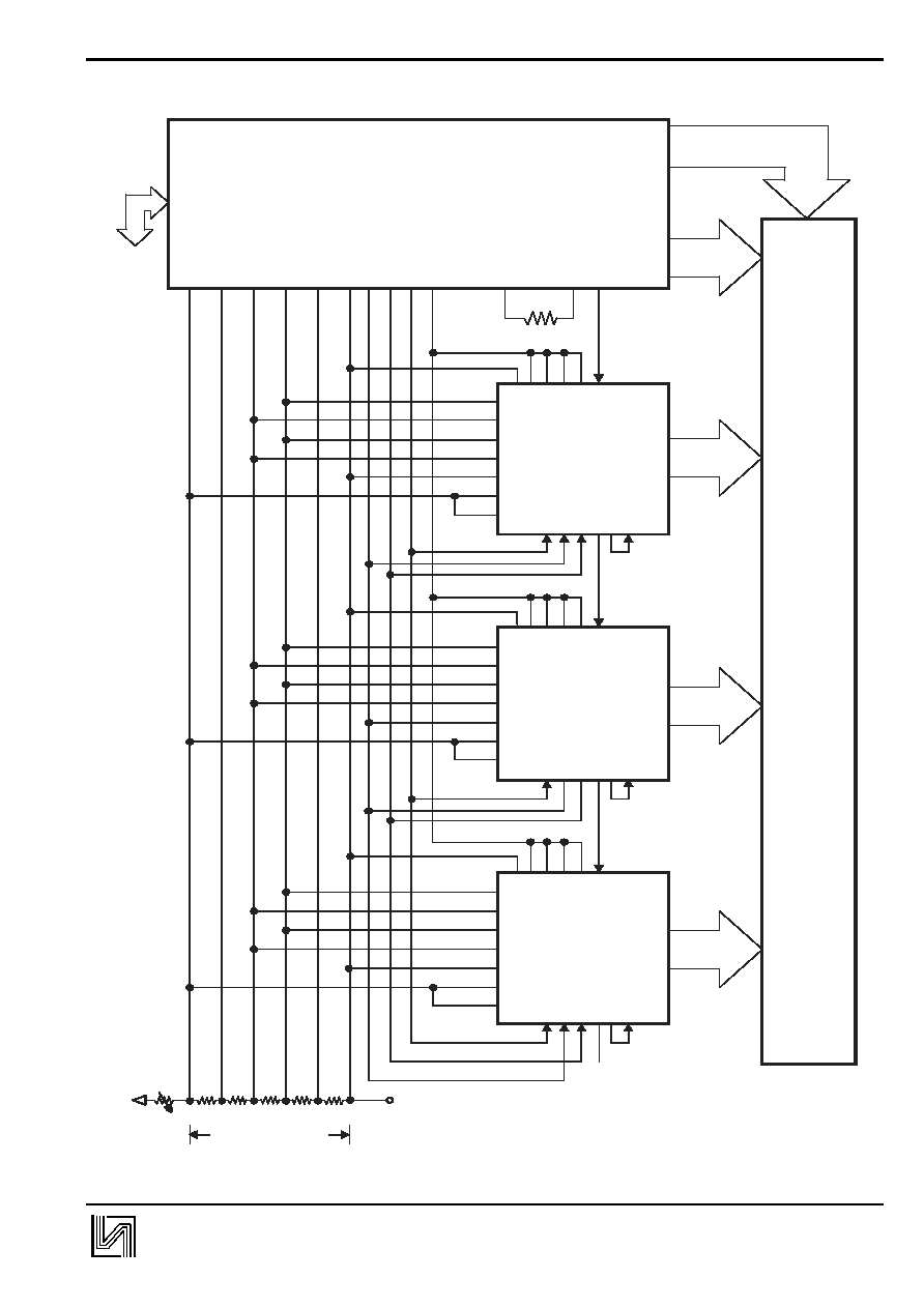
APPLICATION CIRCUIT
When IZ0065 is externally connected to the IZ0066, you can increase the number of display digits up to 80 characters.
I
Z
006
6
V
(1 /5 b ia s)
LC D
LC
D
Pa
n
e
l
CO
M
1
~
C
O
M
1
6
SE
G
1
~
S
E
G
4
0
D
OS
C1
OS
C
2
V
SS
M
CL
K
1
CL
K
2
V
DD
V
1
V
2
V
3
V
4
V
5
DB
~
DB
07
SC
~
SC
14
0
SC
~
SC
14
0
SC
~
SC
14
0
DL
2
DR
1
DR
2
CL
1
CL
2
M
DL
2
DR
1
DR
2
CL
1
CL
2
M
DL
2
DR
1
DR
2
CL
1
CL
2
M
V
EE
V
1
V
2
V
3
V
4
V
5
V
6
V
EE
V
1
V
2
V
3
V
4
V
5
V
6
V
EE
V
1
V
2
V
3
V
4
V
5
V
6
V
DD
V
SS
SH
L
2
SH
L
1
FC
S
DL
1
V
DD
V
SS
SH
L
2
SH
L
1
FC
S
DL
1
V
DD
V
SS
SH
L
2
SH
L
1
FC
S
DL
1
I
Z
006
5
I
Z0
0
6
5
I
Z0
0
6
5
V
DD
V
5
V
4
V
3
V
2
V
1
GN
D
or
ot
he
r
vo
l
t
age
To M PU
DOT MATRIX LCD CONTROLLER & DRIVER IZ0066
9
9
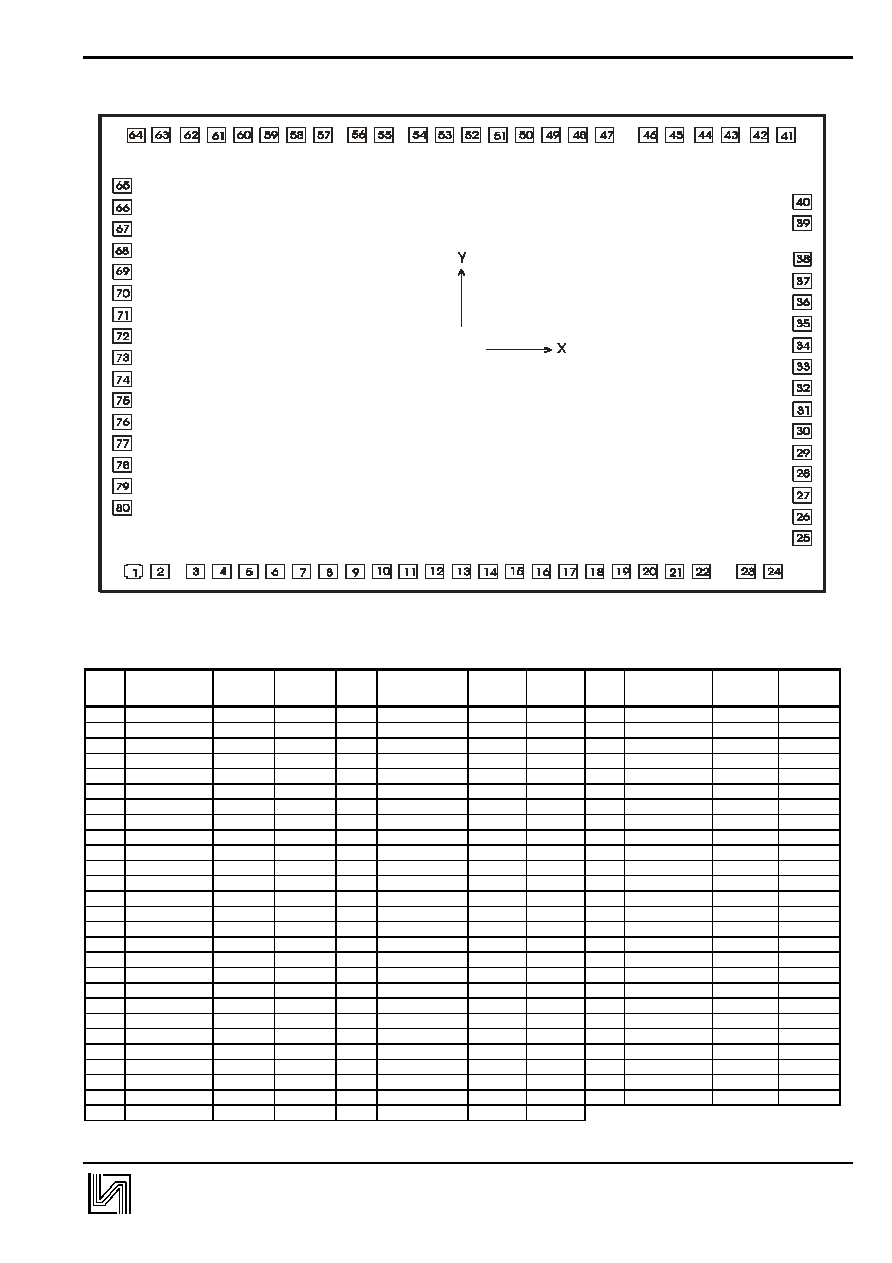
PAD LAYOUT
The chip substrate is connected to V
DD
.
PAD LOCATION
( Unit:
µ
m)
Pad
No.
Pad Name
X
Y
Pad
No.
Pad Name
X
Y
Pad
No.
Pad Name
X
Y
1
SEG22
-2221
-1830
28
V3
2299
-1012
55
COM9
-530
1830
2
SEG21
-2041
-1830
29
V4
2299
-832
56
COM10
-710
1830
3
SEG20
-1804
-1830
30
V5
2299
-862
57
COM11
-941
1830
4
SEG19
-1624
-1830
31
CL1
2299
-472
58
COM12
-1121
1830
5
SEG18
-1444
-1830
32
CL2
2299
-292
59
COM13
-1301
1830
6
SEG17
-1264
-1830
33
V
CC
2299
-112
60
COM14
-1481
1830
7
SEG16
-1084
-1830
34
M
2299
68
61
COM15
-1661
1830
8
SEG15
-904
-1830
35
D
2299
248
62
COM16
-1841
1830
9
SEG14
-724
-1830
36
RS
2299
428
63
SEG40
-2036
1830
10
SEG13
-544
-1830
37
R/W
2299
608
64
SEG39
-2216
1830
11
SEG12
-364
-1830
38
E
2299
788
65
SEG38
-2298
1404
12
SEG11
-184
-1830
39
DB0
2299
1090
66
SEG37
-2298
1224
13
SEG10
-4
-1830
40
DB1
2299
1270
67
SEG36
-2298
1044
14
SEG9
176
-1830
41
DB2
2188
1830
68
SEG35
-2298
864
15
SEG8
35
-1830
42
DB3
2008
1830
69
SEG34
-2298
684
16
SEG7
536
-1830
43
DB4
1812
1830
70
SEG33
-2298
504
17
SEG6
716
-1830
44
DB5
1632
1830
71
SEG32
-2298
324
18
SEG5
896
-1830
45
DB6
1436
1830
72
SEG31
-2298
144
19
SEG4
1076
-1830
46
DB7
1256
1830
73
SEG30
-2298
-36
20
SEG3
1256
-1830
47
COM1
961
1830
74
SEG29
-2298
-216
21
SEG2
1436
-1830
48
COM2
781
1830
75
SEG28
-2298
-396
22
SEG1
1616
-1830
49
COM3
601
1830
76
SEG27
-2298
-576
23
GND
1920
-1830
50
COM4
421
1830
77
SEG26
-2298
-756
24
OSC1
2100
-1830
51
COM5
241
1830
78
SEG25
-2298
-936
25
OSC2
2299
-1552
52
COM6
61
1830
79
SEG24
-2298
-1116
26
V1
2299
-1372
53
COM7
-119
1830
80
SEG23
-2298
-1296
27
V2
2299
-1192
54
COM8
-299
1830
(0 ,0 )
IZ0 0 6 6 PA D D IA G R A M
C h ip size : 4 0 0 0 x 4 9 0 0
Pa d size : 1 2 0 x 1 2 0
U n it : m
µ