 | –≠–ª–µ–∫—Ç—Ä–æ–Ω–Ω—ã–π –∫–æ–º–ø–æ–Ω–µ–Ω—Ç: LD1207 | –°–∫–∞—á–∞—Ç—å:  PDF PDF  ZIP ZIP |

1
TECHNICAL DATA
LD1207
DESCRIPTION
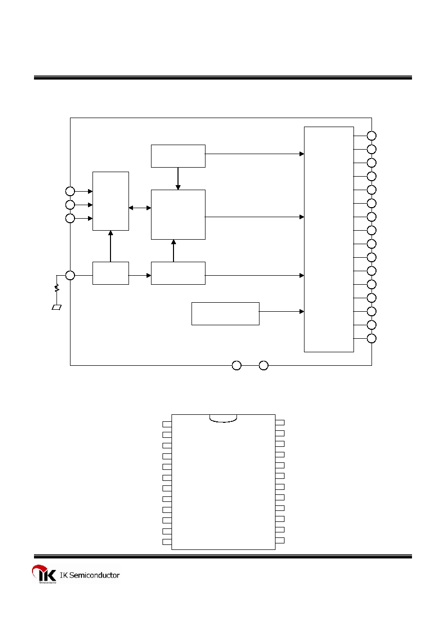
The LD1207 is specifically designed for LED and LED DISPLAY derivers.
The LD1207 have 12/9 segment output lines, 7 to 4 grid output lines, one display memory, control circuit
and 3 line serial data interface.
This function are all incorporated into a single chip to build a highly reliable peripheral
device for a single chip microcomputer. It is very convenience to control for numeric display.
LD1207's pin assignments and application circuit are optimized for easy PCB Layout and cost saving
advantages.
FEATURES
∑ CMOS Technology
∑ Segment output line selection by command : 12 ~ 9
∑ Grid output line selection by command : 7 ~ 4
∑ Operation voltage : 5V
∑ Low Power Consumption
∑ 8-Step Dimming control by command
∑ Serial Interface for Clock, Data Input, Strobe Pins
∑ 24-pin, SOP Package
APPLICATION
∑ Segment LED display : VCR, DVD, MWO

2
TECHNICAL DATA
LD1207
BLOCK DIAGRAM
Segment
Driver /
Grid Driver
Serial
Data
Interface
OSC
Display
Memory
Control
Timing
Generator
Dimming Circuit
SG1
SG2
SG3
PIN CONFIGURATION
SG4
DIN
SG5
SG6
VDD
CLK
STB
SG7
SG8
SG9
SG10/GR7
SG11/GR6
R
OSC
SG12/GR5
GR4
GR3
GND
GR2
GR1
GND
GND
VDD
SG12/GR5
SG11/GR6
SG10/GR7
SG9
SG8
GND
GR1
GR2
GR3
GR4
SG1
SG2
SG3
SG4
SG5
SG6
SG7
OSC
DIN
CLK
STB
VDD
6
7
8
9
10
11
12
1
2
3
4
5
19
18
17
16
15
14
13
24
23
22
21
20

3
TECHNICAL DATA
LD1207
PIN DESCRIPTION
Pin Name
OSC
DIN
CLK
STB
VDD
SG1 to SG9
SG10/GR7 to
SG12/GR5
GND
GR4 to GR1
I/O
I
I
I
I
-
O
O
-
O
Description
Pin No.
Oscillator Input Pin.
A resistor is connected to this pin and GND.
1
Data Input Pin.
This pin inputs serial data at the rising edge of
the shift clock (staring from the lower bit)
2
Clock Input Pin.
Rising edge trigger.
3
Strobe pin for Serial Interface.
The data input after the STB has fallen is
processed as a command.
When this pin is "HIGH", CLK is ignored.
4
Power Supply
5,18
Segment Output Pins(p-channel, open drain)
6~14
Segment Output Pin/ Grid Output Pin
(CMOS Output)
15~17
Ground Pin
19,24
Grid Output Pins (n-channel, open drain)
20~23

4
TECHNICAL DATA
LD1207
FUNCTIONAL DESCRIPTION
Commands
A command is the first byte (b0 to b7) inputted to LD1207 via DIN Pin after STB Pin has changed from
"HIGH" to "LOW" state. If for some reason the STB Pin is set "HIGH" while data or commands are
being transmitted, the serial communication is initialized, and the data/commands being transmitted are
considered invalid.
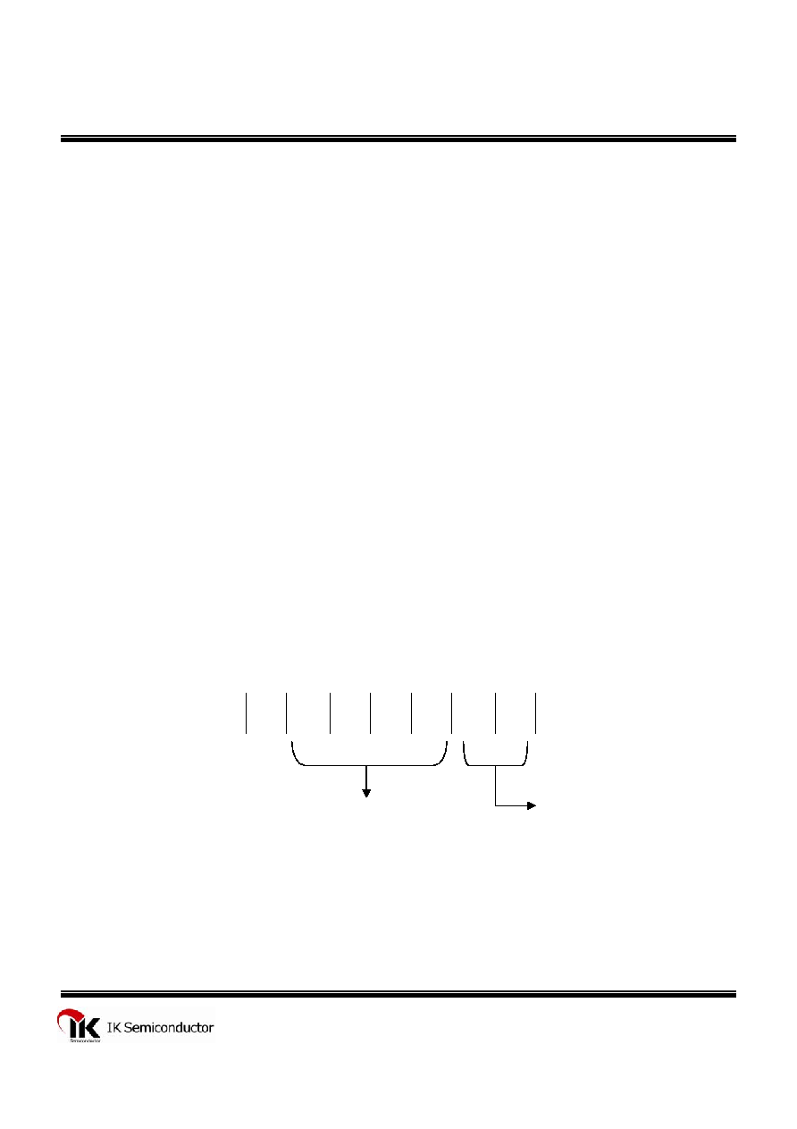
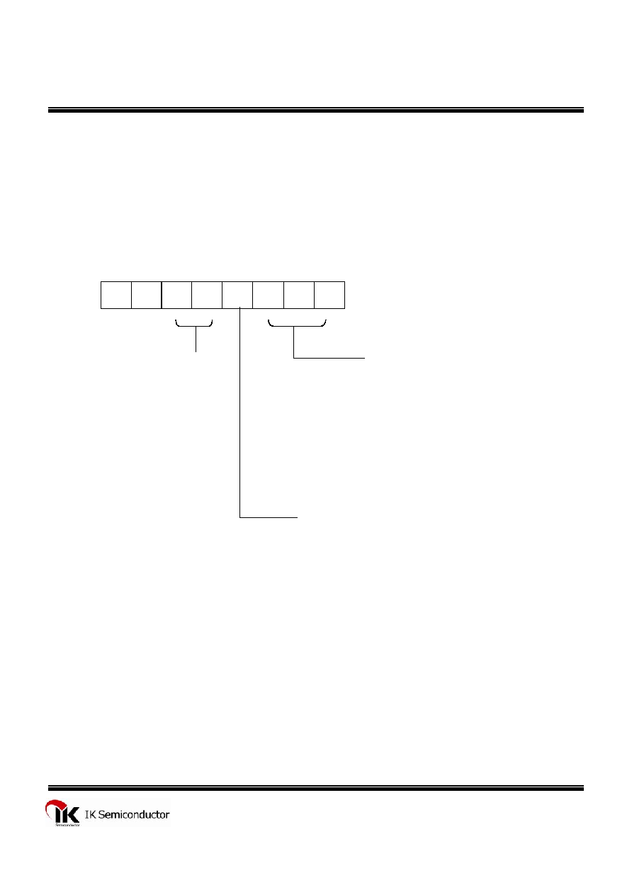
COMMAND 1 : DISPLAYMODE SETTING COMMANDS
LD1207 provides 4 display mode setting as shown in the diagram below: As stated earlier a
command is the first one byte(b0 to b7) transmitted to LD1207 via the DIN Pin when STB is
"LOW". However, for these commands, Bit No.3 to Bit No.6(b2 to b5) are ignored,
Bit No.7 & Bit No.8(b6 to b7) are given a value of "0".
The Display Mode Setting Commands determine the number of segments and grids be used
(1/4 to 1/7 duty, 12 to 9 segments). When these commands are executed, the display forcibly
turned off. A display command "ON" must be executed in order to resume display. If the same
mode setting is selected, no command execution is take place, therefore, nothing happens.
When Power is turned "ON", the 7-Grid, 9-Segment Mode is selected.
LSB
MSB
0
-
-
-
-
b1
b0
0
Display Mode Settings :
00 : 4 Grids, 12 Segments
01 : 5 Grids, 11 Segments
10 : 6 Grids, 10 Segments
11 : 7 Grids, 9 Segments
Don't Care

5
TECHNICAL DATA
LD1207
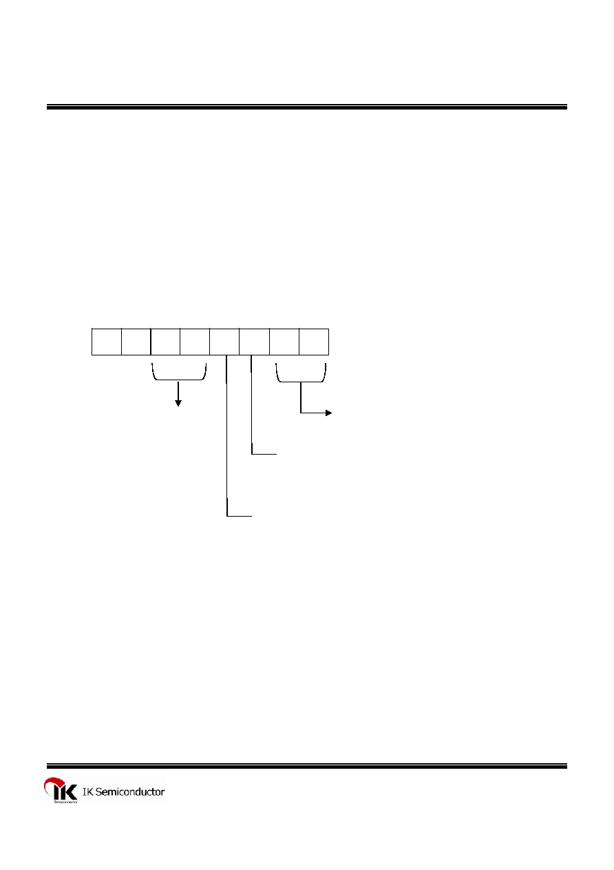
COMMAND 2 : DATA SETTING COMMANDS
The Data Setting Commands executes the Data Write Mode for LD1207. The Data Setting
Command, the bits5 and 6 (b4, b5) are ignored, bit7(b6) is given the value of "1" while bit8(b7) is
given the value of "0". Please refer to the diagram below.
When power is turned ON, bit 4 to bit 1 (b3 to b0) are given the value of "0".
LSB
MSB
0
1
-
-
b3
b2
b1
b0
Data Write Mode Settings :
00 : Write Data to Display Mode
Don't Care
Address Increment Mode Settings (Display Mode):
0 : Increment Address after Data has been Written
1 : Fixes Address
Mode Settings :
0 : Normal Operation Mode
1 : Test Mode

6
TECHNICAL DATA
LD1207
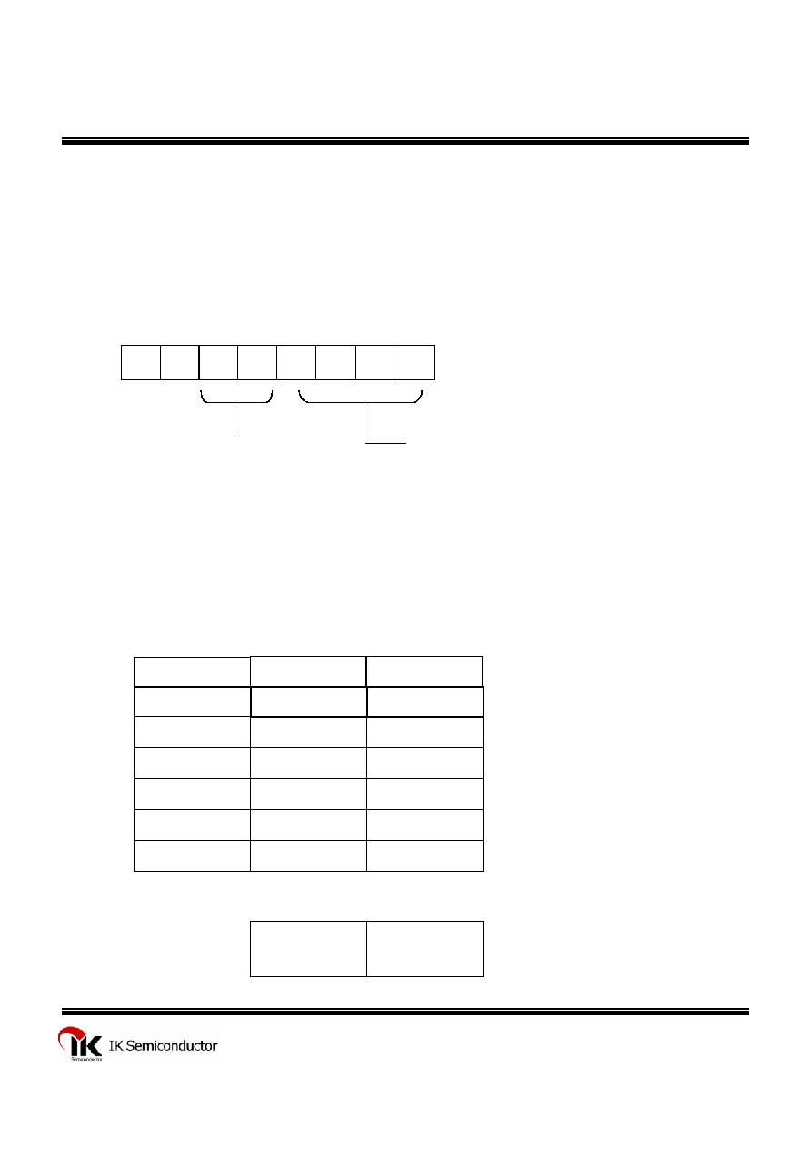
COMMAND 3 : ADDRESS SETTING COMMANDS
Address Setting Commands are used to set the address of the display memory. The address is
considered valid if it has a value of "00H" to 0DH". If the address is set to 0EH or higher, the
data is ignored until a valid address is set. When power is turned ON, the address is set at "00H".
Please refer to the diagram below.
LSB
MSB
1
1
-
-
b3
b2
b1
b0
Address : 00H to 0DH
Don't Care
Display Mode and RAM Address
Data transmitted from an external device to LD1207 via the serial interface are stored in the
Display RAM and are assigned addresses. The RAM Addresses of LD1207 are given below in
8 bit unit.
SG4 SG5
SG8 SG9
SG12
SG1
DIG1
00H
L
04H
U
00H
U
05H
L
01H
L
02H
U
03H
L
02H
L
04H
L
06H
U
07H
L
06H
L
08H
U
09H
L
08H
L
0AH
U
0BH
L
0AH
L
0CH
U
0DH
L
0CH
L
DIG2
DIG3
DIG4
DIG5
DIG6
DIG7
b3
b4
b7
b0
xxH
L
xxH
U
Lower 4 bits Higher 4 bits

7
TECHNICAL DATA
LD1207
COMMAND 4 : DISPLAY CONTROL COMMANDS
The Display Control Commands are used to turn ON or OFF a display. It also used to set the
pulse width. Please refer to the diagram below. When the power is turned ON, a 1/16 pulse
width is selected and the displayed is turned OFF.
LSB
MSB
1
0
-
-
b3
b2
b1
b0
Dimming Quantity Settings :
000 : Pulse width = 1/16
001 : Pulse width = 2/16
010 : Pulse width = 4/16
011 : Pulse width = 10/16
100 : Pulse width = 11/16
101 : Pulse width = 12/16
110 : Pulse width = 13/16
111 : Pulse width = 14/16
Don't Care
Display Settings :
0 : Display OFF
1 : Display ON

8
TECHNICAL DATA
LD1207
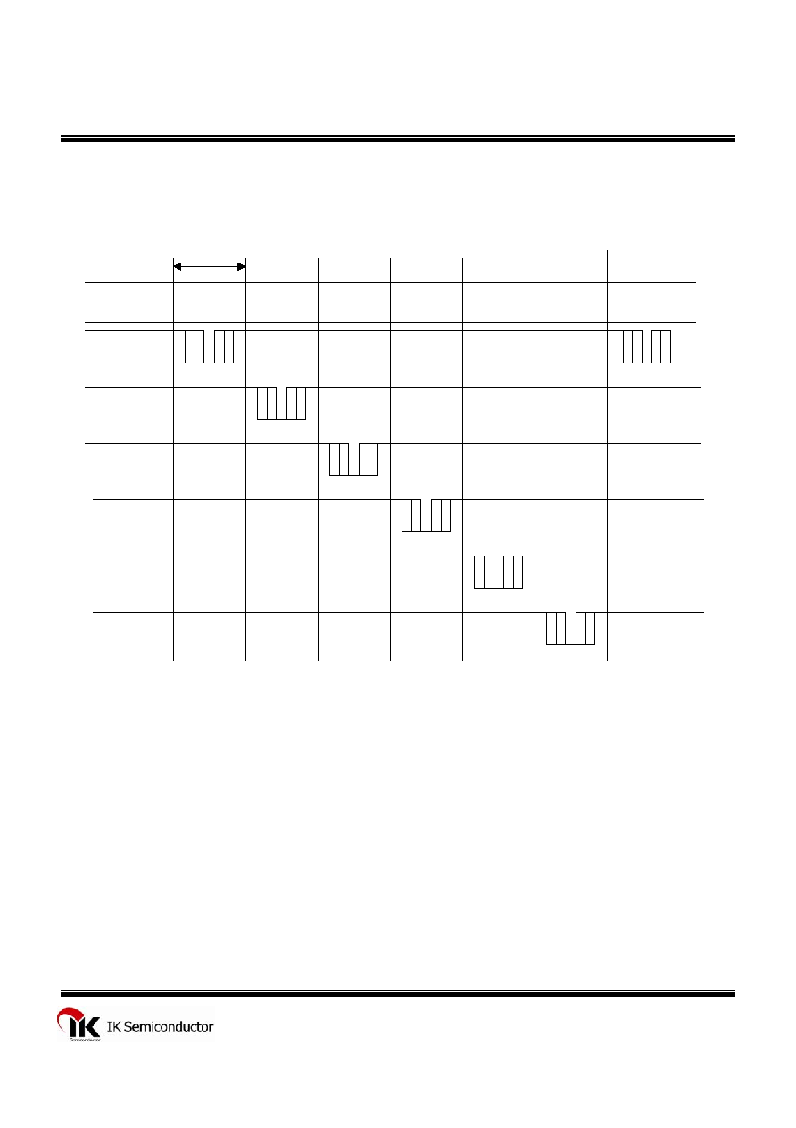
DISPLAY TIMING WAVEFORM
SG Output
DIG1
DIG2
DIG3
DIG4
--------
DIGn
DIG1
G1
G2
G3
G4
Gn
-------
T
DISPLAY
=500us

9
TECHNICAL DATA
LD1207
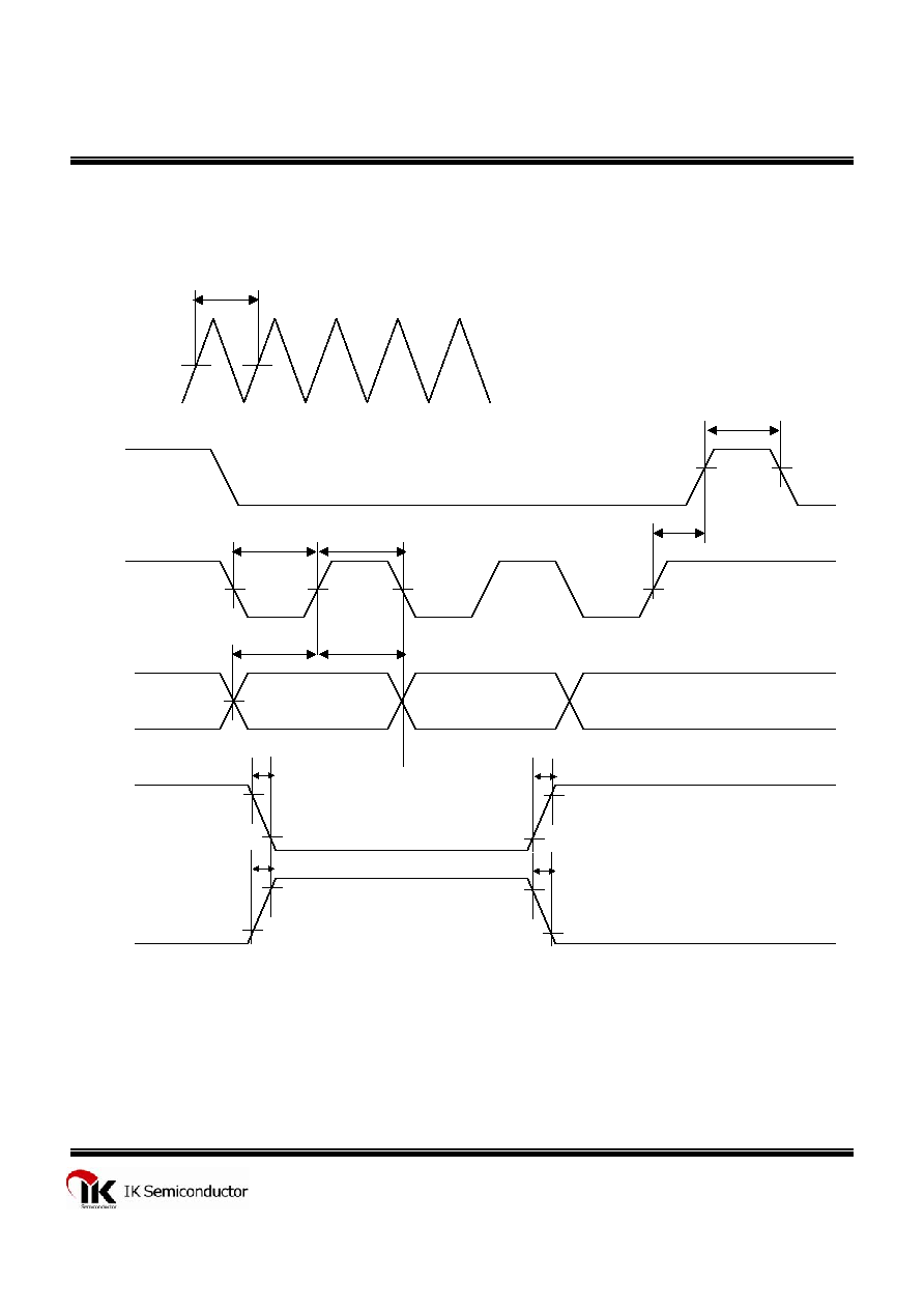
SWITCHING CHARACTERISTIC WAVEFORM
LD1207 Switching Characteristies Waveform is given below.
f
OSC
OSC
PW
STB
STB
CLK
DIN
10%
90%
PW
CLK
t
setup
t
hold
t
CLK-STB
90%
10%
t
TZH
t
TLZ
t
THZ
PW
CLK
t
TZL
Gn
Sn
PW
CLK
(Clock Pulse Width) 400ns
t setup (Data Setup Time) 100ns
t
CLK-STB
(Clock - Strobe Time) 1
t
TZH
(Rise Time) 1
t
TZL
<1
PW
STB
(Strobe Pulse Width) 1
thold (Data Hold Time) 100ns
t
THZ
(Fall Time) 10
fosc = Oscillation Frequency
t
TlZ
<10

10
TECHNICAL DATA
LD1207
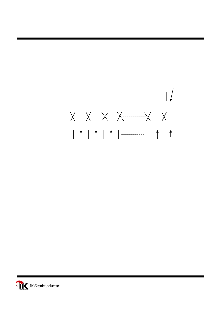
SERIAL COMMUMICATION FORMAT
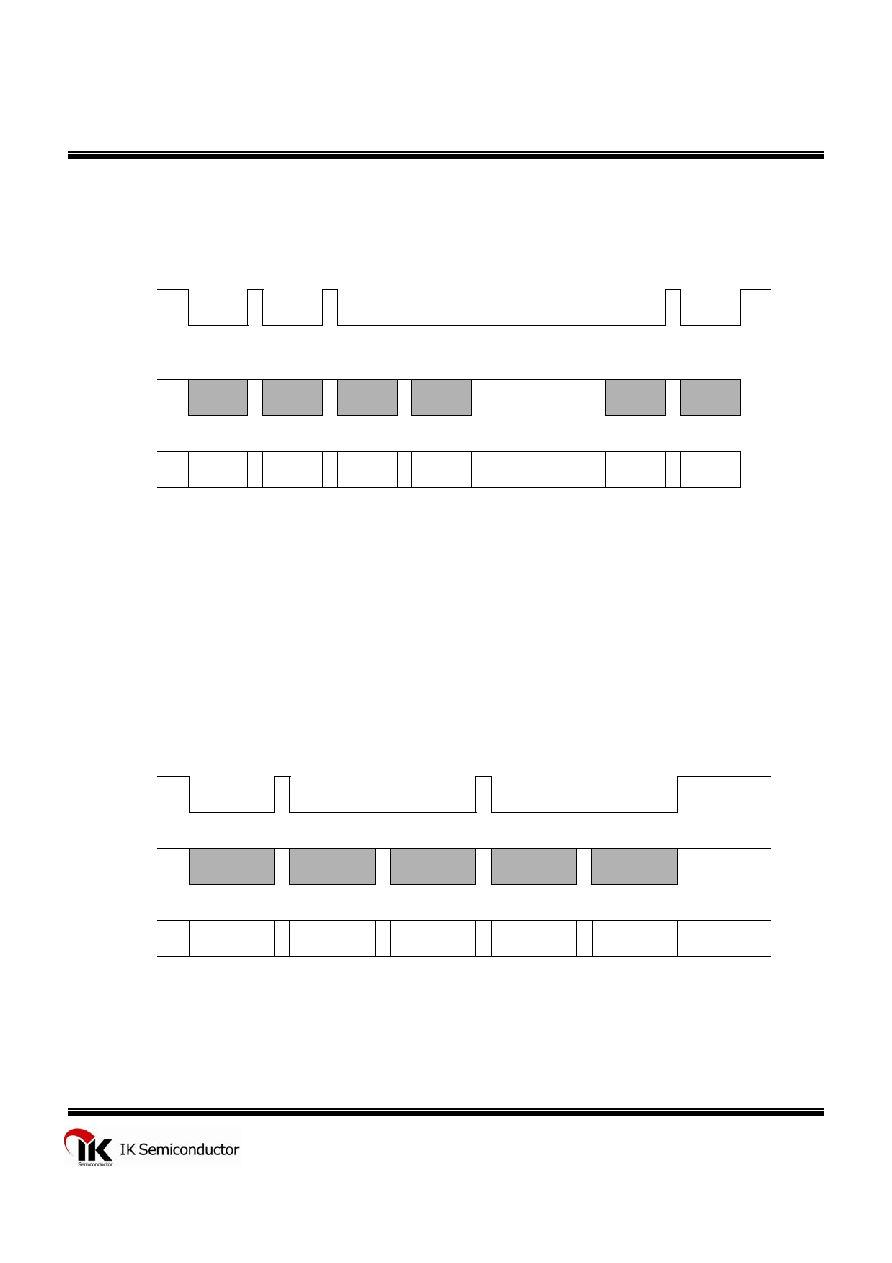
The following diagram shows the LD1207 serial communication format.
RECEPTION (Data/Command Write)
If data continues.
STB
DIN
b0
b1
b2
b6
b7
1
2
3
7
8
CLK

11
TECHNICAL DATA
LD1207
APLICATIONS
Display memory is updated by incrementing addresses. Please refer to the following diagram.
Command1
Command2
Command3
Data1
Data2
Command4
---------------------
---------------------
STB
CLK
DIN
Where : Command 1 : Display Mode Setting
Command 2 : Data Setting Command
Command 3 : Address Setting Command
Data 1 to n : Transfer Display Data (14 Bytes max.)
Command 4 : Display Control Command
The following diagram shows the waveforms when updating specific addresses.
command2
command3
Data
command3
Data
STB
DIN
CLK
Where : Command 2 -- Data Setting Command
Command 3 -- Address Setting Command
Data -- Display Data

12
TECHNICAL DATA
LD1207
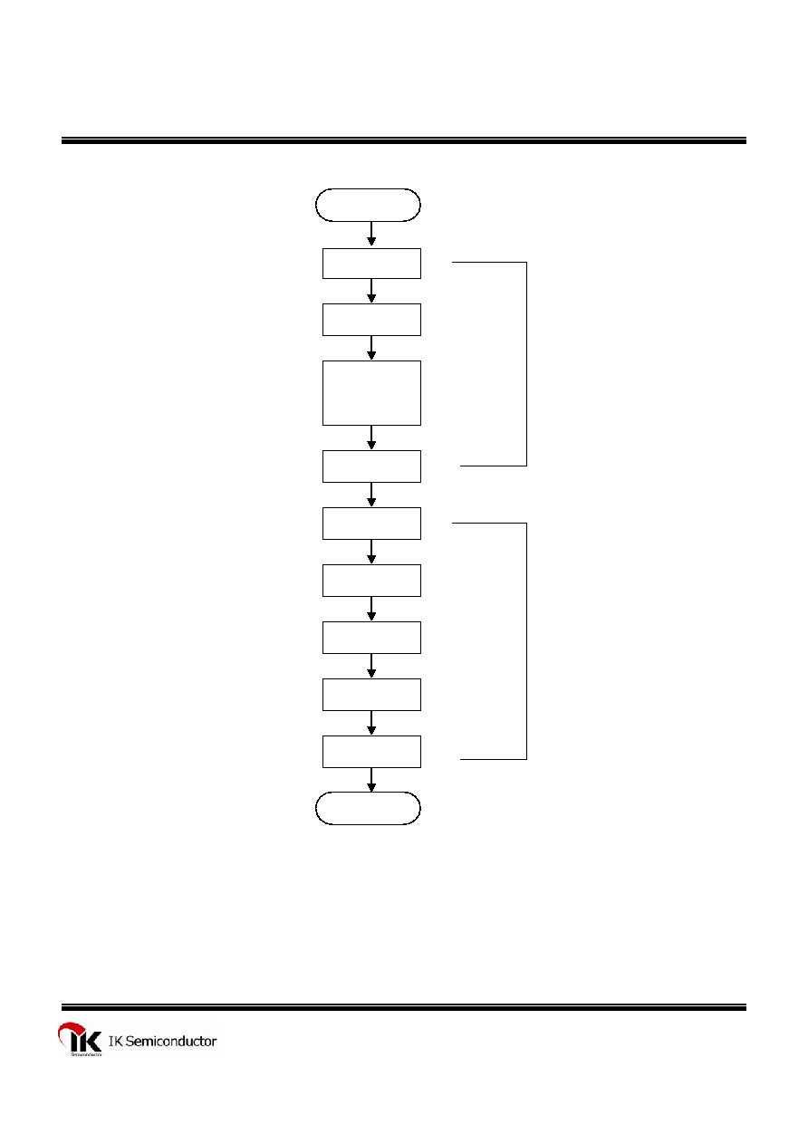
RECOMMENDED SOFTWARE PROGRAMMING FLOWCHART
START
SET
COMMAND 1
SET
COMMAND 2
SET
COMMAND 3
Clear Display RAM
(see Note 5)
SET
COMMAND 4
MAIN
PROGRAM
SET
COMMAND 1
SET
COMMAND2
SET
COMMAND 3
SET
COMMAND 4
INITIAL
SETTING
MAIN
LOOP
END
Note : 1. Command 1 : Display Mode Setting
2. Command 2 : Data Setting Commands
3. Command 3 : Address Setting Commands
4. Command 4 : Display Control Commands
5. When IC power is applied for the first time, the contents of the Display RAM are not defined : thus,
it is strongly suggested that the contents of the Display RAM must be cleared during the initial setting.

13
TECHNICAL DATA
LD1207
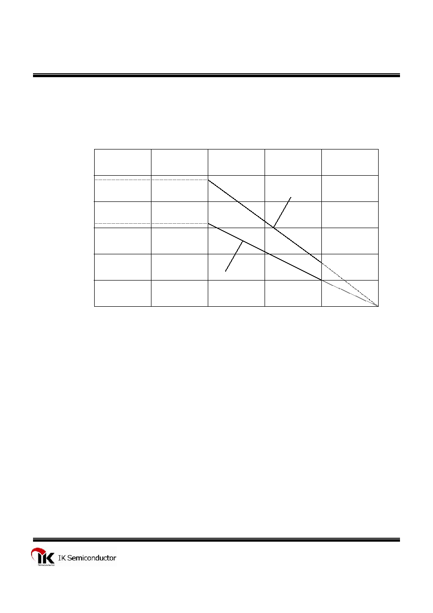
SOP 24L (300 MIL) THERMAL PERFORMANCE IN STILL AIR
Junction Temperature : 100
1200
966
616
IC Mounted Glass Epoxy PCB
IC Single
1000
Power Dissipation, Pd (mW)
800
600
400
200
0
-25
0
25
50
75
100
Ambient Temperature, Ta (
)

14
TECHNICAL DATA
LD1207
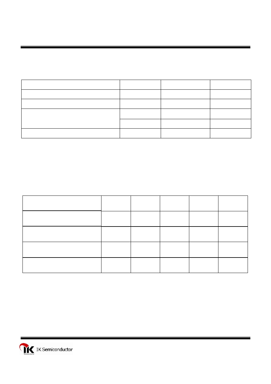
ABSOLUTE MAXIMUM RATINGS
(Unless otherwise stated, Ta=25
, GND=0V)
Parameter
Supply Voltage
Logic Input Voltage
Driver Output Current/Pin
Maximum Driver Output Current/Total
Symbol
V
DD
VI
ITOTAL
IOHSG
Rating
Units
-0.5 to +7.0
V
-0.5 to V
DD+
0.5
V
400
-50
mA
mA
+250
mA
IOLGR
RECOMMENDED OPERATING RANGE
(Unless otherwise stated, Ta= -20 to +70
, GND=0V)
Parameter
Logic Supply Voltage
Dynamic Current (see Note)
High-Level Input Voltage
Low-Level Input Voltage
Symbol
V
DD
I
DDdyn
V
IH
VIL
Min.
4.5
.
0.8V
DD
0
Typ.
5
.
.
.
Max.
Unit
5.5
V
5
mA
V
DD
V
0.3 V
DD
V
Note : Test Condition : Set Display Control Commands = 80H (Display Turn OFF State)

15
TECHNICAL DATA
LD1207
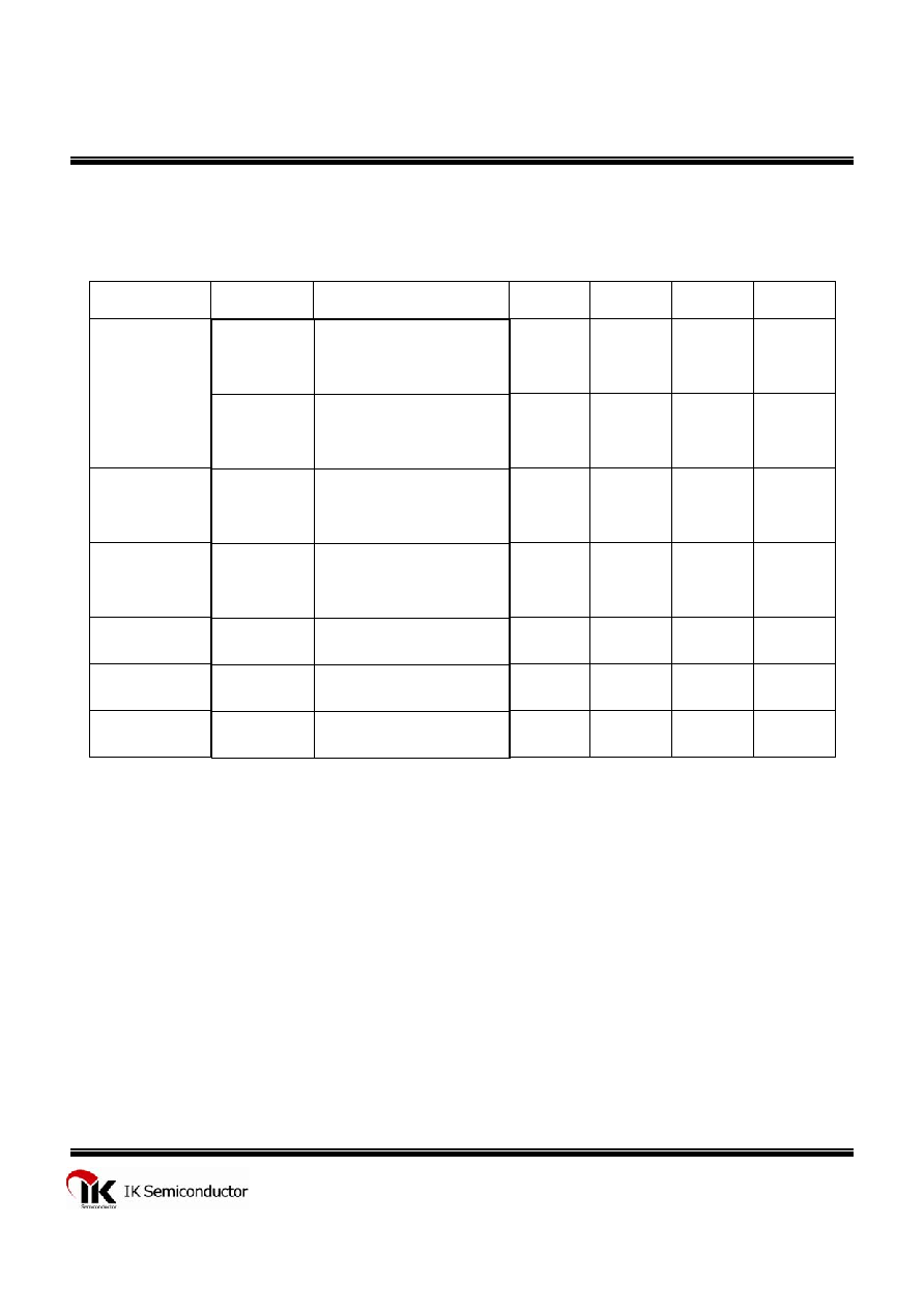
ELECTRICAL CHARACTERISTICS
(Unless otherwise stated, V
DD
=5V, GND=OV, Ta=25
,
Symbol
Test Condition
I
OHSG1
Min.
Typ.
Max.
Unit
Parameter
V
O
= V
DD
- 1V
SG1 to SG9.
SG10/GR7 to SG12/GR5
I
OHSG2
V
O
= V
DD
- 2V
SG1 to SG9.
SG10/GR 7 to SG12/GR5
-10
-14
-30
mA
High-Level
Output Current
I
OLGR
-20
-25
-50
mA
V
O
= 0.3V
GR1 TO GR4.
SG10/GR7 to SG12/GR5
I
TOLSG
Low-Level
Output Current
100
140
-
mA
V
O
= V
DD
- 1V
SG1 TO SG9.
SG10/GR7 to SG12/GR5
V
IH
Segment
High-Level
Output Current
Tolerance
-
-
±
5
%
-
V
IL
High-Level
Input Voltage
-
-
V
0.8VDD
Low-Level
Input Voltage
.
-
V
0.3VDD
-
Oscillation
Frequency
350
500
650
kHz
f
OSC
R = 51KOms

16
TECHNICAL DATA
LD1207
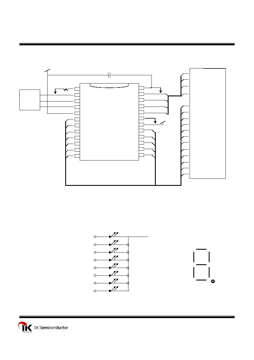
APPLICATION CIRCUIT
GND
VDD
SG12/GR5
SG11/GR6
SG10/GR7
SG9
SG8
GND
GR1
GR2
GR3
GR4
SG1
SG2
SG3
SG4
SG5
SG6
SG7
OSC
DIN
CLK
STB
VDD
S6
S7
S1
S2
S3
S4
S5
MCU
G1
G2
G3
G4
S9
S8
S12
S11
S10
G1
G2
G3
G4
S6
S7
S1
S2
S3
S4
S5
S8
S9
S10
S11
S12
SEG1
SEG2
SEG3
SEG4
SEG5
SEG6
SEG7
DIGIT1
DIGIT2
DIGIT3
DIGIT4
SEG8
SEG9
SEG10
SEG11
SEG12
4-GRID X 12-SEGMENT
(COMMON CAHODE)
+5V
+5V
51K
0.1pF
Note : The capacitor (0.1uF) connected between the GND and VDD Pins must be located as near as
possible to the LD1207 chip.
COMMON CATHODE TYPE LED PANEL
a
b
c
d
e
f
g
h
SEG1
COM/ DIGITAL(GRID)
a
SEG2
SEG3
b
f
g
SEG4
SEG5
c
e
SEG6
d
h
SEG7
SEG8

17
TECHNICAL DATA
LD1207
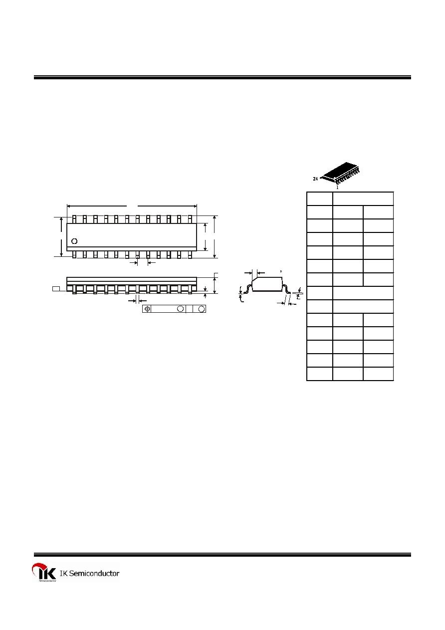
Package Dimensions(24SOP)
D SUFFIX SOIC
(MS - 013AD)
Symbol
MIN
MAX
A
15.20
15.60
B
7.40
7.60
C
2.35
2.65
D
0.33
0.51
F
0.40
1.27
G
H
NOTES:
J
0
∞
8
∞
1.
Dimensions A and B do not include mold flash or protrusion.
K
0.10
0.30
2.
Maximum mold flash or protrusion 0.15 mm (0.006) per side
M
0.23
0.32
for A; for B 0.25 mm (0.010) per side.
P
10.00
10.65
R
0.25
0.75
1.27
9.53
Dimension, mm
A
B
H
C
K
C M
J
F
M
P
G
D
R x 45
SEATING
PLANE
0.25 (0.010) M T
-T-
1
24
12
13

