 | –≠–ª–µ–∫—Ç—Ä–æ–Ω–Ω—ã–π –∫–æ–º–ø–æ–Ω–µ–Ω—Ç: 805L | –°–∫–∞—á–∞—Ç—å:  PDF PDF  ZIP ZIP |

Key Features
Applications
x
Embedded control systems
x
Battery≠operated systems
x
Intelligent instruments
x
Wireless communication systems
x
PDAs and handheld equipment
x
µ
P/
µ
C power supply monitoring
x
Design improvement over Maxim
MAX690A/692A/802L/802M/805L
-- 70% lower current than Maxim:
100
µ
A maximum
-- RESET Operation to 1.1V
x
Two precision supply-voltage monitor options
-- 4.65V (IMP690A/802L/805L)
-- 4.40V (IMP692A/802M)
x
Battery-backup power switch on-chip
x
Watchdog timer: 1.6 second timeout
x
Power failure/low battery detection
x
Short-circuit protection and thermal limiting
x
Small 8-pin SO package
x
No external components
x
Specified over full temperature range
Block Diagrams
+
≠
GND
Unregulated DC
Regulated +5V
V
OUT
V
CC
WDI
3.6V
Lithium
Battery
0.1
µ
F
PFO
V
BATT
PFI
R
1
R
2
RESET
RESET
V
CC
GND
GND
V
CC
CMOS
RAM
NMI
I/O LINE
BUS
690A_01.eps
IMP690A
IMP690A
IMP690A
, 692A
, 692A
, 802L/M, 805L
, 802L/M, 805L
P
OWER
M
ANAGEMENT
µ
µ
P P
P P
o
o
w
w
er Suppl
er Suppl
y Super
y Super
visor
visor
wit
wit
h Batt
h Batt
er
er
y Bac
y Bac
kup Switc
kup Switc
h
h
The IMP690A/IMP692A/IMP802L/IMP802M/IMP805L simplify power
supply monitoring and control in microprocessor systems. Each circuit
implements four functions: Reset control, watchdog monitoring, battery-
backup switching and power-failure monitoring. In addition to
microprocessor reset under powerup and power-down conditions, these
devices provide battery-backup switching to maintain control in power-
loss and brown-out situations. Additional monitoring capabilities
can provide an early warning of unregulated power-supply loss before
the voltage regulator drops out. The important features of these four
functions are:
a)
1.6 second watchdog timer to keep microprocessor responsive
b)
4.40V or 4.65V V
CC
threshold for microprocessor reset at power-up
and power-down
c)
SPDT (single-pole, double-throw) PMOS switch connects backup
power to RAM if V
CC
fails
d) 1.25V threshold detector for power loss or general purpose voltage
monitoring
While these features are pin≠compatible with the industry standard
power≠supply supervisors offered by Maxim, the IMP devices are supe-
rior replacements and can reduce power requirements by 70 percent
when compared to Maxim MAX690/MAX692A/MAX802L/MAX802M/
MAX805L devices. Short-circuit and thermal protection have also
been added.
The IMP690A/IMP802L/IMP805L generate a reset pulse when the
supply voltage drops below 4.65V, and the IMP692A/IMP802M
generate a reset below 4.40V. The IMP802L/IMP802M have power≠fail
accuracy to ±2%. The IMP805L is the same as the IMP690A except that
RESET is provided instead of
RESET.
IMP, Inc.
San Jose, CA
408-432-9100/www.impweb.com
+
+
+
+
+
+
+
+
V
CC
V
OUT
1
7
5
3
PFI
WDI
GND
V
BATT
8
2
6
4
PFO
IMP690A, IMP692A, IMP802L, IMP802M,
IMP805L
RESET
(RESET)
( ) IMP805L
Battery-Switchover
Circuit
Reset
Generator
Watchdog
Timer
3.5V
1.25V
1.25V
0.8V
690A_03.eps
Typical Application

Ordering Information
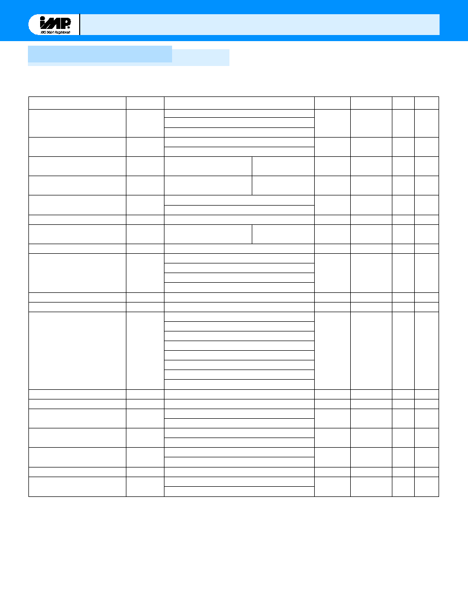
Pin Configuration
2
IMP690A
IMP690A
, 692A
, 692A
, 802L, 802M, 805L
, 802L, 802M, 805L
4
PFI
3
GND
2
V
CC
1
V
OUT
5
PFO
6
WDI
7
RESET (RESET)
8
V
BATT
690A_02.eps
IMP690A
IMP692A
IMP802L
IMP802M
IMP805L
( ) IMP805L
Plastic/CerDip/SO
Part Number
Reset Threshold (V)
Temperature Range
Pins-Package
IMP690A
IMP690ACPA
4.5 to 4.75
0
∞
C to +70
∞
C
8-Plastic DIP
IMP690ACSA
4.5 to 4.75
0
∞
C to +70
∞
C
8-SO
IMP690AC/D
4.5 to 4.75
25
∞
C
DICE
IMP690AEPA
≠ 40
∞
C to +85
∞
C
8-Plastic DIP
IMP690AESA
4.5 to 4.75
≠ 40
∞
C to +85
∞
C
8-SO
IMP690AMJA
4.5 to 4.75
Contact Factory
8-CerDIP
IMP692A
IMP692ACPA
4.25 to 4.50
0
∞
C to +70
∞
C
8-Plastic DIP
IMP692ACSA
4.25 to 4.50
0
∞
C to +70
∞
C
8-SO
IMP692AC/D
4.25 to 4.50
25
∞
C
DICE
IMP692AEPA
4.25 to 4.50
≠ 40
∞
C to +85
∞
C
8-Plastic DIP
IMP692AESA
4.25 to 4.50
≠ 40
∞
C to +85
∞
C
8-SO
IMP692AMJA
4.25 to 4.50
Contact Factory
8-CerDIP
IMP802L
IMP802LCPA
4.5 to 4.75
0
∞
C to +70
∞
C
8-Plastic DIP
IMP802LCSA
4.5 to 4.75
0
∞
C to +70
∞
C
8-SO
IMP802LEPA
4.5 to 4.75
≠ 40
∞
C to +85
∞
C
8-Plastic DIP
IMP802LESA
4.5 to 4.75
≠ 40
∞
C to +85
∞
C
8-SO
IMP802M
IMP802MCPA
4.25 to 4.50
0
∞
C to +70
∞
C
8-Plastic DIP
IMP802MCSA
4.25 to 4.50
0
∞
C to +70
∞
C
8-SO
IMP802MEPA
4.25 to 4.50
≠ 40
∞
C to +85
∞
C
8-Plastic DIP
IMP802MESA
4.25 to 4.50
≠ 40
∞
C to +85
∞
C
8-SO
IMP805L
IMP805LCPA
4.5 to 4.75
0
∞
C to +70
∞
C
8-Plastic DIP
IMP805LCSA
4.5 to 4.75
0
∞
C to +70
∞
C
8-SO
IMP805LC/D
4.5 to 4.75
25
∞
C
DICE
IMP805LEPA
4.5 to 4.75
≠40
∞
C to +85
∞
C
8-Plastic DIP
IMP805LESA
4.5 to 4.75
≠40
∞
C to +85
∞
C
8-SO
IMP805LMJA
4.5 to 4.75
Contact Factory
8-CerDIP

IMP690A
IMP690A
, 692A
, 692A
, 802L, 802M, 805L
, 802L, 802M, 805L
Absolute Maximum Ratings
Pin Description
Pin Terminal Voltage with Respect to Ground
V
CC
. . . . . . . . . . . . . . . . . . . . . . . . . . . . . . ≠0.3V to 6.0V
V
BATT
. . . . . . . . . . . . . . . . . . . . . . . . . . . . ≠0.3V to 6.0V
All Other Inputs* . . . . . . . . . . . . . . . . . . . ≠0.3V to (V
CC
+ 0.3V)
Input Current at V
CC
. . . . . . . . . . . . . . . . . . 200mA
Input Current at V
BATT
. . . . . . . . . . . . . . . . . 50mA
Input Current at GND . . . . . . . . . . . . . . . . . 20mA
Output Current:
V
OUT
. . . . . . . . . . . . . . . Short circuit protected
All Other Inputs . . . . . . . . . . . . . . . . . . . 20mA
Rate of Rise: V
BATT
and V
CC
. . . . . . . . . . 100V/
µ
s
Continuous Power Dissipation
Plastic DIP (derate 9mW/
∞
C above 70
∞
C) . . . 800mW
SO (derate 5.9mW/
∞
C above 70
∞
C) . . . . . . . . 500mW
CerDIP (derate 8mW/
∞
C above 70
∞
C) . . . . . . 650mW
Operating Temperature Range (C Devices) . . . . 0
∞
C to 70
∞
C
Operating Temperature Range (E Devices) . . . . ≠40
∞
C to 85
∞
C
Storage Temperature Range . . . . . . . . . . . . . . . . . ≠65
∞
C to 160
∞
C
Lead Temperature Soldering, (10 sec) . . . . . . . . 300
∞
C
* The input voltage limits on PFI and WDI may be exceeded if the
current is limited to less than 10mA
These are stress ratings only and functional operation is not implied.
Exposure to absolute maximum ratings for prolonged time periods may
affect device reliability.
Pin Number
IMP690A/IMP692A
IMP802L/IMP802M
IMP805L
Name
Function
1
1
V
OUT
Voltage supply for RAM. When V
CC
is above the reset threshold, V
OUT
connects to V
CC
through a P-channel MOS device. If V
CC
falls below the
reset threshold, this output will be connected to the backup supply at
V
BATT
(or V
CC
, whichever is higher) through the MOS switch to provide
continuous power to the CMOS RAM.
2
2
V
CC
+5V power supply input
3
3
GND
Ground
4
4
PFI
Power failure monitor input. PFI is connected to the internal power fail
comparator which is referenced to 1.25V. The power fail output (PFO)
is active LOW but remains HIGH if PFI is above 1.25V. If this feature is
unused, the PFI pin should be connected to GND or V
OUT
.
5
5
PFO
Power-fail output.
PFO is active LOW whenever the PFI pin is less than
1.25V.
6
6
WDI
Watchdog input. The WDI input monitors microprocessor activity. An
internal timer is reset with each transition of the WDI input. If WDI is held
HIGH or LOW for longer than the watchdog timeout period, typically 1.6
seconds, RESET (or
RESET) is asserted for the reset pulse width time,
t
RS
, of 140ms, minimum.
7
≠≠≠≠
RESET
Active-LOW reset output. When triggered by V
CC
falling below the reset
threshold or by watchdog timer timeout, RESET (or
RESET) pulses low
for the reset pulse width, t
RS
, typically 200ms. It will remain low if V
CC
is
below the reset threshold (4.65V in the IMP690A/IMP802L and 4.4V in
the IMP692A/IMP802L) and remains low for 200ms after V
CC
rise above
the reset threshold.
≠≠≠≠
7
RESET
Active-HIGH reset output. The inverse of
RESET.
8
8
V
BATT
Auxiliary power or backup-battery input. V
BATT
should be connected to
GND if the function is not used. This input has about 40mV of hysteresis
to prevent rapid toggling between V
CC
and V
BATT
.
3
4
IMP690A
IMP690A
, 692A
, 692A
, 802L, 802M, 805L
, 802L, 802M, 805L
Electrical Characteristics
Parameter
Symbol Conditions
Min
Typ
Max Units
V
CC
, V
BATT
Voltage Range
IMP69_AC, IMP802_C
1.1
5.5
V
(Note 1)
IMP805LC
1.1
5.5
IMP69_AE, IMP80_ _E
1.1
5.5
Supply Current Excluding I
OUT
I
S
IMP69_AC, IMP802_C
35
100
µ
A
IMP69_AE, IMP802_E, IMP805LE
35
100
I
SUPPLY
in Battery-Backup Mode
V
CC
= 0V, V
BATT
= 2.8V
T
A
= 25
∞
C
1.0
µ
A
(Excluding I
OUT
)
T
A
= T
MIN
to T
MAX
5.0
V
BATT
Standby Current
5.5V > V
CC
> V
BATT
≠ 0.2V
T
A
= 25
∞
C
≠ 0.1
0.02
µ
A
(Note 2)
T
A
= T
MIN
to T
MAX
≠1.0
0.02
V
OUT
Output
I
OUT
= 5mA
V
CC
≠ 0.025 V
CC
≠ 0.010
V
I
OUT
= 50mA
V
CC
≠ 0.25
V
CC
≠ 0.10
V
OUT
in Battery-Backup Mode
I
OUT
= 250
µ
A, V
CC
< V
BATT
≠ 0.2V
V
BATT
≠ 0.1 V
BATT
≠ 0.001
V
Battery Switch Threshold,
V
CC
< V
RT
Power-up
20
mV
V
CC
to V
BATT
Power-down
≠20
Battery Switchover Hysteresis
40
mV
Reset Threshold
V
RT
IMP690A/802L/805L
4.50
4.65
4.75
V
IMP692A, IMP802M
4.25
4.40
4.50
IMP802L, T
A
= 25∞C, V
CC
falling
4.55
4.70
IMP802M, T
A
= 25∞C, V
CC
falling
4.30
4.45
Reset Threshold Hysteresis
40
mV
Reset Pulse Width
t
RS
140
200
280
ms
Reset Output Voltage
I
SOURCE
= 800µA
V
CC
≠ 1.5
V
I
SINK
= 3.2mA
0.4
IMP69_AC, IMP802_C, V
CC
= 1.0V, I
SINK
= 50
µ
A
0.3
IMP69_AE, IMP802_E, V
CC
= 1.2V, I
SINK
= 100
µ
A
0.3
IMP805LC, I
SOURCE
= 4
µ
A, V
CC
= 1.1V
0.8
IMP805LE, I
SOURCE
= 4
µ
A, V
CC
= 1.2V
0.9
IMP805L, I
SOURCE
= 800
µ
A
V
CC
≠ 1.5
IMP805L, I
SINK
= 3.2mA
0.4
Watchdog Timeout
t
WD
1.00
1.60
2.25
sec
WDI Pulse Width
t
WP
V
IL
= 0.4V, V
IH
= 0.8V
CC
50
ns
WDI Input Current
WDI = V
CC
50
150
µ
A
WDI = 0V
≠150
≠50
WDI Input Threshold
V
CC
= 5V, Logic LOW
0.8
V
(Note 3)
V
CC
= 5V, Logic HIGH
3.5
PFI Input Threshold
IMP69_A, IMP805L, V
CC
= 5V
1.20
1.25
1.30
V
IMP802_C/E, V
CC
= 5V
1.225
1.250
1.275
PFI Input Current
≠ 25
0.01
25
nA
PFO Output Voltage
I
SOURCE
= 800µA
V
CC
≠ 1.5
V
I
SINK
= 3.2mA
0.4
Unless otherwise noted V
CC
= 4.75V to 5.5V for the IMP690A/IMP802L/IMP805L and V
CC
= 4.5V to 5.5V for the IMP692A/IMP802M;
V
BATT
= 2.8V; and T
A
= T
MIN
to T
MAX
.
Notes: 1. If V
CC
or V
BATT
is 0V, the other must be greater than 2.0V.
2. Battery charging-current is "≠". Battery discharge-current is "+".
3. WDI is guaranteed to be in an intermediate level state if WDI is floating and V
CC
is within the operating voltage range. WDI input
impedance is 50k
. WDI is biased to 0.3V
CC
.
5
IMP690A
IMP690A
, 692A
, 692A
, 802L, 802M, 805L
, 802L, 802M, 805L
Application Information
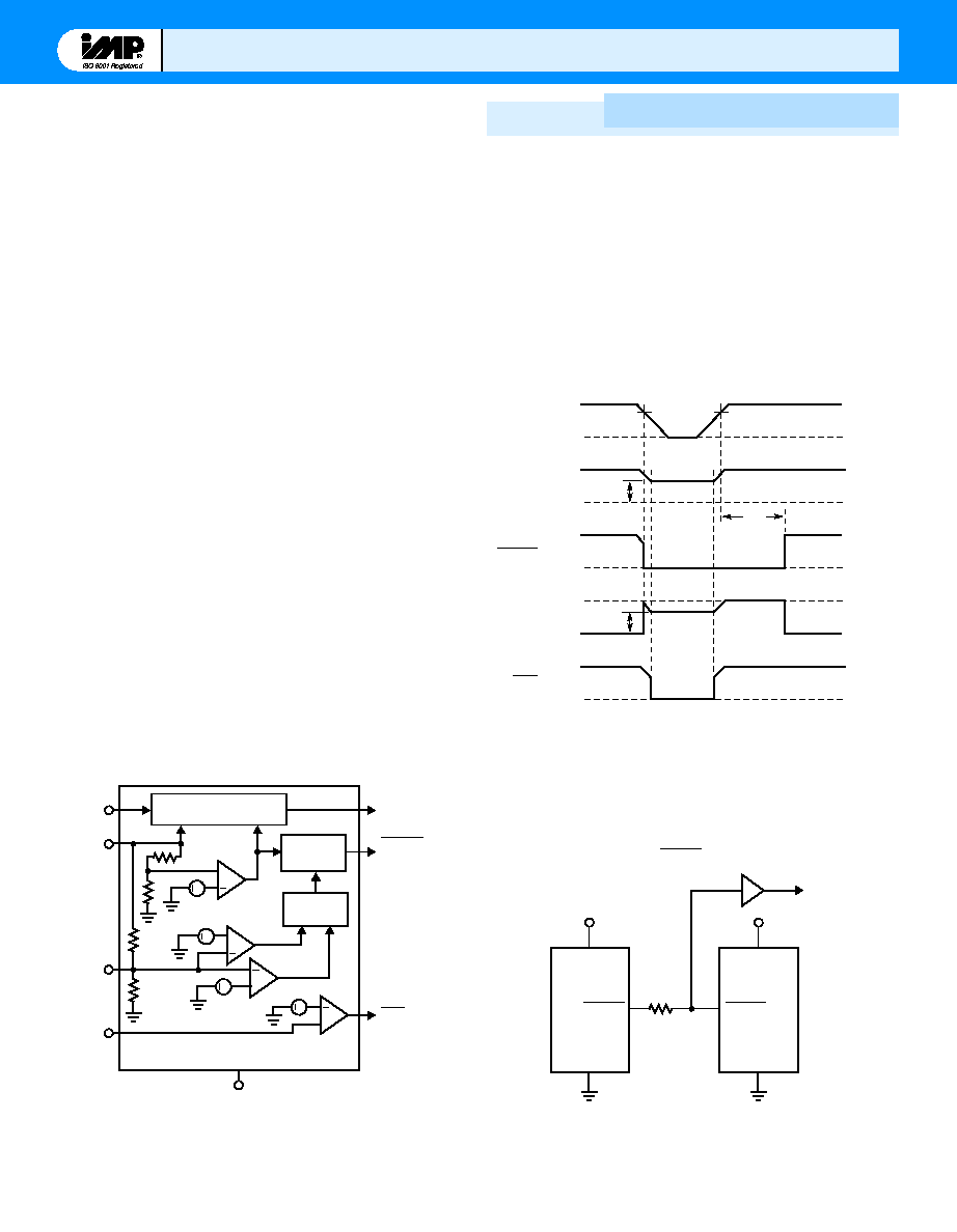
Reset Output
It is important to initialize a microprocessor to a known state in
response to specific events that could create code execution errors
and "lock-up". The reset output of these supervisory circuits send
a reset pulse to the microprocessor in response to power-up,
power-down/power-loss or a watchdog time-out. The reset pulse
width, t
RS
, is typically around 200ms and is LOW for the
IMP690A, IMP692A, IMP802 and HIGH for the IMP805L.
Power-up reset occurs when a rising V
CC
reaches the reset thresh-
old, V
RT
, forcing a reset condition in which the reset output is
asserted in the appropriate logic state for the duration of t
RS
.
Figure 2 shows the reset pin timing.
Power-loss or "brown-out" reset occurs when V
CC
dips below the
reset threshold resulting in a reset assertion for the duration of t
RS
.
The reset signal remains asserted as long as V
CC
is between V
RT
and 1.1V, the lowest V
CC
for which these devices can provide a
guaranteed logic-low output. To ensure logic inputs connected to
the IMP690A/692A/802 RESET pin are in a known state when
V
CC
is under 1.1V, a 100k
pull-down resistor at RESET is needed:
the logic-high IMP805L will need a pull-up resistor to V
CC
.
A Watchdog time-out reset occurs when a logic "1" or logic "0" is
continuously applied to the WDI pin for more than 1.6 seconds.
After the duration of the reset interval, the watchdog timer starts
a new 1.6 second timing interval; the microprocessor must service
the watchdog input by changing states or by floating the WDI pin
before this interval is finished. If the WDI pin is held either HIGH
or LOW, a reset pulse will be triggered every 1.8 seconds (the 1.6
second timing interval plus the reset pulse width t
RS
).
Microprocessor Interface.
The IMP690 has logic-LOW RESET output while the IMP805 has
an inverted logic-HIGH RESET output. Microprocessors with bi-
directional reset pins (69HC11 for example) can pose a problem
when the supervisory circuit and the microprocessor output pins
attempt to go to opposite logic states. The problem can be
resolved by placing a 4.7k
resistor between the RESET output
and the microprocessor reset pin. This is shown in Figure 3. Since
the series resistor limits drive capabilities, the reset signal to other
devices should be buffered.
+
+
+
+
+
+
+
+
V
CC
V
OUT
1
7
5
3
PFI
WDI
GND
V
BATT
8
2
6
4
PFO
IMP690A, IMP692A, IMP802L, IMP802M,
IMP805L
RESET
(RESET)
( ) IMP805L
Battery-Switchover
Circuit
Reset
Generator
Watchdog
Timer
3.5V
1.25V
1.25V
0.8V
690A_03.eps
Figure 1. Block Diagram
V
CC
V
OUT
V
BATT
= PFI = 3.0V
I
OUT
= 0mA
PFO
+ 5V
+ 5V
+ 0V
+ 0V
3.0V
+ 5V
+ 0V
+ 5V
+ 0V
+ 5V
+ 0V
( ) IMP805L
3.0V
RESET
(RESET)
690A_04.eps
t
RS
Figure 2. Timing Diagram
690A_05.eps
GND
GND
RESET
RESET
V
CC
IMP690A
V
CC
4.7k
Buffered RESET to Other System Components
Figure 3. Interfacing with bi-directional microprocessor
reset inputs