87
© IMP, Inc.
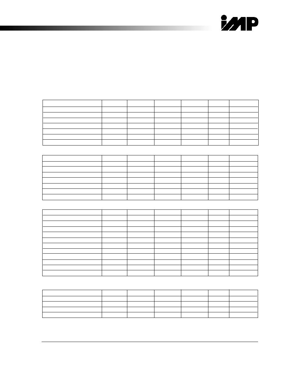
Process C3014
CMOS 3
µ
m
5 Volt Single Metal Analog
Electrical Characteristics
T=25
o
C Unless otherwise noted
ISO 9001 Registered
Æ
N-Channel Transistor
Symbol
Minimum
Typical
Maximum
Unit
Comments
Threshold Voltage
VT
N
0.5
0.65
0.8
V
100x3
µ
m
Body Factor
N
0.6
V
1/2
100x3
µ
m
Conduction Factor
N
42
47
52
µ
A/V
2
100x100
µ
m
Effective Channel Length
Leff
N
2.0
2.3
2.6
µ
m
100x3
µ
m
Width Encroachment
W
N
0.7
µ
m
Per side
Punch Through Voltage
BVDSS
N
12
V
Poly Field Threshold Voltage
VTF
P(N)
12
V
P-Channel Transistor
Symbol
Minimum
Typical
Maximum
Unit
Comments
Threshold Voltage
VT
P
≠0.5
0.65
≠0.8
V
100x3
µ
m
Body Factor
P
0.55
V
1/2
100x3
µ
m
Conduction Factor
P
13
15
19
µ
A/V
2
100x100
µ
m
Effective Channel Length
Leff
P
2.85
3.2
3.55
µ
m
100x3
µ
m
Width Encroachment
W
P
0.9
µ
m
Per side
Punch Through Voltage
BVDSS
P
≠12
V
Poly Field Threshold Voltage
VTF
P(P)
≠12
V
Diffusion & Thin Films
Symbol
Minimum
Typical
Maximum
Unit
Comments
Well (field) Sheet Resistance
P-well(f)
3.2
4.8
6.5
K
/
P-well
N+ Sheet Resistance
N+
16
21
27
/
N+ Junction Depth
x
jN+
0.8
µ
m
P+ Sheet Resistance
P+
50
80
100
/
P+ Junction Depth
x
jP+
0.7
µ
m
Gate Oxide Thickness
T
GOX
44
48
52
nm
Interpoly Oxide Thickness
T
P1P2
60 nm
Gate Poly Sheet Resistance
POLY1
15
22
30
/
Bottom Poly Sheet Res.
POLY2
20
30
40
/
Metal-1 Sheet Resistance
M1
30
60
m
/
Passivation Thickness
T
PASS
200+900 nm
oxide+nit.
Capacitance
Symbol
Minimum
Typical
Maximum
Unit
Comments
Gate Oxide
C
OX
0.66
0.72
0.78
fF/
µ
m
2
Metal-1 to Poly-1
C
M1P
0.0523
fF/
µ
m
2
Metal-1 to Silicon
C
M1S
0.026
0.030
0.034
fF/
µ
m
2
Poly-1 to Poly-2
C
P1P2
0.51
0.57
0.63
fF/
µ
m
2

88
C3014-4-98
Process C3014
Physical Characteristics
Starting Material
N <100>
N+/P+ Width/Space
3.0 / 3.0
µ
m
Starting Mat. Resistivity
15 - 25
-cm
N+ To P+ Space
12
µ
m
Typ. Operating Voltage
5V
Contact To Poly Space
2.5
µ
m
Well Type
P-well
Contact Overlap Of Diffusion
1.5
µ
m
Metal Layers
1
Contact Overlap Of Poly
1.0
µ
m
Poly Layers
2
Metal-1 Overlap Of Contact
1.0
µ
m
Contact Size
2.0x2.0
µ
m
Minimum Pad Opening
100x100
µ
m
Metal-1 Width/Space
3.5 / 2.5
µ
m
Minimum Pad-to-Pad Spacing
55
µ
m
Gate Poly Width/Space
4.0 / 2.5
µ
m
Minimum Pad Pitch
80.0
µ
m
Special Feature of C3014 Process: P-well analog low threshold process with single metal
CMOS 3.0
µ
m technology for 5 Volt applications.