 | –≠–ª–µ–∫—Ç—Ä–æ–Ω–Ω—ã–π –∫–æ–º–ø–æ–Ω–µ–Ω—Ç: IMP1811-X | –°–∫–∞—á–∞—Ç—å:  PDF PDF  ZIP ZIP |
Document Outline
- Cover
- Cross Reference
- IMP1810
- IMP1811
- IMP1812
- IMP1815
- IMP1816
- IMP1817
- IMP1233D
- IMP1233M
- Package Information

Supervisors
POWER
MANAGEMENT
408-432-9100/www.impweb.com
IMP1
IMP1
8
8
1
1
0 -- Lo
0 -- Lo
w P
w P
o
o
w
w
er
er
, 5V
, 5V
µ
µ
P R
P R
eset
eset
Active LOW, Push-Pull Output
IMP1
IMP1
8
8
1
1
1 -- Lo
1 -- Lo
w P
w P
o
o
w
w
er
er
, 5V
, 5V
µ
µ
P R
P R
eset
eset
Active LOW, Open-Drain Output
IMP1
IMP1
8
8
1
1
2 -- Lo
2 -- Lo
w P
w P
o
o
w
w
er
er
, 5V
, 5V
µ
µ
P R
P R
eset
eset
Active HIGH, Push-Pull Output
IMP1
IMP1
8
8
1
1
5 -- Lo
5 -- Lo
w P
w P
o
o
w
w
er
er
, 3.3V/3.0V
, 3.3V/3.0V
µ
µ
P R
P R
eset
eset
Active LOW, Push-Pull Output
IMP1
IMP1
8
8
1
1
6 -- Lo
6 -- Lo
w P
w P
o
o
w
w
er
er
, 3.3V/3.0V
, 3.3V/3.0V
µ
µ
P R
P R
eset
eset
Active LOW, Open-Drain Output
IMP1
IMP1
8
8
1
1
7 -- Lo
7 -- Lo
w P
w P
o
o
w
w
er
er
, 3.3V/3.0V
, 3.3V/3.0V
µ
µ
P R
P R
eset
eset
Active HIGH, Push-Pull Output
IMP1
IMP1
233D -- Lo
233D -- Lo
w P
w P
o
o
w
w
er
er
, 5V
, 5V
µ
µ
P R
P R
eset
eset
Active LOW, Open-Drain Output
IMP1
IMP1
233M -- Lo
233M -- Lo
w P
w P
o
o
w
w
er
er
, 5V/3.0V
, 5V/3.0V
µ
µ
P R
P R
eset
eset
Active LOW, Open-Drain Output
The part numbers and descriptions are linked to the data sheet.
408-432-9100/www.impweb.com
©
1999 IMP, Inc.
µ
P Supervisor Products: Low Power Alternatives to Dallas Semiconductor
g
n
i
r
e
d
r
O
P
M
I
r
e
b
m
u
N
t
r
a
P
T
E
S
E
R
)
V
(
e
g
a
tl
o
V
T
E
S
E
R
)
%
(
e
c
n
a
r
e
l
o
T
e
m
i
T
T
E
S
E
R
)
s
m
(
T
E
S
E
R
y
ti
r
a
l
o
P
ll
u
P
-
h
s
u
P
e
g
a
t
S
t
u
p
t
u
O
n
i
a
r
D
n
e
p
O
t
u
p
t
u
O
O
S
n
i
P
-
8
e
g
a
k
c
a
P
2
9
-
O
T
e
g
a
k
c
a
P
3
2
-
T
O
S
e
g
a
k
c
a
P
3
2
2
-
T
O
S
e
g
a
k
c
a
P
5
-
0
1
8
1
P
M
I
0
2
6
.
4
5
0
5
1
W
O
L
X
X
0
1
-
0
1
8
1
P
M
I
0
7
3
.
4
0
1
0
5
1
W
O
L
X
X
5
1
-
0
1
8
1
P
M
I
0
2
1
.
4
5
1
0
5
1
W
O
L
X
X
5
-
R
0
1
8
1
P
M
I
0
2
6
.
4
5
0
5
1
W
O
L
X
X
0
1
-
R
0
1
8
1
P
M
I
0
7
3
.
4
0
1
0
5
1
W
O
L
X
X
5
1
-
R
0
1
8
1
P
M
I
0
2
1
.
4
5
1
0
5
1
W
O
L
X
X
5
-
1
1
8
1
P
M
I
0
2
6
.
4
5
0
5
1
W
O
L
X
X
0
1
-
1
1
8
1
P
M
I
0
5
3
.
4
0
1
0
5
1
W
O
L
X
X
5
1
-
1
1
8
1
P
M
I
0
3
1
.
4
5
1
0
5
1
W
O
L
X
X
5
-
R
1
1
8
1
P
M
I
0
2
6
.
4
5
0
5
1
W
O
L
X
X
0
1
-
R
1
1
8
1
P
M
I
0
5
3
.
4
0
1
0
5
1
W
O
L
X
X
5
1
-
R
1
1
8
1
P
M
I
0
3
1
.
4
5
1
0
5
1
W
O
L
X
X
5
-
2
1
8
1
P
M
I
0
2
6
.
4
5
0
5
1
H
G
I
H
X
X
0
1
-
2
1
8
1
P
M
I
0
5
3
.
4
0
1
0
5
1
H
G
I
H
X
X
5
1
-
2
1
8
1
P
M
I
0
3
1
.
4
5
1
0
5
1
H
G
I
H
X
X
5
-
R
2
1
8
1
P
M
I
0
2
6
.
4
5
0
5
1
H
G
I
H
X
X
0
1
-
R
2
1
8
1
P
M
I
0
5
3
.
4
0
1
0
5
1
H
G
I
H
X
X
5
1
-
R
2
1
8
1
P
M
I
0
3
1
.
4
5
1
0
5
1
H
G
I
H
X
X
5
-
5
1
8
1
P
M
I
0
6
0
.
3
5
0
5
1
W
O
L
X
X
0
1
-
5
1
8
1
P
M
I
0
8
8
.
2
0
1
0
5
1
W
O
L
X
X
0
2
-
5
1
8
1
P
M
I
0
5
5
.
2
0
2
0
5
1
W
O
L
X
X
5
-
R
5
1
8
1
P
M
I
0
6
0
.
3
5
0
5
1
W
O
L
X
X
0
1
-
R
5
1
8
1
P
M
I
0
8
8
.
2
0
1
0
5
1
W
O
L
X
X
0
2
-
R
5
1
8
1
P
M
I
0
5
5
.
2
0
2
0
5
1
W
O
L
X
X
5
-
6
1
8
1
P
M
I
0
6
0
.
3
5
0
5
1
W
O
L
X
X
0
1
-
6
1
8
1
P
M
I
0
8
8
.
2
0
1
0
5
1
W
O
L
X
X
0
2
-
6
1
8
1
P
M
I
0
5
5
.
2
0
2
0
5
1
W
O
L
X
X
5
-
R
6
1
8
1
P
M
I
0
6
0
.
3
5
0
5
1
W
O
L
X
X
0
1
-
R
6
1
8
1
P
M
I
0
8
8
.
2
0
1
0
5
1
W
O
L
X
X
0
2
-
R
6
1
8
1
P
M
I
0
5
5
.
2
0
2
0
5
1
W
O
L
X
X
5
-
7
1
8
1
P
M
I
0
6
0
.
3
5
0
5
1
H
G
I
H
X
X
0
1
-
7
1
8
1
P
M
I
0
8
8
.
2
0
1
0
5
1
H
G
I
H
X
X
0
2
-
7
1
8
1
P
M
I
0
5
5
.
2
0
2
0
5
1
H
G
I
H
X
X
5
-
R
7
1
8
1
P
M
I
0
6
0
.
3
5
0
5
1
H
G
I
H
X
X
0
1
-
R
7
1
8
1
P
M
I
0
8
8
.
2
0
1
0
5
1
H
G
I
H
X
X
0
2
-
R
7
1
8
1
P
M
I
0
5
5
.
2
0
2
0
5
1
H
G
I
H
X
X
5
-
D
3
3
2
1
P
M
I
5
2
6
.
4
5
0
5
3
W
O
L
X
X
0
1
-
D
3
3
2
1
P
M
I
5
7
3
.
4
0
1
0
5
3
W
O
L
X
X
5
1
-
D
3
3
2
1
P
M
I
5
2
1
.
4
5
1
0
5
3
W
O
L
X
X
5
-
Z
D
3
3
2
1
P
M
I
5
2
6
.
4
5
0
5
3
W
O
L
X
X
0
1
-
Z
D
3
3
2
1
P
M
I
5
7
3
.
4
0
1
0
5
3
W
O
L
X
X
5
1
-
Z
D
3
3
2
1
P
M
I
5
2
1
.
4
5
1
0
5
3
W
O
L
X
X
5
5
-
M
3
3
2
1
P
M
I
5
2
6
.
4
5
0
5
3
W
O
L
X
X
5
-
M
3
3
2
1
P
M
I
5
7
3
.
4
0
1
0
5
3
W
O
L
X
X
3
-
M
3
3
2
1
P
M
I
0
2
7
.
2
5
1
0
5
3
W
O
L
X
X
5
5
-
S
M
3
3
2
1
P
M
I
5
2
6
.
4
5
0
5
3
W
O
L
X
X
5
-
S
M
3
3
2
1
P
M
I
5
7
3
.
4
0
1
0
5
3
W
O
L
X
X
3
-
S
M
3
3
2
1
P
M
I
0
2
7
.
2
5
1
0
5
3
W
O
L
X
X
7
0
t
_
B
/
D
L
E
µ
µ
P Super
P Super
visor Cr
visor Cr
oss R
oss R
ef
ef
er
er
ence
ence

©
1999 IMP, Inc.
408-432-9100/www.impweb.com
1
Key Features
Applications
x
Set-top boxes
x
Cellular phones
x
PDAs
x
Energy management systems
x
Embedded control systems
x
Printers
x
Single board computers
x
Improved Dallas DS1810 replacement
-- 50% lower maximum supply current
x
Low Supply Current
-- 20µA maximum (5.5V)
x
Automatically restarts a microprocessor after
power failure
x
150ms reset delay after V
CC
returns to an
in-tolerance condition
x
Active LOW power-up reset
x
Precision temperature-compensated voltage
reference and comparator
x
Eliminates external components
x
Low-cost TO-92 package
x
Compact surface mount SOT-23 package
x
Push-Pull output for minimum current drain
x
Operating temperature ≠40
∞
C to +85
∞
C
Block Diagram
≠
+
1810_01.eps
V
CC
1
RESET
GND
3
2
Supply
Tolerance
Bias
IMP1810
Delay
150ms Typical
Reference
IMP1
IMP1
8
8
1
1
0
0
P
OWER
M
ANAGEMENT
Lo
Lo
w P
w P
o
o
w
w
er
er
, 5V
, 5V
µ
µ
P R
P R
eset
eset
≠ A
≠ A
ctiv
ctiv
e L
e L
O
O
W
W
, Push-Pull Output
, Push-Pull Output
The IMP1810 supply voltage monitor is an improved, low-power
replacement for the Dallas Semiconductor DS1810. Maximum supply
current over temperature is a low 20
µ
A, representing 50 percent lower
power as compared to the DS1810.
The IMP1810 issues an active LOW reset signal whenever the monitored
supply is out-of-tolerance. A precision reference and comparator circuit
monitor power supply (V
CC
) level. Tolerance level options are 5-, 10- and
15-percent. When an out-of-tolerance condition is detected, an internal
power-fail signal is generated which forces an active LOW reset signal.
After V
CC
returns to an in-tolerance condition, the reset signal remains
active for 150ms to allow the power supply and system microprocessor
to stabilize.
The IMP1810 is designed with a push-pull output stage and operates
over the extended industrial temperature range. Devices are available in
compact surface mount SOT-23 packages and 3-lead TO-92 packages.
Other low power products in this family include the IMP1811/12/15/16/17,
IMP1233D and IMP1233M.
Typical Application
IMP1810
Microprocessor
RESET
RESET
1810_02.eps
VCC
GND
t
r
a
P
e
g
a
t
l
o
V
T
E
S
E
R
)
V
(
e
m
i
T
T
E
S
E
R
)
s
m
(
t
u
p
t
u
O
e
g
a
t
S
T
E
S
E
R
y
t
i
r
a
l
o
P
0
1
8
1
P
M
I
0
2
1
.
4
,
0
7
3
.
4
,
0
2
6
.
4
0
5
1
ll
u
P
-
h
s
u
P
W
O
L
1
1
8
1
P
M
I
0
3
1
.
4
,
0
5
3
.
4
,
0
2
6
.
4
0
5
1
n
i
a
r
D
-
n
e
p
O
W
O
L
2
1
8
1
P
M
I
0
3
1
.
4
,
0
5
3
.
4
,
0
2
6
.
4
0
5
1
ll
u
P
-
h
s
u
P
H
G
I
H
5
1
8
1
P
M
I
0
5
5
.
2
,
0
8
8
.
2
,
0
6
0
.
3
0
5
1
ll
u
P
-
h
s
u
P
W
O
L
6
1
8
1
P
M
I
0
5
5
.
2
,
0
8
8
.
2
,
0
6
0
.
3
0
5
1
n
i
a
r
D
-
n
e
p
O
W
O
L
7
1
8
1
P
M
I
0
5
5
.
2
,
0
8
8
.
2
,
0
6
0
.
3
0
5
1
ll
u
P
-
h
s
u
P
H
G
I
H
D
3
3
2
1
P
M
I
5
2
1
.
4
,
5
7
3
.
4
,
5
2
6
.
4
0
5
3
n
i
a
r
D
-
n
e
p
O
W
O
L
M
3
3
2
1
P
M
I
0
2
7
.
2
,
5
7
3
.
4
,
5
2
6
.
4
0
5
3
n
i
a
r
D
-
n
e
p
O
W
O
L
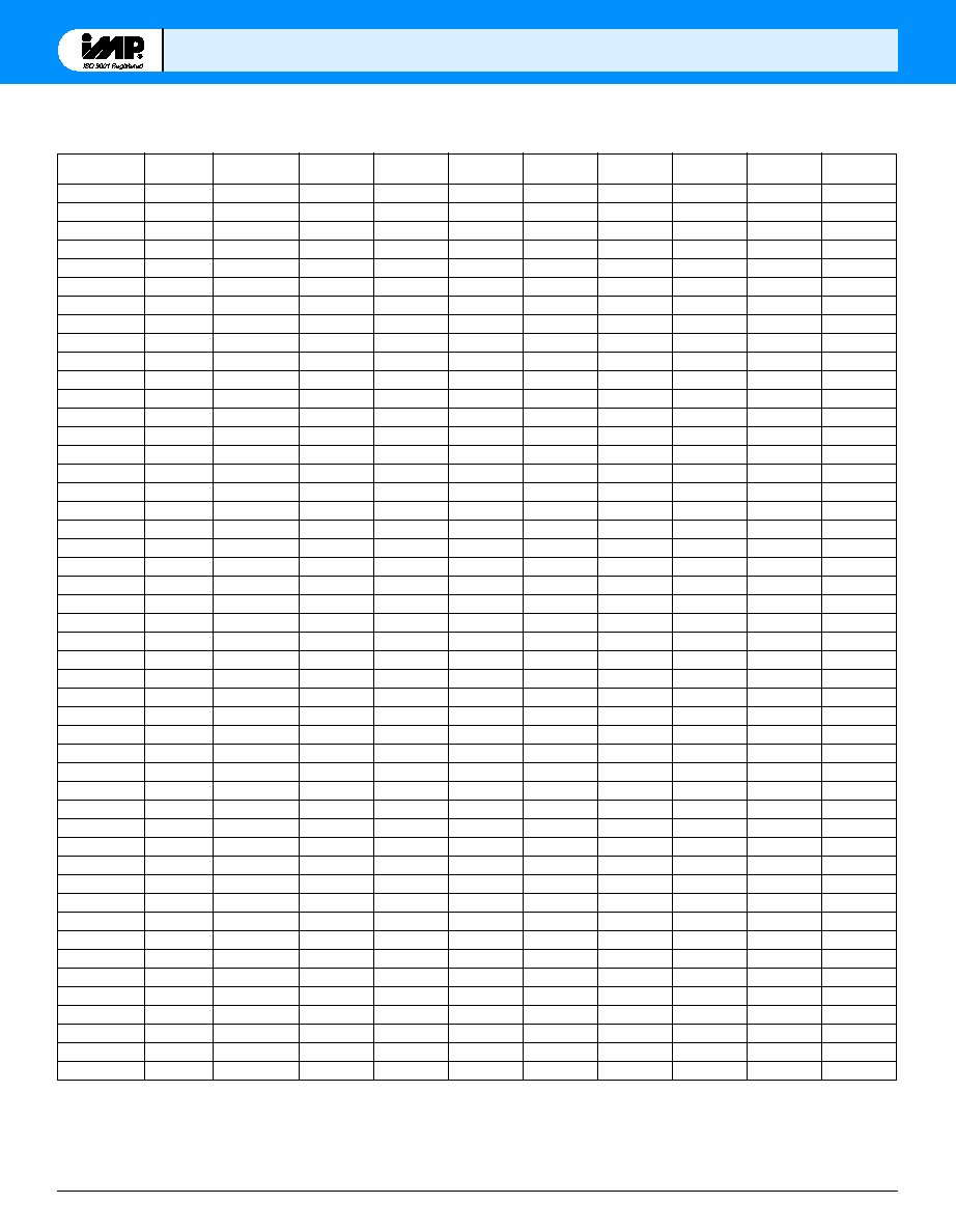
Family Selection Guide
2
408-432-9100/www.impweb.com
©
1999 IMP, Inc.
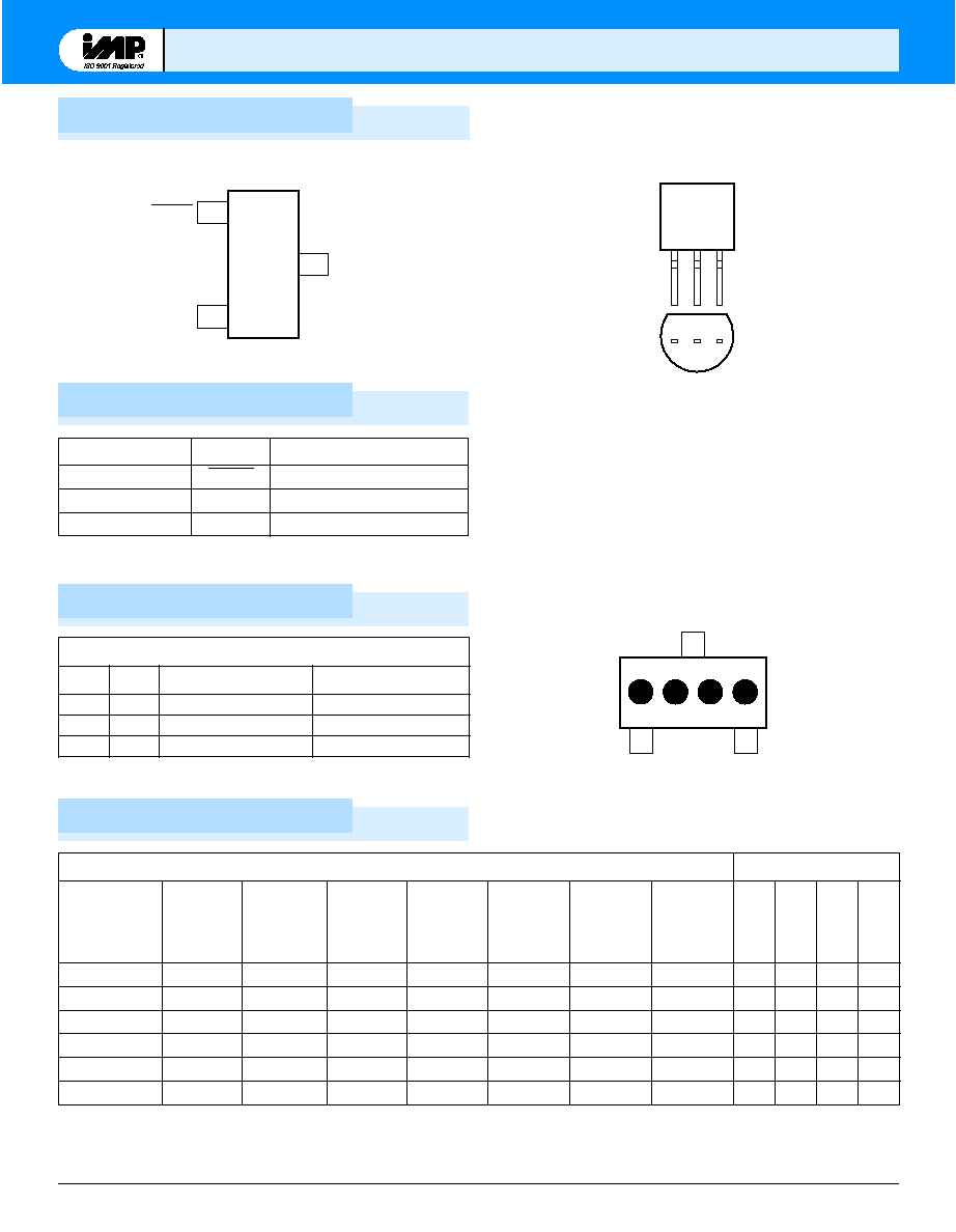
Pin Configuration
IMP1
IMP1
8
8
1
1
0
0
Pin Descriptions
Pin Number
Name
Function
1
RESET
Active LOW reset output
2
V
CC
Power supply input
3
GND
Ground
IMP1810-X
RESET
V
CC
GND
3
1
2
1810_03.eps
Package Marking Code
Ordering Information
1810_04.eps
1
2
3
IMP1810-X
SOT23
TO-92*
1810_05a.eps
3
1
2
A
B
C
D
3
2
-
T
O
S
e
d
o
C
r
e
t
t
e
L
e
g
a
k
c
a
P
A
B
t
r
a
P
e
c
n
a
r
e
l
o
T
t
e
s
e
R
B
A
0
1
8
1
P
M
I
%
5
B
B
0
1
8
1
P
M
I
%
0
1
B
C
0
1
8
1
P
M
I
%
5
1
s
p
e
.
2
0
t
_
0
1
8
1
*
Add /S to Part Number for straight (unformed) leads. (ie. IMP18xx-x/S)
XX = Date code
**
Add /T to Part Number for Tape and Reel. (ie. IMP18xx-x/T)
y
r
a
m
m
u
S
e
c
i
v
e
D
g
n
i
k
r
a
M
e
g
a
k
c
a
P
*
*
t
r
a
P
r
e
b
m
u
N
T
E
S
E
R
t
u
p
t
u
O
e
g
a
t
l
o
V
)
V
(
T
E
S
E
R
e
c
n
a
r
e
l
o
T
)
%
(
T
E
S
E
R
e
m
i
T
)
s
m
(
ll
u
P
-
h
s
u
P
t
u
p
t
u
O
e
g
a
t
S
*
2
9
-
O
T
e
g
a
k
c
a
P
3
2
-
T
O
S
e
g
a
k
c
a
P
T
E
S
E
R
y
t
i
r
a
l
o
P
A
B
C
D
5
-
0
1
8
1
P
M
I
2
6
.
4
5
0
5
1
W
O
L
0
1
-
0
1
8
1
P
M
I
7
3
.
4
0
1
0
5
1
W
O
L
5
1
-
0
1
8
1
P
M
I
2
1
.
4
5
1
0
5
1
W
O
L
5
-
R
0
1
8
1
P
M
I
2
6
.
4
5
0
5
1
W
O
L
B
A
X
X
0
1
-
R
0
1
8
1
P
M
I
7
3
.
4
0
1
0
5
1
W
O
L
B
B
X
X
5
1
-
R
0
1
8
1
P
M
I
2
1
.
4
5
1
0
5
1
W
O
L
B
C
X
X

©
1999 IMP, Inc.
408-432-9100/www.impweb.com
3
IMP1
IMP1
8
8
1
1
0
0
Absolute Maximum Ratings
Electrical Characteristics
Voltage on V
CC
. . . . . . . . . . . . . . . . . . . . . . . . ≠0.5V to 7V
Voltage on RESET . . . . . . . . . . . . . . . . . . . . . ≠0.5V to V
CC
+ 0.5V
Operating Temperature Range . . . . . . . . . . . ≠40
∞
C to 85
∞
C
Soldering Temperature . . . . . . . . . . . . . . . . . . 260
∞
C for 10 seconds
Storage Temperature . . . . . . . . . . . . . . . . . . . ≠55
∞
C to 125
∞
C
Voltages measured with respect to ground.
These are stress ratings only and functional operation is not implied.
Parameter
Symbol
Conditions
Min
Typ
Max
Units
Supply Voltage
V
CC
1.2
5.5
V
Output Voltage
V
OH
I
OUT
< 500
µ
A
V
CC
≠ 0.5V
V
CC
≠ 0.1V
V
Output Current
I
OH
Output = 2.4V, V
CC
2.7V
350
µ
A
Output Current
I
OL
Output = 0.4V, V
CC
2.7V
+10
mA
Operating Current
I
CC
V
CC
< 5.5V, RESET output open
8
20
µ
A
V
CC
Trip Point (IMP1810-5)
V
CCTP
4.50
4.62
4.75
V
V
CC
Trip Point (IMP1810-10)
V
CCTP
4.25
4.37
4.49
V
V
CC
Trip Point (IMP1810-15)
V
CCTP
4.00
4.12
4.24
V
Output Capacitance
C
OUT
10
pF
V
CC
Detect to RESET Low
t
RPD
2
5
µ
s
V
CC
Slew Rate
t
F
300
µ
s
(V
CCTP
(MAX) to V
CCTP
(MIN))
V
CC
Slew Rate
t
R
0
ns
(V
CCTP
(MIN) to V
CCTP
(MAX))
V
CC
Detect to RESET High
t
RPU
t
r
= 5
µ
s
100
150
300
ms
Unless otherwise noted, V
CC
= 1.2V to 5.5V and specifications are over the operating temperature range of ≠ 40
∞
C to +85
∞
C.
All voltages are referenced to ground.
Notes 1. The t
F
value is for reference in defining values for t
RPD
and should not be considered a requirement for proper operation or use.