 | –≠–ª–µ–∫—Ç—Ä–æ–Ω–Ω—ã–π –∫–æ–º–ø–æ–Ω–µ–Ω—Ç: IMP2014 | –°–∫–∞—á–∞—Ç—å:  PDF PDF  ZIP ZIP |
Document Outline
- Front Cover
- LDO Selection Guide
- IMP37
- IMP2014/15, IMP2185
- IMP2054/55, IMP2186
- IMP2070/71, IMP2187
- Package Dimensions

LDOs
POWER
MANAGEMENT
408-432-9100/www.impweb.com
IMP3
IMP3
7 -- Lo
7 -- Lo
w Dr
w Dr
opout P
opout P
ositiv
ositiv
e V
e V
olt
olt
ag
ag
e R
e R
egulat
egulat
or
or
With 800mA Output
IMP20
IMP20
1
1
4/1
4/1
5, IMP2
5, IMP2
1
1
85 -- Super Lo
85 -- Super Lo
w Dr
w Dr
opout CMOS R
opout CMOS R
egulat
egulat
or
or
s
s
With Battery Life Extending Shutdown Mode
IMP205
IMP205
4/55, IMP2
4/55, IMP2
1
1
86 -- Super Lo
86 -- Super Lo
w Dr
w Dr
opout CMOS R
opout CMOS R
egulat
egulat
or
or
s
s
With Battery Life Extending Shutdown Mode and ERROR Output
IMP20
IMP20
70/7
70/7
1
1
, IMP2
, IMP2
1
1
8
8
7 -- Super Lo
7 -- Super Lo
w Dr
w Dr
opout CMOS R
opout CMOS R
egulat
egulat
or
or
s
s
With Battery Life Extending Shutdown Mode and Adjustable Output
Each Part Number Has a Hyper Link To The Data Sheet

408-432-9100/www
.impweb.com
©
1999 IMP
, Inc.
LDO Selection Guide
t
r
a
P
r
e
b
m
u
N
.
x
a
M
t
u
p
n
I
e
g
a
t
l
o
V
)
V
(
)
V
(
s
n
o
i
t
p
O
e
g
a
t
l
o
V
t
u
p
t
u
O
e
l
b
a
t
s
u
j
d
A
)
t
u
p
t
u
O
.
x
a
M
(
)
V
(
t
u
p
t
u
O
y
c
a
r
u
c
c
A
)
%
(
.
x
a
M
V
T
U
O
P
O
R
D
@
I
D
A
O
L
d
a
o
L
o
N
t
n
e
r
r
u
C
)
A
µ
(
e
c
n
e
r
e
f
e
R
s
s
a
p
y
B
n
w
o
d
t
u
h
S
n
o
i
t
p
O
y
b
d
n
a
t
S
e
d
o
M
r
o
r
r
E
g
a
l
F
t
u
p
t
u
O
r
e
v
O
t
n
e
r
r
u
C
t
i
u
c
r
i
C
n
o
i
t
c
e
t
o
r
P
l
a
m
r
e
h
T
n
o
i
t
c
e
t
o
r
P
e
g
a
k
c
a
P
5
.
2
7
.
2
5
8
.
2
0
.
3
3
.
3
6
.
3
0
.
4
0
.
5
4
1
0
2
P
M
I
5
.
6
0
5
.
0
A
m
0
5
@
V
m
0
7
3
3
5
-
A
3
2
-
T
O
S
5
1
0
2
P
M
I
5
.
6
0
5
.
0
A
m
0
0
1
@
V
m
0
6
1
3
3
5
-
A
3
2
-
T
O
S
4
5
0
2
P
M
I
5
.
6
0
5
.
0
A
m
0
5
@
V
m
0
7
3
3
5
-
A
3
2
-
T
O
S
5
5
0
2
P
M
I
5
.
6
0
5
.
0
A
m
0
0
1
@
V
m
0
6
1
3
3
5
-
A
3
2
-
T
O
S
0
7
0
2
P
M
I
5
.
6
5
.
5
A
m
0
5
@
V
m
0
7
3
3
5
-
A
3
2
-
T
O
S
*
2
8
8
P
M
I
5
.
1
1
5
.
1
1
5
A
m
0
0
2
@
V
m
0
4
6
1
1
d
n
a
P
I
D
,
n
i
p
-
8
O
S
*
3
8
8
P
M
I
5
.
1
1
5
.
1
1
5
A
m
0
0
2
@
V
m
0
4
2
1
1
d
n
a
P
I
D
,
n
i
p
-
8
O
S
*
4
8
8
P
M
I
5
.
1
1
5
.
1
1
5
A
m
0
0
2
@
V
m
0
4
6
1
1
d
n
a
P
I
D
,
n
i
p
-
8
O
S
1
7
0
2
P
M
I
5
.
6
5
.
5
0
5
.
0
A
m
0
0
1
@
V
m
0
6
1
3
3
5
-
A
3
2
-
T
O
S
5
8
1
2
P
M
I
5
.
6
0
5
.
0
A
m
0
5
1
@
V
m
0
5
2
3
3
5
-
A
3
2
-
T
O
S
6
8
1
2
P
M
I
5
.
6
0
5
.
0
A
m
0
5
1
@
V
m
0
5
2
3
3
5
-
A
3
2
-
T
O
S
7
8
1
2
P
M
I
5
.
6
5
.
5
0
5
.
0
A
m
0
5
1
@
V
m
0
5
2
3
3
5
-
A
3
2
-
T
O
S
7
3
P
M
I
5
.
5
1
A
8
.
0
@
V
5
9
.
0
6
3
,
3
2
2
-
T
O
S
,
n
i
p
-
3
3
6
2
-
O
T
,
n
i
p
-
3
.
s
t
u
p
t
u
o
e
g
a
tl
o
v
)
F
(
d
e
x
if
d
n
a
)
A
(
e
l
b
a
t
s
u
j
d
a
h
ti
w
e
l
b
a
li
a
v
a
e
r
a
4
/
3
/
2
8
8
P
M
I
e
h
T
*
s
p
e
.
2
0
t
_
O
D
L
LDO Selection Guide
LDO Selection Guide
©
1999 IMP, Inc.
408-432-9100/www.impweb.com
1
Key Features
Applications
x
High-efficiency linear power supplies
x
Post regulator for switching supplies
x
5V to 3.3V linear regulators
x
USB hubs
x
Battery chargers
x
Routers, ISDN/DSL modems
x
Low Dropout Voltage
≠ 0.8V maximum at 100mA
≠ 0.95V maximum at 800mA
≠ 20% lower dropout voltage than "1117"
LDO regulators
x
Guaranteed Low Dropout Voltage at Multiple
Current Levels
x
1% Trimmed 2.5V, 3.0V and 3.3V Outputs
x
Reduced Quiescent Current: 75µA Maximum
x
Short Circuit and Thermal Protection
x
Space Saving SOT-223 Surface Mount Package
x
"1117" Pin Compatible
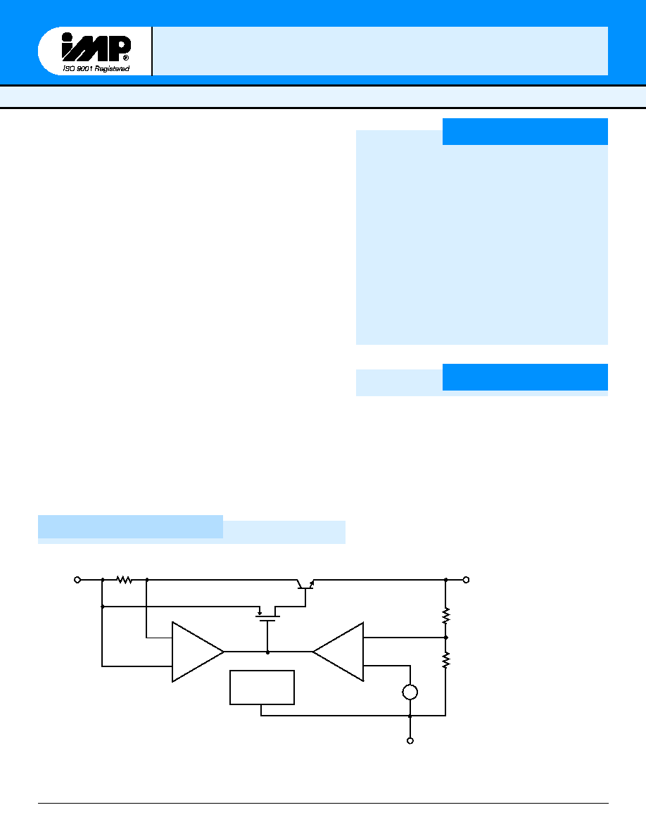
Block Diagram
≠
+
+
≠
37_01.eps
GND
1
Ref
IMP37
Thermal
Protection
Error
Amp
Current
Limit
2
Input
3
Out
(Tab)
R
CS
+
≠
IMP3
IMP3
7
7
P
OWER
M
ANAGEMENT
Lo
Lo
w Dr
w Dr
opout P
opout P
ositiv
ositiv
e
e
V
V
olt
olt
ag
ag
e R
e R
egulat
egulat
or
or
s
s
≠ 800mA
≠ 800mA
≠ 2.5V
≠ 2.5V
, 3.0V and 3.3V Output
, 3.0V and 3.3V Output
The IMP37 series of Low Dropout (LDO) three-terminal voltage regula-
tors feature guaranteed low dropout voltages at currents up to 0.8A. The
IMP37 regulator family dropout voltage is guaranteed to be 0.95V or
lower at 0.8A. At 100mA, the maximum dropout voltage is 0.8V.
Compared with "1117" type LDOs, the IMP37 has a 20% lower dropout
voltage.
Three fixed output voltages are offered: 2.5V, 3.0V and 3.3V. Output volt-
ages are factory trimmed to within 1% of the nominal value.
In addition to low dropout voltages, the IMP37 family features greatly
reduced quiescent operating current. The 75
µ
A maximum specification
represents an over 100 times improvement over competitive devices.
Devices are short circuit protected, and a thermal protection circuit shuts
the regulator off should the junction temperature exceed 165∞C.
The IMP37 is available in low-profile plastic SOT-223 and TO-263
packages and are pin compatible with fixed "1117" devices.

2
408-432-9100/www.impweb.com
©
1999 IMP, Inc.
Pin Configuration
IMP3
IMP3
7
7
Pin Descriptions
IMP37
GND
INPUT
TAB IS V
OUT
1
3
OUT
2
37_04.eps
Package Marking Code
Ordering Information
IMP37
37_05.eps
GND
INPUT
1
3
OUT
TAB IS V
OUT
2
SOT-223
TO-263
Front View
Front View
r
e
b
m
u
N
t
r
a
P
e
g
a
k
c
a
P
e
c
i
v
e
D
g
n
i
k
r
a
M
T
S
J
5
2
-
7
3
P
M
I
3
2
2
-
T
O
S
5
2
7
3
T
S
J
0
3
-
7
3
P
M
I
3
2
2
-
T
O
S
0
3
7
3
T
S
J
3
3
-
7
3
P
M
I
3
2
2
-
T
O
S
3
3
7
3
M
C
J
5
2
-
7
3
P
M
I
3
6
2
-
O
T
M
C
J
5
2
7
3
M
C
J
0
3
-
7
3
P
M
I
3
6
2
-
O
T
M
C
J
0
3
7
3
M
C
J
3
3
-
7
3
P
M
I
3
6
2
-
O
T
M
C
J
3
3
7
3
s
p
e
.
5
0
e
l
b
a
T
_
7
3
s
n
o
i
t
p
O
t
u
p
t
u
O
r
e
b
m
u
N
g
n
i
r
e
d
r
O
t
r
a
P
e
g
a
t
l
o
V
m
u
m
i
x
a
M
t
n
e
r
r
u
C
t
n
e
c
s
e
i
u
Q
t
a
e
g
a
t
l
o
V
t
u
o
p
o
r
D
A
m
0
0
8
3
2
2
-
T
O
S
e
g
a
k
c
a
P
3
6
2
-
O
T
e
g
a
k
c
a
P
V
5
.
2
5
7
µ
A
V
5
9
.
0
T
S
J
5
2
-
7
3
P
M
I
M
C
J
5
2
-
7
3
P
M
I
V
0
.
3
5
7
µ
A
V
5
9
.
0
T
S
J
0
3
-
7
3
P
M
I
M
C
J
0
3
-
7
3
P
M
I
V
3
.
3
5
7
µ
A
V
5
9
.
0
T
S
J
3
3
-
7
3
P
M
I
M
C
J
3
3
-
7
3
P
M
I
s
p
e
.
6
0
t
_
7
3
Note: Tape and reel shipping is available for the SOT-223 and TO-263 packages. Append the TAPE AND REEL designation "/T" to the ordering
part number for tape and reel devices. For example, the IMP37-25JST/T is a 2.5V SOT-223 packaged device shipped in reels.
r
e
b
m
u
N
n
i
P
e
m
a
N
n
o
i
t
c
n
u
F
1
D
N
G
n
i
P
d
n
u
o
r
G
2
T
U
O
e
g
a
t
l
o
V
t
u
p
t
u
O
3
T
U
P
N
I
e
g
a
t
l
o
V
t
u
p
n
I
B
A
T
B
A
T
e
g
a
t
l
o
V
t
u
p
t
u
O
s
p
e
.
3
0
e
l
b
a
T
_
7
3

©
1999 IMP, Inc.
408-432-9100/www.impweb.com
3
IMP3
IMP3
7
7
Absolute Maximum Ratings
Electrical Characteristics
Input Voltage . . . . . . . . . . . . . . . . . . . . . . . . . 7V
Operating Junction Temperature . . . . . . . . . 0
∞
C to 150
∞
C
Storage Temperature Range . . . . . . . . . . . . . ≠65
∞
C to +150
∞
C
Lead Temperature (Soldering) . . . . . . . . . . . . . 300
∞
C for 10 seconds
These are stress ratings only and functional operation is not implied.
Exposure to absolute maximum ratings for prolonged time periods may
affect device reliability. All voltages are with respect to ground.
Specifications apply over the junction operating temperature range of T
J
= 0∞C to +125∞C unless otherwise noted.
Notes: 1. See thermal regulation specification for changes in output voltage due to heating effects. Load regulation and line regulation
are measured with low duty cycle pulse testing to maintain a constant junction temperature.
2. Dropout voltage is specified over the full output current range. Dropout voltage is defined as the minimum input/output
differential measured at the specified output current.
3. Minimum load current is defined as the minimum output current required to maintain regulation.
r
e
t
e
m
a
r
a
P
l
o
b
m
y
S
x
if
f
u
S
s
n
o
it
i
d
n
o
C
n
i
M
p
y
T
x
a
M
s
ti
n
U
e
g
a
t
l
o
V
t
u
p
t
u
O
V
T
U
O
5
2
≠
I
T
U
O
V
,
A
m
0
1
=
N
I
T
,
V
5
8
.
4
=
J
5
2
=
C
∞
5
7
4
.
2
5
.
2
5
2
5
.
2
V
A
m
0
1
I
T
U
O
I
X
A
M
V
5
2
.
4
,
V
N
I
V
5
.
5
5
4
.
2
5
.
2
5
5
.
2
0
3
≠
I
T
U
O
V
,
A
m
0
1
=
N
I
T
,
V
5
=
J
5
2
=
C
∞
7
9
.
2
0
0
.
3
3
0
.
3
A
m
0
1
I
T
U
O
I
X
A
M
V
5
7
.
4
,
V
N
I
V
5
.
5
4
9
.
2
0
0
.
3
6
0
.
3
3
3
≠
I
T
U
O
V
,
A
m
0
1
=
N
I
T
,
V
5
=
J
5
2
=
C
∞
7
6
2
.
3
0
3
.
3
3
3
3
.
3
A
m
0
1
I
T
U
O
I
X
A
M
V
5
7
.
4
,
V
N
I
V
5
.
5
5
3
2
.
3
0
3
.
3
5
6
3
.
3
n
o
i
t
a
l
u
g
e
R
e
n
i
L
)
1
e
t
o
N
(
5
2
≠
I
T
U
O
V
5
2
.
4
,
A
m
0
1
=
(
V
N
I
)
V
5
.
5
2
1
9
1
V
m
0
3
≠
I
T
U
O
V
5
.
4
,
A
m
0
1
=
V
N
I
V
5
.
5
2
1
9
1
3
3
≠
I
T
U
O
V
5
.
4
,
A
m
0
1
=
V
N
I
V
5
.
5
2
1
9
1
n
o
i
t
a
l
u
g
e
R
e
n
i
L
)
1
e
t
o
N
(
5
2
≠
I
T
U
O
V
5
2
.
4
,
A
m
0
1
=
(
V
N
I
)
T
,
V
5
.
5
A
5
2
=
C
∞
8
.
2
3
.
4
V
m
0
3
≠
I
T
U
O
V
5
.
4
,
A
m
0
1
=
V
N
I
T
,
V
5
.
5
A
5
2
=
C
∞
8
.
2
3
.
4
3
3
≠
I
T
U
O
V
5
.
4
,
A
m
0
1
=
V
N
I
T
,
V
5
.
5
A
5
2
=
C
∞
8
.
2
3
.
4
n
o
i
t
a
l
u
g
e
R
d
a
o
L
)
1
e
t
o
N
(
5
2
≠
V
N
I
A
m
5
,
V
5
2
.
4
=
I
T
U
O
A
m
0
0
8
5
2
0
3
V
m
0
3
≠
V
N
I
A
m
5
,
V
5
7
.
4
=
I
T
U
O
A
m
0
0
8
5
2
0
3
3
3
≠
V
N
I
A
m
5
,
V
5
7
.
4
=
I
T
U
O
A
m
0
0
8
5
2
0
3
e
g
a
t
l
o
V
t
u
o
p
o
r
D
)
2
e
t
o
N
(
x
x
≠
I
T
U
O
A
m
0
0
1
=
8
.
0
V
I
T
U
O
A
m
0
0
8
=
5
9
.
0
t
i
m
i
L
t
n
e
r
r
u
C
I
)
X
A
M
(
T
U
O
x
x
≠
T
J
5
2
=
C
∞
0
0
8
0
5
9
0
0
2
1
A
m
t
n
e
r
r
u
C
d
a
o
L
m
u
m
i
n
i
M
x
x
≠
0
.
5
A
m
t
n
e
r
r
u
C
t
n
e
c
s
e
i
u
Q
I
Q
x
x
≠
V
N
I
V
6
6
3
5
7
µ
A
n
o
i
t
a
l
u
g
e
R
l
a
m
r
e
h
T
T
A
5
2
=
C
∞
e
s
l
u
P
s
m
0
3
,
1
0
.
0
1
.
0
W
/
%
n
o
i
t
c
e
j
e
R
e
l
p
p
i
R
f
E
L
P
P
I
R
V
,
z
H
0
2
1
=
N
I
T
,
V
5
=
A
5
2
=
C
∞
V
E
L
P
P
I
R
I
,
p
-
p
V
1
=
D
A
O
L
A
m
0
1
=
1
5
4
5
B
d
y
t
il
i
b
a
t
S
e
r
u
t
a
r
e
p
m
e
T
5
.
0
%
y
t
il
i
b
a
t
S
m
r
e
T
g
n
o
L
T
A
5
2
1
=
C
∞
s
r
H
0
0
0
1
,
3
.
0
%
e
s
i
o
N
t
u
p
t
u
O
S
M
R
V
f
o
%
(
T
U
O
z
H
0
1
,
)
f
T
,
z
H
k
0
1
J
5
2
=
C
∞
3
0
0
.
0
%
e
c
n
a
t
s
i
s
e
R
l
a
m
r
e
h
T
)
3
2
2
-
O
T
(
B
A
T
t
a
e
s
a
C
-
o
t
-
n
o
i
t
c
n
u
J
5
1
∞
W
/
C
)
3
6
2
-
O
T
(
B
A
T
t
a
e
s
a
C
-
o
t
-
n
o
i
t
c
n
u
J
0
1
s
p
e
.
7
0
t
_
7
3

4
408-432-9100/www.impweb.com
©
1999 IMP, Inc.
IMP3
IMP3
7
7
Application Information
The IMP37 voltage regulator ICs offer self-protection features
which include short-circuit current protection and automatic thermal
shutdown (for junction temperature above 165∞C).
Circuit Stability
Like all regulators, an output filter capacitor is required for circuit sta-
bility. Besides smoothing the output, the output capacitor
"completes" the regulator's frequency compensation. The ESR of the
output capacitor should be less than 0.5
. Low ESR capacitors are
preferred.
Table 1 shows recommended minimum capacitance values for both
aluminum and tantalum capacitors. Larger values of output capaci-
tance do not cause stability problems.
Table 1. Recommended Output Bypass Capacitors
An input bypass capacitor is recommended. A 10
µ
F or larger tanta-
lum capacitor is suitable for most applications.
5
.
0
<
R
S
E
(
r
o
t
i
c
a
p
a
C
s
s
a
p
y
B
t
u
p
t
u
O
)
0
1
µ
0
0
1
,
m
u
l
a
t
n
a
T
F
µ
m
u
n
i
m
u
l
A
F
Figure 1. Fixed 3.3V Regulator
Thermal Management
The maximum operating junction temperature for the IMP37 devices
is 150∞C. The junction temperature can be calculated when the
power dissipation and ambient temperature are known with this
equation: T
J
= T
A
+ (P
D
x
JA
).
The thermal resistance from juntion-to-ambient (
JA
) is the sum of
the three thermal resistances:
JA
=
JT
+
TS
+
SA
Where
JT
= Junction-to-Tab thermal resistance
TS
= Tab-to-Heat Sink thermal resistance
SA
= Heat Sink-to-Air thermal resistance
Table 2. Thermal Resistance of Packages
The IMP37 series devices have thermal limiting circuitry to protect
the device from over current. For continuous operation, the maxi-
mum junction temperature rating must not be exceeded.
e
p
y
T
e
g
a
k
c
a
P
e
c
n
a
t
s
i
s
e
R
l
a
m
r
e
h
T
,
b
a
T
o
t
n
o
i
t
c
n
u
J
T
J
3
2
2
-
T
O
S
5
1 ∞
W
/
C
3
6
2
-
O
T
0
1 ∞
W
/
C
IMP37
OUT
V
IN
*
**
IN
3.3V
37_02.eps
GND
* Min. 15
µ
F Tantalum or 100
µ
F Aluminum.
Capacitor May Be Increased Without Limit.
** 10
µ
F Tantalum or 100
µ
F Aluminum
+
+

©
1999 IMP, Inc.
408-432-9100/www.impweb.com
1
Key Features
Applications
x
Pagers
x
Cellular/GSM/PHS Phones
x
Instrumentation
x
Wireless Terminals
x
Battery Powered Systems
x
Medical Instruments
x
Linear Post-Regulators
x
Pin Compatible with TelCom TC1014/1015/1185
x
Lower Dropout Voltage for Long Battery Life
≠ IMP2014: 70mV vs. TelCom TC1014 120mV
≠ IMP2015: 160mV vs. TelCom TC1015 250mV
≠ IMP2185: 250mV vs. TelCom TC1185 400mV
x
Power Saving Shutdown Mode
≠ 0.2µA shutdown current
x
Superior Load Regulation
≠ 0.32%
x
Long Battery Life
≠ 33µA no load ground current
x
Accurate Output Voltage
≠ ± 2.5% over temperature
x
Low Drift Output: 40ppm/
∞
C
x
Guaranteed Minimum Output Current
≠ IMP2014: 60mA
≠ IMP2015: 110mA
≠ IMP2185: 160mA
x
Over-Current and Over-Temperature Protection
x
Reference Bypass Input for Low-noise and
Improved PSRR
x
Compact SOT-23A-5 Package
IMP20
IMP20
1
1
4/1
4/1
5, IMP2
5, IMP2
1
1
85
85
P
OWER
M
ANAGEMENT
60mA/1
60mA/1
1
1
0mA/1
0mA/1
60mA
60mA
Super Lo
Super Lo
w Dr
w Dr
opout CMOS
opout CMOS
R
R
egulat
egulat
or
or
s wit
s wit
h Batt
h Batt
er
er
y Lif
y Lif
e
e
Ext
Ext
ending Shutdo
ending Shutdo
wn Mode
wn Mode
The IMP2014, IMP2015 and IMP2185 high performance CMOS low
dropout voltage regulators offer superior dropout voltage performance
and load regulation characteristics as compared to the pin compatible
TC1014/1015/1185 devices offered by TelCom Semiconductor. Dropout
voltage performance has been improved by up to 40%.
Load regulation and power supply PSRR have been optimized. Load
regulation is typically 0.32% and PSRR is 53dB at 1kHz.
A logic input controlled shutdown mode extends system battery life by
reducing quiescent current to 0.2
µ
A maximum. The shutdown mode can
be initiated by a system microcontroller.
The regulators were designed with ease of use and stability in mind.
Stability is guaranteed for 0.47
µ
F and greater load capacitors with an
ESR up to 5
. Ceramic or tantalum capacitors can be used.
Three devices with different guaranteed output current specifications
are available: IMP2014 (60mA), IMP2015 (110mA) and IMP2185
(160mA). Each device has output voltage options of 2.5V, 2.7V, 2.85V,
3.0V, 3.3V, 3.6V and 4.0V.
Typical Application
0.01
µ
F/3.3
µ
F
(optional)
1
µ
F
1
µ
F
+
V
IN
V
OUT
IMP2014
IMP2015
IMP2185
BYPASS
Shutdown*
Control
1
3
5
4
2
SHDN
2014/15_02.eps
GND
V
OUT
* Tie to V
IN
if not used.

2
408-432-9100/www.impweb.com
©
1999 IMP, Inc.
IMP20
IMP20
1
1
4/1
4/1
5, IMP2
5, IMP2
1
1
85
85
IMP2014/15
IMP2185
V
IN
SHDN
1
V
OUT
5
3
BYPASS
4
GND
2
2014/15_01.eps
SOT-23A
*
r
e
b
m
u
N
t
r
a
P
e
g
a
k
c
a
P
t
u
p
t
u
O
e
g
a
t
l
o
V
)
V
(
t
u
p
t
u
O
t
n
e
r
r
u
C
)
A
m
(
n
w
o
d
t
u
h
S
n
i
P
t
s
u
j
d
A
n
i
P
Y
A
K
O
g
a
l
F
t
u
p
t
u
O
e
c
n
e
r
e
f
e
R
n
i
P
s
s
a
p
y
B
g
n
i
k
r
a
M
e
g
a
k
c
a
P
A
B
C
D
T
/
K
U
J
5
.
2
-
4
1
0
2
P
M
I
5
-
A
3
2
T
O
S
5
.
2
0
6
M
A
x
x
T
/
K
U
J
7
.
2
-
4
1
0
2
P
M
I
5
-
A
3
2
T
O
S
7
.
2
0
6
M
B
x
x
T
/
K
U
J
5
8
.
2
-
4
1
0
2
P
M
I
5
-
A
3
2
T
O
S
5
8
.
2
0
6
M
C
x
x
T
/
K
U
J
0
.
3
-
4
1
0
2
P
M
I
5
-
A
3
2
T
O
S
0
.
3
0
6
M
D
x
x
T
/
K
U
J
3
.
3
-
4
1
0
2
P
M
I
5
-
A
3
2
T
O
S
3
.
3
0
6
M
E
x
x
T
/
K
U
J
6
.
3
-
4
1
0
2
P
M
I
5
-
A
3
2
T
O
S
6
.
3
0
6
M
F
x
x
T
/
K
U
J
0
.
4
-
4
1
0
2
P
M
I
5
-
A
3
2
T
O
S
0
.
4
0
6
M
G
x
x
T
/
K
U
J
5
.
2
-
5
1
0
2
P
M
I
5
-
A
3
2
T
O
S
5
.
2
0
1
1
O
A
x
x
T
/
K
U
J
7
.
2
-
5
1
0
2
P
M
I
5
-
A
3
2
T
O
S
7
.
2
0
1
1
O
B
x
x
T
/
K
U
J
5
8
.
2
-
5
1
0
2
P
M
I
5
-
A
3
2
T
O
S
5
8
.
2
0
1
1
O
C
x
x
T
/
K
U
J
0
.
3
-
5
1
0
2
P
M
I
5
-
A
3
2
T
O
S
0
.
3
0
1
1
O
D
x
x
T
/
K
U
J
3
.
3
-
5
1
0
2
P
M
I
5
-
A
3
2
T
O
S
3
.
3
0
1
1
O
E
x
x
T
/
K
U
J
6
.
3
-
5
1
0
2
P
M
I
5
-
A
3
2
T
O
S
6
.
3
0
1
1
O
F
x
x
T
/
K
U
J
0
.
4
-
5
1
0
2
P
M
I
5
-
A
3
2
T
O
S
0
.
4
0
1
1
O
G
x
x
T
/
K
U
J
5
.
2
-
5
8
1
2
P
M
I
5
-
A
3
2
T
O
S
5
.
2
0
6
1
X
A
x
x
T
/
K
U
J
7
.
2
-
5
8
1
2
P
M
I
5
-
A
3
2
T
O
S
7
.
2
0
6
1
X
B
x
x
T
/
K
U
J
5
8
.
2
-
5
8
1
2
P
M
I
5
-
A
3
2
T
O
S
5
8
.
2
0
6
1
X
C
x
x
T
/
K
U
J
0
.
3
-
5
8
1
2
P
M
I
5
-
A
3
2
T
O
S
0
.
3
0
6
1
X
D
x
x
T
/
K
U
J
3
.
3
-
5
8
1
2
P
M
I
5
-
A
3
2
T
O
S
3
.
3
0
6
1
X
E
x
x
T
/
K
U
J
6
.
3
-
5
8
1
2
P
M
I
5
-
A
3
2
T
O
S
6
.
3
0
6
1
X
F
x
x
T
/
K
U
J
0
.
4
-
5
8
1
2
P
M
I
5
-
A
3
2
T
O
S
0
.
4
0
6
1
X
G
x
x
l
e
e
R
d
n
a
e
p
a
T
s
e
t
a
c
i
d
n
i
T
/
*
e
d
o
C
e
t
a
D
=
x
x
s
p
e
.
3
0
t
_
5
1
/
4
1
0
2
r
e
b
m
u
N
n
i
P
e
m
a
N
n
o
i
t
c
n
u
F
1
V
N
I
.
t
u
p
n
i
y
l
p
p
u
s
d
e
t
a
l
u
g
e
r
n
U
2
D
N
G
.
l
a
n
i
m
r
e
t
d
n
u
o
r
G
3
N
D
H
S
g
n
i
r
u
D
.
W
O
L
c
i
g
o
l
a
s
i
N
D
H
S
n
e
h
w
d
e
r
e
t
n
e
s
i
e
d
o
m
n
w
o
d
t
u
h
s
A
.
t
u
p
n
i
l
o
r
t
n
o
c
n
w
o
d
t
u
h
S
0
.
2
o
t
s
p
o
r
d
t
n
e
r
r
u
c
t
n
e
c
s
e
i
u
q
d
n
a
V
0
o
t
s
ll
a
f
e
g
a
t
l
o
v
t
u
p
t
u
o
e
h
t
n
w
o
d
t
u
h
s
µ
.
A
4
S
S
A
P
Y
B
s
e
c
u
d
e
r
d
n
u
o
r
g
o
t
n
i
p
S
S
A
P
Y
B
e
h
t
m
o
r
f
d
e
t
c
e
n
n
o
c
r
o
t
i
c
a
p
a
c
A
.
t
u
p
n
i
s
s
a
p
y
b
e
c
n
e
r
e
f
e
R
R
R
S
P
s
e
c
n
a
h
n
e
d
n
a
e
c
n
e
r
e
f
e
r
l
a
n
r
e
t
n
i
e
h
t
n
o
t
n
e
s
e
r
p
e
s
i
o
n
e
h
t
5
V
T
U
O
e
g
a
t
l
o
v
t
u
p
t
u
O
s
p
e
.
1
0
t
_
5
1
/
4
1
0
2
Pin Configuration
Pin Descriptions
Ordering Information

©
1999 IMP, Inc.
408-432-9100/www.impweb.com
3
IMP20
IMP20
1
1
4/1
4/1
5, IMP2
5, IMP2
1
1
85
85
Input Voltage . . . . . . . . . . . . . . . . . . . . . . . . . 7V
Output Voltage . . . . . . . . . . . . . . . . . . . . . . . . ≠ 0.3V to V
IN
+ 0.3V
Maximum Voltage on Any Pin . . . . . . . . . . . . ≠ 0.3V to (V
IN
+ 0.3V)
Shutdown Voltage (SHDN) . . . . . . . . . . . . . . SHDN
V
IN
+ 0.3V
Operating Junction Temperature Range . . . ≠ 40
∞
C < T
J
< 125
∞
C
Storage Temperature . . . . . . . . . . . . . . . . . . . ≠ 65
∞
C to 150
∞
C
Power Dissipation . . . . . . . . . . . . . . . . . . . . . Internally limited
Note: T
J
= Junction Temperature, T
A
= Ambient Temperature
These are stress ratings only and functional operation is not implied.
Exposure to absolute maximum ratings for prolonged time periods may
affect device reliability. All voltages are with respect to ground.
V
IN
= V
OUT
+1V, I
L
= 100
µ
A, C
L
= 1
µ
F, SHDN > V
IH
, T
A
= 25∞C, unless otherwise noted. Bold/
blue
specifications apply for junction
temperature range ≠40∞C < T
J
< 125∞C.
Notes: 1. V
R
is the regulated output voltage: 2.5V, 2.7V, 2.85V, 3.0V, 3.3V, 3.6V or 4.0V.
2. Dropout Voltage is defined as the difference between IN and OUT when V
R
drops 2% below its nominal value.
3. Specifications which would otherwise be affected by self-heating of the die are tested at a constant die temperature by
using low duty cycle pulse testing.
3. PSRR guaranteed by design.
r
e
t
e
m
a
r
a
P
l
o
b
m
y
S
s
n
o
i
t
i
d
n
o
C
n
i
M
p
y
T
x
a
M
s
t
i
n
U
e
g
n
a
R
e
g
a
t
l
o
V
t
u
p
n
I
V
N
I
0 C
∞
T
<
J
5
2
1
<
C
∞
0
5
.
6
V
≠ 0
4
C
∞
T
<
J
5
2
1
<
C
∞
0
5
.
6
t
n
e
r
r
u
C
t
u
p
t
u
O
m
u
m
i
x
a
M
I
X
A
M
O
4
1
0
2
P
M
I
0
6
A
m
5
1
0
2
P
M
I
0
1
1
5
8
1
2
P
M
I
0
6
1
e
g
a
t
l
o
V
t
u
p
t
u
O
d
e
x
i
F
V
T
U
O
1
e
t
o
N
V
R
%
5
.
2
≠
V
R
%
5
.
0
±
V
R
%
5
.
2
+
V
)
2
e
t
o
N
(
e
g
a
t
l
o
V
t
u
o
p
o
r
D
V
N
I
V
-
O
I
L
0
0
1
=
µ
A
1
V
m
I
L
A
m
0
2
=
7
1
3
2
I
L
A
m
0
5
=
0
6
0
7
I
L
)
5
8
1
2
P
M
I
,
5
1
0
2
P
M
I
(
A
m
0
0
1
=
0
9
0
6
1
I
L
)
5
8
1
2
P
M
I
(
A
m
0
5
1
=
3
4
1
0
5
2
t
n
e
r
r
u
C
t
n
e
c
s
e
i
u
Q
)
t
n
e
r
r
u
C
d
n
u
o
r
G
(
d
a
o
l
o
N
3
3
0
5
µ
A
t
n
e
r
r
u
C
y
l
p
p
u
S
n
w
o
d
t
u
h
S
I
D
S
N
I
V
0
=
N
D
H
S
T
J
5
2
C
∞
2
.
0
2
µ
A
t
n
e
i
c
i
f
f
e
o
C
e
r
u
t
a
r
e
p
m
e
T
t
u
p
t
u
O
0
4
m
p
p
/ C
∞
n
o
i
t
a
l
u
g
e
R
l
a
m
r
e
h
T
4
0
.
0
W
/
%
n
o
i
t
a
l
u
g
e
R
e
n
i
L
V
R
V
1
+
V
N
I
V
6
5
7
3
0
.
0
5
3
.
0
%
s
p
e
.
a
2
0
t
_
5
1
/
4
1
0
2
Absolute Maximum Ratings
Electrical Characteristics

4
408-432-9100/www.impweb.com
©
1999 IMP, Inc.
IMP20
IMP20
1
1
4/1
4/1
5, IMP2
5, IMP2
1
1
85
85
V
IN
= V
OUT
+1V, I
L
= 100
µ
A, C
L
= 1
µ
F, SHDN > V
IH
, T
A
= 25∞C, unless otherwise noted. Bold/
blue
specifications apply for junction
temperature range of ≠40∞C < T
J
< 125∞C.
Notes: 1. V
R
is the regulated output voltage: 2.5V, 2.7V, 2.85V, 3.0V, 3.3V, 3.6V or 4.0V.
2. Dropout Voltage is defined as the difference between IN and OUT when V
R
drops 2% below its nominal value.
3. Specifications which would otherwise be affected by self-heating of the die are tested at a constant die temperature by
using low duty cycle pulse testing.
4. PSRR guaranteed by design.
r
e
t
e
m
a
r
a
P
l
o
b
m
y
S
s
n
o
i
t
i
d
n
o
C
n
i
M
p
y
T
x
a
M
s
t
i
n
U
:
n
o
i
t
a
l
u
g
e
R
d
a
o
L
4
1
0
2
P
M
I
I
L
0
0
1
=
µ
A
m
0
5
o
t
A
1
1
.
0
5
.
0
%
5
1
0
2
P
M
I
I
L
0
0
1
=
µ
A
m
0
0
1
o
t
A
6
1
.
0
0
.
1
5
8
1
2
P
M
I
I
L
0
0
1
=
µ
A
m
0
5
1
o
t
A
5
6
.
0
5
.
1
e
i
D
n
w
o
d
t
u
h
S
l
a
m
r
e
h
T
e
r
u
t
a
r
e
p
m
e
T
0
5
1
C
∞
s
i
s
e
r
e
t
s
y
H
n
w
o
d
t
u
h
S
l
a
m
r
e
h
T
2
1
C
∞
n
o
i
t
c
e
j
e
R
e
l
p
p
i
R
R
R
S
P
V
N
I
V
(
O
)
V
1
+
±
V
5
2
.
0
C
O
3
.
3
=
µ
c
i
m
a
r
e
c
F
C
S
S
A
P
Y
B
1
0
.
0
=
µ
F
=
.
q
e
r
F
z
H
k
1
0
6
B
d
=
.
q
e
r
F
z
H
k
0
1
7
4
=
.
q
e
r
F
z
H
M
1
4
3
e
s
i
o
N
t
u
p
t
u
O
z
H
k
0
5
o
t
z
H
0
0
3
r
o
t
i
c
a
p
a
c
s
s
a
p
y
b
o
N
I
L
)
4
1
0
2
P
M
I
(
A
m
0
5
=
I
L
A
m
0
0
1
=
0
8
2
µ
V
S
M
R
z
H
k
0
5
o
t
z
H
0
0
3
C
S
S
A
P
Y
B
1
0
.
0
=
µ
F
I
L
)
4
1
0
2
P
M
I
(
A
m
0
5
=
I
L
A
m
0
0
1
=
0
6
µ
V
S
M
R
d
l
o
h
s
e
r
h
T
H
G
I
H
t
u
p
n
I
N
D
H
S
V
5
.
2
V
N
I
V
5
.
6
5
4
V
f
o
%
N
I
d
l
o
h
s
e
r
h
T
W
O
L
t
u
p
n
I
N
D
H
S
V
5
.
2
V
N
I
V
5
.
6
5
1
V
f
o
%
N
I
V
o
t
n
i
t
n
e
r
r
u
C
e
s
r
e
v
e
R
T
U
O
V
)
N
I
(
V
<
)
T
U
O
(
V
=
H
G
I
H
=
N
D
H
S
N
I
0
.
2
A
m
V
)
N
I
(
V
<
)
T
U
O
(
W
O
L
=
N
D
H
S
7
.
2
µ
A
t
i
m
i
L
t
n
e
r
r
u
C
t
u
p
t
u
O
0
5
3
0
0
6
A
m
s
p
e
.
b
2
0
t
_
5
1
/
4
1
0
2
Electrical Characteristics

IMP20
IMP20
1
1
4/1
4/1
5, IMP2
5, IMP2
1
1
85
85
Typical Characteristics
©
1999 IMP, Inc.
408-432-9100/www.impweb.com
5
Figure 1. Line Transient Response
Figure 2. Enable Input Response
V
OUT
2014/15_12.eps
50mV/DIV
20
µ
s/DIV
V
IN
= 1V
0V
Output
2014/15_13.eps
1V/DIV
5V/DIV
100
µ
s/DIV
0V
Enable
Figure 3. Load Transient Response (50mA Step)
Figure 4. Load Transient Response (100mA Step)
V
OUT
2014/15_09.eps
25mV/DIV
20mA/DIV
50
µ
s/DIV
Load
Pulse
V
OUT
2014/15_10.eps
25mV/DIV
50mA/DIV
50
µ
s/DIV
Load
Pulse
Figure 5. Output Short Circuit Response
2014/15_11.eps
100mA/DIV
100ms/DIV

IMP20
IMP20
1
1
4/1
4/1
5, IMP2
5, IMP2
1
1
85
85
Application Information
6
408-432-9100/www.impweb.com
©
1999 IMP, Inc.
The IMP2014, IMP2015 and IMP2185 have been designed to offer
exceptionally low dropout voltage, superior load regulation and
minimum quiescent power.
Shutdown Mode
A battery-life-extending mode is available. Through the active
LOW shutdown pin, SHDN, the regulator can be enabled or
turned off. The regulator is shutdown (turned off) when SHDN is
LOW and enabled (turned on) when SHDN is HIGH.
The shutdown signal can be supplied from a CMOS gate or from
an I/O port of a microcontroller.
During shutdown, the output voltage falls to 0V and the supply
current is typically only 200nA.
If the shutdown mode is not needed, SHDN should be connected
directly to the regulator input voltage pin.
Output Capacitor
The IMP2014, IMP2015 and IMP2185 were designed for stable
operation with a wide range of capacitor values and type. The
output capacitor should be above 0.47
µ
F. A 1
µ
F value is recom-
mended. Ceramic or tantalum capacitors are suitable with an ESR
of up to 5
.
Reference Voltage Bypass Capacitor
For low noise operation a 0.01
µ
F or larger capacitor can be con-
nected from the BYPASS pin to ground. For maximum power sup-
ply rejection/line rejection, a 3.3
µ
F value is suggested.
The IMP2014/2015/2185 were designed so that line regulation
and ripple rejection would be maximized. This was accomplished
by powering the internal bandgap reference from an internal reg-
ulated source. This "pre-regulation" greatly improves power sup-
ply regulation for input voltages greater than that of the internal
voltage regulator, 3.5V.
Thermal Shutdown
An on-chip thermal protection circuit shuts the LDO regulator off
when the die temperature exceeds 150
∞
C. There is a built in 12
∞
C
hysteresis. The regulator will remain off until the die temperature
drops to approximately to 138
∞
C.

©
1999 IMP, Inc.
408-432-9100/www.impweb.com
1
Key Features
Applications
x
Pagers
x
Cellular/GSM/PHS Phones
x
Instrumentation
x
Wireless Terminals
x
Battery Powered Systems
x
Medical Instruments
x
Linear Post-Regulators
x
Pin Compatible with TelCom TC1054/1055/1186
x
Lower Dropout Voltage for Long Battery Life
≠ IMP2054: 70mV vs. TelCom TC1054 120mV
≠ IMP2055: 160mV vs. TelCom TC1055 250mV
≠ IMP2186: 250mV vs. TelCom TC1186 400mV
x
Power Saving Shutdown Mode
≠ 0.2µA shutdown current
x
ERROR Output
≠ Low battery detection
≠ Processor reset
x
Superior Load Regulation
≠ 0.32%
x
Long Battery Life
≠ 33µA no load ground current
x
Accurate Output Voltage
≠ ± 2.5% over temperature
x
Low Drift Output: 40ppm/
∞
C
x
Guaranteed Minimum Output Current
≠ IMP2054: 60mA
≠ IMP2055: 110mA
≠ IMP2186: 160mA
x
Over-Current and Over-Temperature Protection
x
Compact SOT-23A-5 Package
IMP205
IMP205
4/55, IMP2
4/55, IMP2
1
1
86
86
P
OWER
M
ANAGEMENT
60mA/1
60mA/1
1
1
0mA/1
0mA/1
60mA
60mA
Super Lo
Super Lo
w Dr
w Dr
opout CMOS
opout CMOS
R
R
egulat
egulat
or
or
s wit
s wit
h Batt
h Batt
er
er
y Lif
y Lif
e
e
Ext
Ext
ending Shutdo
ending Shutdo
wn Mode and
wn Mode and
ERR
ERR
OR Output
OR Output
The IMP2054, IMP2055 and IMP2186 high performance CMOS low
dropout voltage regulators offer superior dropout voltage performance
and load regulation characteristics as compared to the pin compatible
TC1054/1055/1186 devices offered by TelCom Semiconductor. Dropout
voltage performance has been improved by up to 40%.
Load regulation and power supply PSRR have been optimized. Load
regulation is typically 0.32% and PSRR is 53dB at 1kHz.
A logic input controlled shutdown mode extends system battery life by
reducing quiescent current to 0.2
µ
A maximum. The shutdown mode can
be initiated by a system microcontroller.
The regulators were designed with ease of use and stability in mind.
Stability is guaranteed for 0.47
µ
F and greater load capacitors with an
ESR up to 5
. Ceramic or tantalum capacitors can be used.
Three devices with different guaranteed output current specifications
are available: IMP2054 (60mA), IMP2055 (110mA) and IMP2186
(160mA). Each device has output voltage options of 2.5V, 2.7V, 2.85V,
3.0V, 3.3V, 3.6V and 4.0V.
Typical Application
1
µ
F
1M
1
µ
F
+
V
IN
V
OUT
IMP2054
IMP2055
IMP2186
ERROR
Shutdown*
Control
1
3
5
4
2
SHDN
2054/55_02.eps
GND
V
OUT
* Tie to V
IN
if not used.

2
408-432-9100/www.impweb.com
©
1999 IMP, Inc.
IMP205
IMP205
4/55, IMP2
4/55, IMP2
1
1
86
86
IMP2054/55
IMP2186
V
IN
SHDN
1
V
OUT
5
3
ERROR
4
GND
2
2054/55_01.eps
SOT-23A
*
r
e
b
m
u
N
t
r
a
P
e
g
a
k
c
a
P
t
u
p
t
u
O
e
g
a
t
l
o
V
)
V
(
t
u
p
t
u
O
t
n
e
r
r
u
C
)
A
m
(
n
w
o
d
t
u
h
S
n
i
P
t
s
u
j
d
A
n
i
P
R
O
R
R
E
g
a
l
F
t
u
p
t
u
O
e
c
n
e
r
e
f
e
R
n
i
P
s
s
a
p
y
B
g
n
i
k
r
a
M
e
g
a
k
c
a
P
A
B
C
D
T
/
K
U
J
5
.
2
-
4
5
0
2
P
M
I
5
-
A
3
2
T
O
S
5
.
2
0
6
R
A
x
x
T
/
K
U
J
7
.
2
-
4
5
0
2
P
M
I
5
-
A
3
2
T
O
S
7
.
2
0
6
R
B
x
x
T
/
K
U
J
5
8
.
2
-
4
5
0
2
P
M
I
5
-
A
3
2
T
O
S
5
8
.
2
0
6
R
C
x
x
T
/
K
U
J
0
.
3
-
4
5
0
2
P
M
I
5
-
A
3
2
T
O
S
0
.
3
0
6
R
D
x
x
T
/
K
U
J
3
.
3
-
4
5
0
2
P
M
I
5
-
A
3
2
T
O
S
3
.
3
0
6
R
E
x
x
T
/
K
U
J
6
.
3
-
4
5
0
2
P
M
I
5
-
A
3
2
T
O
S
6
.
3
0
6
R
F
x
x
T
/
K
U
J
0
.
4
-
4
5
0
2
P
M
I
5
-
A
3
2
T
O
S
0
.
4
0
6
R
G
x
x
T
/
K
U
J
5
.
2
-
5
5
0
2
P
M
I
5
-
A
3
2
T
O
S
5
.
2
0
1
1
T
A
x
x
T
/
K
U
J
7
.
2
-
5
5
0
2
P
M
I
5
-
A
3
2
T
O
S
7
.
2
0
1
1
T
B
x
x
T
/
K
U
J
5
8
.
2
-
5
5
0
2
P
M
I
5
-
A
3
2
T
O
S
5
8
.
2
0
1
1
T
C
x
x
T
/
K
U
J
0
.
3
-
5
5
0
2
P
M
I
5
-
A
3
2
T
O
S
0
.
3
0
1
1
T
D
x
x
T
/
K
U
J
3
.
3
-
5
5
0
2
P
M
I
5
-
A
3
2
T
O
S
3
.
3
0
1
1
T
E
x
x
T
/
K
U
J
6
.
3
-
5
5
0
2
P
M
I
5
-
A
3
2
T
O
S
6
.
3
0
1
1
T
F
x
x
T
/
K
U
J
0
.
4
-
5
5
0
2
P
M
I
5
-
A
3
2
T
O
S
0
.
4
0
1
1
T
G
x
x
T
/
K
U
J
5
.
2
-
6
8
1
2
P
M
I
5
-
A
3
2
T
O
S
5
.
2
0
6
1
Y
A
x
x
T
/
K
U
J
7
.
2
-
6
8
1
2
P
M
I
5
-
A
3
2
T
O
S
7
.
2
0
6
1
Y
B
x
x
T
/
K
U
J
5
8
.
2
-
6
8
1
2
P
M
I
5
-
A
3
2
T
O
S
5
8
.
2
0
6
1
Y
C
x
x
T
/
K
U
J
0
.
3
-
6
8
1
2
P
M
I
5
-
A
3
2
T
O
S
0
.
3
0
6
1
Y
D
x
x
T
/
K
U
J
3
.
3
-
6
8
1
2
P
M
I
5
-
A
3
2
T
O
S
3
.
3
0
6
1
Y
E
x
x
T
/
K
U
J
6
.
3
-
6
8
1
2
P
M
I
5
-
A
3
2
T
O
S
6
.
3
0
6
1
Y
F
x
x
T
/
K
U
J
0
.
4
-
6
8
1
2
P
M
I
5
-
A
3
2
T
O
S
0
.
4
0
6
1
Y
G
x
x
l
e
e
R
d
n
a
e
p
a
T
s
e
t
a
c
i
d
n
i
T
/
*
e
d
o
C
e
t
a
D
=
x
x
s
p
e
.
3
0
t
_
5
5
/
4
5
0
2
r
e
b
m
u
N
n
i
P
e
m
a
N
n
o
i
t
c
n
u
F
1
V
N
I
.
t
u
p
n
i
y
l
p
p
u
s
d
e
t
a
l
u
g
e
r
n
U
2
D
N
G
.
l
a
n
i
m
r
e
t
d
n
u
o
r
G
3
N
D
H
S
g
n
i
r
u
D
.
W
O
L
c
i
g
o
l
a
s
i
N
D
H
S
n
e
h
w
d
e
r
e
t
n
e
s
i
e
d
o
m
n
w
o
d
t
u
h
s
A
.
t
u
p
n
i
l
o
r
t
n
o
c
n
w
o
d
t
u
h
S
0
.
2
o
t
s
p
o
r
d
t
n
e
r
r
u
c
t
n
e
c
s
e
i
u
q
d
n
a
V
0
o
t
s
ll
a
f
e
g
a
t
l
o
v
t
u
p
t
u
o
e
h
t
n
w
o
d
t
u
h
s
µ
.
A
4
R
O
R
R
E
s
i
t
u
p
t
u
o
e
h
t
n
e
h
w
W
O
L
s
e
o
g
t
a
h
t
t
u
p
t
u
o
n
i
a
r
d
n
e
p
o
n
A
.
t
u
p
t
u
o
g
a
l
F
n
o
i
t
a
l
u
g
e
R
-
f
o
-
t
u
O
.
%
5
y
l
e
t
a
m
i
x
o
r
p
p
a
y
b
e
c
n
a
r
e
l
o
t
-
f
o
-
t
u
o
5
V
T
U
O
e
g
a
t
l
o
v
t
u
p
t
u
O
s
p
e
.
1
0
t
_
5
5
/
4
5
0
2
Pin Configuration
Pin Descriptions
Ordering Information

©
1999 IMP, Inc.
408-432-9100/www.impweb.com
3
IMP205
IMP205
4/55, IMP2
4/55, IMP2
1
1
86
86
Input Voltage . . . . . . . . . . . . . . . . . . . . . . . . . 7V
Output Voltage . . . . . . . . . . . . . . . . . . . . . . . . ≠ 0.3V to V
IN
+ 0.3V
Maximum Voltage on Any Pin . . . . . . . . . . . . ≠ 0.3V to (V
IN
+ 0.3V)
Shutdown Voltage (SHDN) . . . . . . . . . . . . . . SHDN
V
IN
+ 0.3V
Operating Junction Temperature Range . . . ≠ 40
∞
C < T
J
< 125
∞
C
Storage Temperature . . . . . . . . . . . . . . . . . . . ≠ 65
∞
C to 150
∞
C
Power Dissipation . . . . . . . . . . . . . . . . . . . . . Internally limited
Note: T
J
= Junction Temperature, T
A
= Ambient Temperature
These are stress ratings only and functional operation is not implied.
Exposure to absolute maximum ratings for prolonged time periods may
affect device reliability. All voltages are with respect to ground.
V
IN
= V
OUT
+1V, I
L
= 100
µ
A, C
L
= 1
µ
F, SHDN > V
IH
, T
A
= 25∞C, unless otherwise noted. Bold/
blue
specifications apply for junction
temperature range ≠40∞C < T
J
< 125∞C.
Notes: 1. V
R
is the regulated output voltage: 2.5V, 2.7V, 2.85V, 3.0V, 3.3V, 3.6V or 4.0V.
2. Dropout Voltage is defined as the difference between IN and OUT when V
R
drops 2% below its nominal value.
3. Specifications which would otherwise be affected by self-heating of the die are tested at a constant die temperature by
using low duty cycle pulse testing.
3. PSRR guaranteed by design.
r
e
t
e
m
a
r
a
P
l
o
b
m
y
S
s
n
o
i
t
i
d
n
o
C
n
i
M
p
y
T
x
a
M
s
t
i
n
U
e
g
n
a
R
e
g
a
t
l
o
V
t
u
p
n
I
V
N
I
0 C
∞
T
<
J
5
2
1
<
C
∞
0
5
.
6
V
≠ 0
4
C
∞
T
<
J
5
2
1
<
C
∞
0
5
.
6
t
n
e
r
r
u
C
t
u
p
t
u
O
m
u
m
i
x
a
M
I
X
A
M
O
4
5
0
2
P
M
I
0
6
A
m
5
5
0
2
P
M
I
0
1
1
6
8
1
2
P
M
I
0
6
1
e
g
a
t
l
o
V
t
u
p
t
u
O
d
e
x
i
F
V
T
U
O
1
e
t
o
N
V
R
%
5
.
2
≠
V
R
%
5
.
0
±
V
R
%
5
.
2
+
V
)
2
e
t
o
N
(
e
g
a
t
l
o
V
t
u
o
p
o
r
D
V
N
I
V
-
O
I
L
0
0
1
=
µ
A
1
V
m
I
L
A
m
0
2
=
7
1
3
2
I
L
A
m
0
5
=
0
6
0
7
I
L
)
6
8
1
2
P
M
I
,
4
5
0
2
P
M
I
(
A
m
0
0
1
=
0
9
0
6
1
I
L
)
6
8
1
2
P
M
I
(
A
m
0
5
1
=
3
4
1
0
5
2
t
n
e
r
r
u
C
t
n
e
c
s
e
i
u
Q
)
t
n
e
r
r
u
C
d
n
u
o
r
G
(
d
a
o
l
o
N
3
3
0
5
µ
A
t
n
e
r
r
u
C
y
l
p
p
u
S
n
w
o
d
t
u
h
S
I
D
S
N
I
V
0
=
N
D
H
S
T
J
5
2
C
∞
2
.
0
2
µ
A
t
n
e
i
c
i
f
f
e
o
C
e
r
u
t
a
r
e
p
m
e
T
t
u
p
t
u
O
0
4
m
p
p
/ C
∞
n
o
i
t
a
l
u
g
e
R
l
a
m
r
e
h
T
4
0
.
0
W
/
%
n
o
i
t
a
l
u
g
e
R
e
n
i
L
V
R
V
1
+
V
N
I
V
6
5
7
3
0
.
0
5
3
.
0
%
s
p
e
.
a
2
0
t
_
5
5
/
4
5
0
2
Absolute Maximum Ratings
Electrical Characteristics

4
408-432-9100/www.impweb.com
©
1999 IMP, Inc.
IMP205
IMP205
4/55, IMP2
4/55, IMP2
1
1
86
86
V
IN
= V
OUT
+1V, I
L
= 100
µ
A, C
L
= 1
µ
F, SHDN > V
IH
, T
A
= 25∞C, unless otherwise noted. Bold/
blue
specifications apply for junction
temperature range of ≠40∞C < T
J
< 125∞C.
Notes: 1. V
R
is the regulated output voltage: 2.5V, 2.7V, 2.85V, 3.0V, 3.3V, 3.6V or 4.0V.
2. Dropout Voltage is defined as the difference between IN and OUT when V
R
drops 2% below its nominal value.
3. Specifications which would otherwise be affected by self-heating of the die are tested at a constant die temperature by
using low duty cycle pulse testing.
4. PSRR guaranteed by design.
r
e
t
e
m
a
r
a
P
l
o
b
m
y
S
s
n
o
i
t
i
d
n
o
C
n
i
M
p
y
T
x
a
M
s
t
i
n
U
:
n
o
i
t
a
l
u
g
e
R
d
a
o
L
4
5
0
2
P
M
I
I
L
0
0
1
=
µ
A
m
0
5
o
t
A
2
3
.
0
0
.
2
%
5
5
0
2
P
M
I
I
L
0
0
1
=
µ
A
m
0
0
1
o
t
A
2
3
.
0
0
.
2
6
8
1
2
P
M
I
I
L
0
0
1
=
µ
A
m
0
5
1
o
t
A
2
3
.
0
0
.
3
e
i
D
n
w
o
d
t
u
h
S
l
a
m
r
e
h
T
e
r
u
t
a
r
e
p
m
e
T
0
5
1
C
∞
s
i
s
e
r
e
t
s
y
H
n
w
o
d
t
u
h
S
l
a
m
r
e
h
T
2
1
C
∞
n
o
i
t
c
e
j
e
R
e
l
p
p
i
R
R
R
S
P
V
N
I
V
(
O
)
V
1
+
±
V
5
2
.
0
C
O
3
.
3
=
µ
c
i
m
a
r
e
c
F
=
.
q
e
r
F
z
H
k
1
8
5
B
d
=
.
q
e
r
F
z
H
k
0
1
5
4
=
.
q
e
r
F
z
H
M
1
4
3
e
s
i
o
N
t
u
p
t
u
O
z
H
k
0
5
o
t
z
H
0
0
3
I
L
)
4
5
0
2
P
M
I
(
A
m
0
5
=
I
L
A
m
0
0
1
=
0
8
2
µ
V
S
M
R
d
l
o
h
s
e
r
h
T
H
G
I
H
t
u
p
n
I
N
D
H
S
V
5
.
2
V
N
I
V
5
.
6
5
4
V
f
o
%
N
I
d
l
o
h
s
e
r
h
T
W
O
L
t
u
p
n
I
N
D
H
S
V
5
.
2
V
N
I
V
5
.
6
5
1
V
f
o
%
N
I
m
u
m
i
n
i
M
g
a
l
F
R
O
R
R
E
e
g
a
t
l
o
V
y
l
p
p
u
S
5
.
1
V
d
l
o
h
s
e
r
h
T
g
a
l
F
R
O
R
R
E
e
g
a
t
l
o
V
V
H
T
V
5
9
.
0
R
V
s
i
s
e
r
e
t
s
y
H
g
a
l
F
R
O
R
R
E
V
S
Y
H
0
5
V
m
w
o
L
t
u
p
t
u
O
g
a
l
F
R
O
R
R
E
e
g
a
t
l
o
V
I
R
O
R
R
E
A
m
1
=
5
7
0
0
4
V
m
V
o
t
n
i
t
n
e
r
r
u
C
e
s
r
e
v
e
R
T
U
O
V
)
N
I
(
V
<
)
T
U
O
(
V
=
H
G
I
H
=
N
D
H
S
N
I
0
.
2
A
m
V
)
N
I
(
V
<
)
T
U
O
(
W
O
L
=
N
D
H
S
7
.
2
µ
A
t
i
m
i
L
t
n
e
r
r
u
C
t
u
p
t
u
O
0
5
3
0
0
6
A
m
s
p
e
.
b
2
0
t
_
5
5
/
4
5
0
2
Electrical Characteristics

IMP205
IMP205
4/55, IMP2
4/55, IMP2
1
1
86
86
Typical Characteristics
©
1999 IMP, Inc.
408-432-9100/www.impweb.com
5
Figure 1. IMP2055 PSRR at I
LOAD
= 100mA
Figure 2. IMP2055 PSRR at I
LOAD
= 1mA
PSRR (dB)
Frequency (Hz)
2054/55_04.eps
1
10
100
1k
10k
100k
10
20
30
40
60
80
50
70
90
PSRR (dB)
Frequency (Hz)
2054/55_05.eps
1
10
100
1k
10k
100k
10
20
30
40
60
80
50
70
100
90
Figure 3. Line Transient Response
Figure 4. Enable Input Response
V
OUT
2054/55_12.eps
50mV/DIV
20
µ
s/DIV
V
IN
= 1V
0V
Output
2054/55_13.eps
1V/DIV
5V/DIV
100
µ
s/DIV
0V
Enable
Figure 5. Load Transient Response (50mA Step)
Figure 6. Load Transient Response (100mA Step)
V
OUT
2054/55_09.eps
25mV/DIV
20mA/DIV
50
µ
s/DIV
Load
Pulse
V
OUT
2054/55_10.eps
25mV/DIV
50mA/DIV
50
µ
s/DIV
Load
Pulse

IMP205
IMP205
4/55, IMP2
4/55, IMP2
1
1
86
86
Typical Characteristics
Application Information
6
408-432-9100/www.impweb.com
©
1999 IMP, Inc.
2054/55_11.eps
100mA/DIV
100ms/DIV
Figure 7. Output Short Circuit Response
The IMP2054, IMP2055 and IMP2186 have been designed to offer
exceptionally low dropout voltage, superior load regulation and
minimum quiescent power.
Shutdown Mode
A battery-life-extending mode is available. Through the active
LOW shutdown pin, SHDN, the regulator can be enabled or
turned off. The regulator is shutdown (turned off) when SHDN is
LOW and enabled (turned on) when SHDN is HIGH.
The shutdown signal can be supplied from a CMOS gate or from
an I/O port of a microcontroller.
During shutdown, the output voltage falls to 0V and the supply
current is typically only 200nA.
If the shutdown mode is not needed, SHDN should be connected
directly to the regulator input voltage pin.
ERROR Open Drain Output
ERROR is driven low whenever V
OUT
falls out of regulation by
more than 5 percent typically. This condition may be caused by
low input voltage, output current limiting, or thermal limiting.
The ERROR threshold is 5% below rated V
OUT
regardless of the
programmed output voltage value (e.g. ERROR = V
OL
at 4.7V
(typical) for a 5.0V regulator and 2.85V (typical) for a 3.0V regula-
tor). ERROR output operation is shown in Figure 8.
Note that ERROR is active when V
OUT
falls to V
TH
, and inactive
when V
OUT
rises above V
TH
by V
HYS
.
As shown in Figure 9, ERROR can be used as a battery low flag, or
as a microcontroller RESET signal (with the addition of timing
capacitor C 2). R1 x C 2 should be chosen to maintain ERROR
below V
IH
of the processor RESET input for at least 200ms to allow
time for the system to stabilize.
Output Capacitor
The IMP2054, IMP2055 and IMP2186 were designed for stable
operation with a wide range of capacitor values and type. The
output capacitor should be above 0.47
µ
F. A 1
µ
F value is recom-
mended. Ceramic or tantalum capacitors are suitable with an ESR
up to 5
.
Thermal Shutdown
An on-chip thermal protection circuit shuts the LDO regulator off
when the die temperature exceeds 150
∞
C. There is a built in 12
∞
C
hysteresis. The regulator will remain off until the die temperature
drops to approximately to 138
∞
C.

IMP205
IMP205
4/55, IMP2
4/55, IMP2
1
1
86
86
Application Information
©
1999 IMP, Inc.
408-432-9100/www.impweb.com
7
Figure 8. ERROR Output Operation
Figure 9. Typical Application Circuit
1
µ
F
R1
1M
C1
1
µ
F
C2
0.2
µ
F
+
+
+
+
V
IN
V
OUT
IMP2054
IMP2055
IMP2186
ERROR
Shutdown*
Control
1
3
5
4
2
SHDN
2054/55_15.eps
GND
V
OUT
BATTLOW
or RESET
V+
* Tie to V
IN
if unused.
C2 required only if
ERROR is used as
a Processor RESET
Signal (see text).
V
OUT
V
TH
V
IH
V
OL
ERROR
HYSTERESIS (V
HYS
)
2054/55_14.eps

IMP205
IMP205
4/55, IMP2
4/55, IMP2
1
1
86
86
8
408-432-9100/www.impweb.com
©
1999 IMP, Inc.
Notes
Project

©
1999 IMP, Inc.
408-432-9100/www.impweb.com
1
Key Features
Applications
x
Pagers
x
Cellular/GSM/PHS Phones
x
Instrumentation
x
Wireless Terminals
x
Battery Powered Systems
x
Medical Instruments
x
Linear Post-Regulators
x
Pin Compatible with TelCom TC1070/1071/1187
x
Lower Dropout Voltage For Long Battery Life
≠ IMP2070: 70mV vs. TelCom TC1070 120mV
≠ IMP2071: 160mV vs. TelCom TC1071 250mV
≠ IMP2187: 250mV vs. TelCom TC1187 400mV
x
Power Saving Shutdown Mode
≠ 0.2µA shutdown current
x
Adjustable Output Voltage
x
Superior Load Regulation
≠ 0.32%
x
Long Battery Life
≠ 33µA no load ground current
x
Accurate Output Voltage
≠ ± 2.5% over temperature
x
Low Drift Output: 40ppm/
∞
C
x
Guaranteed Minimum Output Current
≠ IMP2070: 60mA
≠ IMP2071: 110mA
≠ IMP2187: 160mA
x
Over-Current and Over-Temperature Protection
x
Compact SOT-23A-5 Package
IMP20
IMP20
70/7
70/7
1
1
, IMP2
, IMP2
1
1
8
8
7
7
P
OWER
M
ANAGEMENT
60mA/1
60mA/1
1
1
0mA/1
0mA/1
60mA
60mA
Super Lo
Super Lo
w Dr
w Dr
opout CMOS
opout CMOS
R
R
egulat
egulat
or
or
s wit
s wit
h Batt
h Batt
er
er
y Lif
y Lif
e
e
Ext
Ext
ending Shutdo
ending Shutdo
wn Mode and
wn Mode and
A
A
djus
djus
t
t
able Output
able Output
The IMP2070, IMP2071 and IMP2187 feature an adjustable output volt-
age. Compared to the pin compatible TC1070/1071/1187 devices offered
by TelCom Semiconductor. Dropout voltage performance has been
improved by up to 40%.
Load regulation and power supply PSRR have been optimized. Load
regulation is typically 0.32% and PSRR is 53dB at 1kHz.
A logic input controlled shutdown mode extends system battery life by
reducing quiescent current to 0.2
µ
A maximum. The shutdown mode can
be initiated by a system microcontroller.
The regulators were designed with ease of use and stability in mind.
Stability is guaranteed for 0.47
µ
F and greater load capacitors with an
ESR up to 5
. Ceramic or tantalum capacitors can be used.
Three devices with different guaranteed output current specifications
are available: IMP2070 (60mA), IMP2071 (110mA) and IMP2187
(160mA).
Typical Application
1
µ
F
R1
R1
R2
1
µ
F
+
R2
V
IN
V
OUT
IMP2070
IMP2071
IMP2187
ADJ
Shutdown*
Control
1
3
5
4
2
SHDN
2070/71_02.eps
GND
V
OUT
V
OUT
= V
REF
◊
1 +
V
REF
= 1.2V
* Tie to V
IN
if not used.

2
408-432-9100/www.impweb.com
©
1999 IMP, Inc.
IMP20
IMP20
70/7
70/7
1
1
, IMP2
, IMP2
1
1
8
8
7
7
IMP2070
IMP2071
IMP2187
V
IN
SHDN
1
V
OUT
5
3
ADJ
4
GND
2
2070/71_01.eps
SOT-23A
*
r
e
b
m
u
N
t
r
a
P
e
g
a
k
c
a
P
t
u
p
t
u
O
e
g
a
t
l
o
V
)
V
(
t
u
p
t
u
O
t
n
e
r
r
u
C
)
A
m
(
n
w
o
d
t
u
h
S
n
i
P
t
s
u
j
d
A
n
i
P
R
O
R
R
E
g
a
l
F
t
u
p
t
u
O
e
c
n
e
r
e
f
e
R
n
i
P
s
s
a
p
y
B
g
n
i
k
r
a
M
e
g
a
k
c
a
P
A
B
C
D
T
/
K
U
J
0
7
0
2
P
M
I
5
-
A
3
2
T
O
S
e
l
b
a
t
s
u
j
d
A
0
6
J
J
x
x
T
/
K
U
J
1
7
0
2
P
M
I
5
-
A
3
2
T
O
S
e
l
b
a
t
s
u
j
d
A
0
1
1
K
J
x
x
T
/
K
U
J
7
8
1
2
P
M
I
5
-
A
3
2
T
O
S
e
l
b
a
t
s
u
j
d
A
0
6
1
L
J
x
x
l
e
e
R
d
n
a
e
p
a
T
s
e
t
a
c
i
d
n
i
T
/
*
e
d
o
C
e
t
a
D
=
x
x
s
p
e
.
3
0
t
_
1
7
/
0
7
0
2
r
e
b
m
u
N
n
i
P
e
m
a
N
n
o
i
t
c
n
u
F
1
V
N
I
.
t
u
p
n
i
y
l
p
p
u
s
d
e
t
a
l
u
g
e
r
n
U
2
D
N
G
.
l
a
n
i
m
r
e
t
d
n
u
o
r
G
3
N
D
H
S
g
n
i
r
u
D
.
W
O
L
c
i
g
o
l
a
s
i
N
D
H
S
n
e
h
w
d
e
r
e
t
n
e
s
i
e
d
o
m
n
w
o
d
t
u
h
s
A
.
t
u
p
n
i
l
o
r
t
n
o
c
n
w
o
d
t
u
h
S
0
.
2
o
t
s
p
o
r
d
t
n
e
r
r
u
c
t
n
e
c
s
e
i
u
q
d
n
a
V
0
o
t
s
ll
a
f
e
g
a
t
l
o
v
t
u
p
t
u
o
e
h
t
n
w
o
d
t
u
h
s
µ
.
A
4
J
D
A
.
l
a
n
i
m
r
e
t
t
n
e
m
t
s
u
j
d
a
e
g
a
t
l
o
v
t
u
p
t
u
O
5
V
T
U
O
.
e
g
a
t
l
o
v
t
u
p
t
u
O
s
p
e
.
1
0
t
_
1
7
/
0
7
0
2
Pin Configuration
Pin Descriptions
Ordering Information

©
1999 IMP, Inc.
408-432-9100/www.impweb.com
3
IMP20
IMP20
70/7
70/7
1
1
, IMP2
, IMP2
1
1
8
8
7
7
Input Voltage . . . . . . . . . . . . . . . . . . . . . . . . . 7V
Output Voltage . . . . . . . . . . . . . . . . . . . . . . . . ≠ 0.3V to V
IN
+ 0.3V
Maximum Voltage on Any Pin . . . . . . . . . . . . ≠ 0.3V to (V
IN
+ 0.3V)
Shutdown Voltage (SHDN) . . . . . . . . . . . . . . SHDN
V
IN
+ 0.3V
Operating Junction Temperature Range . . . ≠ 40
∞
C < T
J
< 125
∞
C
Storage Temperature . . . . . . . . . . . . . . . . . . . ≠ 65
∞
C to 150
∞
C
Power Dissipation . . . . . . . . . . . . . . . . . . . . . Internally limited
Note: T
J
= Junction Temperature, T
A
= Ambient Temperature
These are stress ratings only and functional operation is not implied.
Exposure to absolute maximum ratings for prolonged time periods may
affect device reliability. All voltages are with respect to ground.
V
IN
= V
OUT
+1V, I
L
= 100
µ
A, C
L
= 1
µ
F, SHDN > V
IH
, T
A
= 25∞C, unless otherwise noted. Bold/
blue
specifications apply for junction
temperature range ≠40∞C < T
J
< 125∞C.
Notes: 1. Dropout Voltage is defined as the difference between IN and OUT when V
R
drops 2% below its nominal value.
2. Specifications which would otherwise be affected by self-heating of the die are tested at a constant die temperature by
using low duty cycle pulse testing.
3. PSRR guaranteed by design.
r
e
t
e
m
a
r
a
P
l
o
b
m
y
S
s
n
o
i
t
i
d
n
o
C
n
i
M
p
y
T
x
a
M
s
t
i
n
U
e
g
n
a
R
e
g
a
t
l
o
V
t
u
p
n
I
V
N
I
0 C
∞
T
<
J
5
2
1
<
C
∞
0
5
.
6
V
≠ 0
4
C
∞
T
<
J
5
2
1
<
C
∞
0
5
.
6
t
n
e
r
r
u
C
t
u
p
t
u
O
m
u
m
i
x
a
M
I
X
A
M
O
0
7
0
2
P
M
I
0
6
A
m
1
7
0
2
P
M
I
0
1
1
7
8
1
2
P
M
I
0
6
1
e
g
a
t
l
o
V
t
u
p
t
u
O
e
l
b
a
t
s
u
j
d
A
e
g
n
a
R
V
F
E
R
5
.
5
V
e
g
a
t
l
o
V
e
c
n
e
r
e
f
e
R
V
F
E
R
5
6
1
.
1
0
2
.
1
5
3
2
.
1
V
)
1
e
t
o
N
(
e
g
a
t
l
o
V
t
u
o
p
o
r
D
V
N
I
V
-
O
I
L
0
0
1
=
µ
A
1
V
m
I
L
A
m
0
2
=
7
1
3
2
I
L
A
m
0
5
=
0
6
0
7
I
L
)
7
8
1
2
P
M
I
,
0
7
0
2
P
M
I
(
A
m
0
0
1
=
0
9
0
6
1
I
L
)
7
8
1
2
P
M
I
(
A
m
0
5
1
=
3
4
1
0
5
2
t
n
e
r
r
u
C
t
n
e
c
s
e
i
u
Q
)
t
n
e
r
r
u
C
d
n
u
o
r
G
(
d
a
o
l
o
N
3
3
0
5
µ
A
t
n
e
r
r
u
C
y
l
p
p
u
S
n
w
o
d
t
u
h
S
I
D
S
N
I
V
0
=
N
D
H
S
T
J
5
2
C
∞
2
.
0
2
µ
A
t
n
e
i
c
i
f
f
e
o
C
e
r
u
t
a
r
e
p
m
e
T
t
u
p
t
u
O
0
4
m
p
p
/ C
∞
n
o
i
t
a
l
u
g
e
R
l
a
m
r
e
h
T
4
0
.
0
W
/
%
n
o
i
t
a
l
u
g
e
R
e
n
i
L
V
R
V
1
+
V
N
I
V
6
5
7
3
0
.
0
5
3
.
0
%
s
p
e
.
a
2
0
t
_
1
7
/
0
7
0
2
Absolute Maximum Ratings
Electrical Characteristics

4
408-432-9100/www.impweb.com
©
1999 IMP, Inc.
IMP20
IMP20
70/7
70/7
1
1
, IMP2
, IMP2
1
1
8
8
7
7
V
IN
= V
OUT
+1V, I
L
= 100
µ
A, C
L
= 1
µ
F, SHDN > V
IH
, T
A
= 25∞C, unless otherwise noted. Bold/
blue
specifications apply for junction
temperature range of ≠40∞C < T
J
< 125∞C.
r
e
t
e
m
a
r
a
P
l
o
b
m
y
S
s
n
o
i
t
i
d
n
o
C
n
i
M
p
y
T
x
a
M
s
t
i
n
U
:
n
o
i
t
a
l
u
g
e
R
d
a
o
L
0
7
0
2
P
M
I
I
L
0
0
1
=
µ
A
m
0
5
o
t
A
2
3
.
0
0
.
2
%
1
7
0
2
P
M
I
I
L
0
0
1
=
µ
A
m
0
0
1
o
t
A
2
3
.
0
0
.
2
7
8
1
2
P
M
I
I
L
0
0
1
=
µ
A
m
0
5
1
o
t
A
2
3
.
0
0
.
3
e
i
D
n
w
o
d
t
u
h
S
l
a
m
r
e
h
T
e
r
u
t
a
r
e
p
m
e
T
0
5
1
C
∞
s
i
s
e
r
e
t
s
y
H
n
w
o
d
t
u
h
S
l
a
m
r
e
h
T
2
1
C
∞
n
o
i
t
c
e
j
e
R
e
l
p
p
i
R
R
R
S
P
V
N
I
V
(
O
)
V
1
+
±
V
5
2
.
0
C
O
3
.
3
=
µ
c
i
m
a
r
e
c
F
=
.
q
e
r
F
z
H
k
1
8
5
B
d
=
.
q
e
r
F
z
H
k
0
1
5
4
=
.
q
e
r
F
z
H
M
1
4
3
e
s
i
o
N
t
u
p
t
u
O
z
H
k
0
5
o
t
z
H
0
0
3
I
L
)
0
7
0
2
P
M
I
(
A
m
0
5
=
I
L
A
m
0
0
1
=
0
8
2
µ
V
S
M
R
d
l
o
h
s
e
r
h
T
H
G
I
H
t
u
p
n
I
N
D
H
S
V
5
.
2
V
N
I
V
5
.
6
5
4
V
f
o
%
N
I
d
l
o
h
s
e
r
h
T
W
O
L
t
u
p
n
I
N
D
H
S
V
5
.
2
V
N
I
V
5
.
6
5
1
V
f
o
%
N
I
m
u
m
i
n
i
M
g
a
l
F
R
O
R
R
E
e
g
a
t
l
o
V
y
l
p
p
u
S
5
.
1
V
d
l
o
h
s
e
r
h
T
g
a
l
F
R
O
R
R
E
e
g
a
t
l
o
V
V
H
T
V
5
9
.
0
R
V
s
i
s
e
r
e
t
s
y
H
g
a
l
F
R
O
R
R
E
V
S
Y
H
0
5
V
m
w
o
L
t
u
p
t
u
O
g
a
l
F
R
O
R
R
E
e
g
a
t
l
o
V
I
R
O
R
R
E
A
m
1
=
5
7
0
0
4
V
m
V
o
t
n
i
t
n
e
r
r
u
C
e
s
r
e
v
e
R
T
U
O
V
)
N
I
(
V
<
)
T
U
O
(
V
=
H
G
I
H
=
N
D
H
S
N
I
0
.
2
A
m
V
)
N
I
(
V
<
)
T
U
O
(
W
O
L
=
N
D
H
S
7
.
2
µ
A
t
i
m
i
L
t
n
e
r
r
u
C
t
u
p
t
u
O
0
5
3
0
0
6
A
m
t
n
e
r
r
u
C
e
g
a
k
a
e
L
t
u
p
n
I
t
s
u
j
d
A
I
J
D
A
0
5
A
p
s
p
e
.
b
2
0
t
_
1
7
/
0
7
0
2
Electrical Characteristics
Notes: 1. Dropout Voltage is defined as the difference between IN and OUT when V
R
drops 2% below its nominal value.
2. Specifications which would otherwise be affected by self-heating of the die are tested at a constant die temperature by
using low duty cycle pulse testing.
3. PSRR guaranteed by design.

IMP20
IMP20
70/7
70/7
1
1
, IMP2
, IMP2
1
1
8
8
7
7
Typical Characteristics
©
1999 IMP, Inc.
408-432-9100/www.impweb.com
5
Figure 1. IMP2070 PSRR at I
LOAD
= 100mA
Figure 2. IMP2070 PSRR at I
LOAD
= 1mA
PSRR (dB)
Frequency (Hz)
2070/71_03.eps
1
10
100
1k
10k
100k
10
20
30
40
60
80
50
70
90
PSRR (dB)
Frequency (Hz)
2070/71_04.eps
1
10
100
1k
10k
100k
10
20
30
40
60
80
50
70
100
90
Figure 3. Line Transient Response
Figure 4. Enable Input Response
V
OUT
2070/71_12.eps
50mV/DIV
20
µ
s/DIV
V
IN
= 1V
0V
Output
2070/71_13.eps
1V/DIV
5V/DIV
100
µ
s/DIV
0V
Enable
Figure 5. Load Transient Response (50mA Step)
Figure 6. Load Transient Response (100mA Step)
V
OUT
2070/71_09.eps
25mV/DIV
20mA/DIV
50
µ
s/DIV
Load
Pulse
V
OUT
2070/71_10.eps
25mV/DIV
50mA/DIV
50
µ
s/DIV
Load
Pulse

IMP20
IMP20
70/7
70/7
1
1
, IMP2
, IMP2
1
1
8
8
7
7
Typical Characteristics
6
408-432-9100/www.impweb.com
©
1999 IMP, Inc.
2070/71_11.eps
100mA/DIV
100ms/DIV
Figure 7. Output Current Limit
Application Information
The IMP2070, IMP2071 and IMP2187 have been designed to offer
exceptionally low dropout voltage, adjustable outputs, superior
load regulation and minimum quiescent power.
Shutdown Mode
A battery-life-extending mode is available. Through the active
LOW shutdown pin, SHDN, the regulator can be enabled or
turned off. The regulator is shutdown (turned off) when SHDN is
LOW and enabled (turned on) when SHDN is HIGH.
The shutdown signal can be supplied from a CMOS gate or from
an I/O port of a microcontroller.
During shutdown, the output voltage falls to 0V and the supply
current is typically only 200nA.
If the shutdown mode is not needed, SHDN should be connected
directly to the regulator input voltage pin.
Output Voltage Adjustment
Adjust Input
The output voltage setting is determined by the values of R1 and
R2 (Figure 8). These resistors should be between 470k
and 3M
to minimize current.
The output voltage setting is calculated using the following
equation.
The voltage adjustment range of the IMP2070, IMP2071, and
IMP2187 is from V
REF
to (V
IN
≠0.05V). A small capacitor (100pF
to 0.01
µ
F) may be added to the ADJ input to further reduce
output noise. A typical 2.45V battery operated supply is shown in
Figure 8.
V
V
R
R
OUT
REF
=
◊
+
1
1
2
Output Capacitor
The IMP2070, IMP2071 and IMP2187 were designed for stable
operation with a wide range of capacitor values and type. The
output capacitor should be above 0.47
µ
F. A 1
µ
F value is recom-
mended. Ceramic or tantalum capacitors are suitable with an ESR
up to 5
.
Thermal Shutdown
An on-chip thermal protection circuit shuts the LDO regulator off
when the die temperature exceeds 150
∞
C. There is a built in 12
∞
C
hysteresis. The regulator will remain off until the die temperature
drops to approximately to 138
∞
C.
Figure 8. 2.45 Battery-Operated Supply
C1
1
µ
F
3.0V
R1
470k
C2
1
µ
F
C3
100pF
to
0.01
µ
F
(Optional)
+
R2
470k
+
+
V
IN
V
OUT
IMP2070
IMP2071
IMP2187
ADJ
Shutdown Control
(from Power
Control Logic)
1
3
5
4
2
SHDN
2070/71_12.eps
GND
+2.45V

©
1999 IMP, Inc.
408-432-9100/www.impweb.com
Package Dimensions
Plastic SOT-23A (5-Pin)
E1
A A2
A1
C
E
e
D
b
e1
L
L1
SOT-23 (5-Pin).eps
P
P
ac
ac
k
k
ag
ag
e Inf
e Inf
or
or
mation
mation
s
e
h
c
n
I
s
r
e
t
e
m
i
ll
i
M
n
i
M
l
a
n
i
m
o
N
x
a
M
n
i
M
l
a
n
i
m
o
N
x
a
M
*
)
n
i
P
-
5
(
A
3
2
-
T
O
S
c
i
t
s
a
l
P
A
7
3
0
.
0
--
--
--
7
5
0
.
0
5
9
.
0
--
--
--
5
4
.
1
1
A
1
0
0
.
0
--
--
--
5
0
0
.
0
5
0
.
0
--
--
--
5
1
.
0
2
A
5
3
0
.
0
4
4
0
.
0
0
5
0
.
0
0
9
.
0
5
1
.
1
0
3
.
1
b
1
1
0
.
0
--
--
--
9
1
0
.
0
0
3
.
0
--
--
--
0
5
.
0
1
b
1
1
0
.
0
5
1
0
.
0
7
1
0
.
0
0
3
.
0
0
4
.
0
5
4
.
0
c
3
0
0
.
0
--
--
--
7
0
0
.
0
8
0
.
0
--
--
--
0
2
.
0
1
c
3
0
0
.
0
3
0
0
.
0
2
6
0
.
0
8
0
.
0
0
1
.
0
6
1
.
0
D
9
0
1
.
0
3
1
1
.
0
7
1
1
.
0
0
8
.
2
0
9
.
2
0
0
.
3
E
1
0
1
.
0
--
--
--
7
1
1
.
0
0
6
.
2
--
--
--
0
0
.
3
1
E
8
5
0
.
0
2
6
0
.
0
6
6
0
.
0
0
5
.
1
0
6
.
1
0
7
.
1
e
C
S
B
7
3
0
.
0
C
S
B
5
9
.
0
1
e
C
S
B
4
7
0
.
0
C
S
B
0
9
.
1
L
3
1
0
.
0
7
1
0
.
0
1
2
0
.
0
5
3
.
0
5
4
.
0
5
5
.
0
1
L
F
E
R
2
0
0
.
0
F
E
R
0
6
.
0
∞
0
--
--
--
∞
8
∞
0
--
--
--
∞
8
*
*
)
n
i
P
-
4
(
3
2
2
-
T
O
S
c
i
t
s
a
l
P
A
7
6
0
.
0
--
--
--
0
6
0
.
0
0
7
.
1
--
--
--
0
5
.
1
1
A
4
0
0
.
0
--
--
--
8
0
0
0
.
0
0
1
.
0
--
--
--
2
0
.
0
B
4
2
1
.
0
--
--
--
6
1
1
.
0
5
1
.
3
--
--
--
5
9
.
2
1
B
3
3
0
.
0
--
--
--
6
2
0
.
0
5
8
.
0
--
--
--
5
6
.
0
C
4
1
0
.
0
--
--
--
0
1
0
.
0
5
3
.
0
--
--
--
5
2
.
0
D
4
6
2
.
0
--
--
--
8
4
2
.
0
0
7
.
6
--
--
--
0
3
.
6
e
M
O
N
5
0
9
0
.
0
M
O
N
0
3
.
2
1
e
M
O
N
1
8
1
.
0
M
O
N
0
5
.
4
E
6
4
1
.
0
--
--
--
0
3
1
.
0
0
7
.
3
--
--
--
0
3
.
3
h
7
8
2
.
0
--
--
--
4
6
2
.
0
0
3
.
7
--
--
--
0
7
.
6
S
1
4
0
.
0
--
--
--
3
3
0
.
0
5
0
.
1
--
--
--
5
8
.
0
t
1
5
0
.
0
--
--
--
3
4
0
.
0
0
3
.
1
--
--
--
0
1
.
1
Q
X
A
M
∞
0
1
X
A
M
∞
0
1
1
Q
∞
6
1
--
--
--
∞
0
1
∞
6
1
--
--
--
∞
0
1
2
Q
∞
6
1
--
--
--
∞
0
1
∞
6
1
--
--
--
∞
0
1
*
*
*
)
n
i
P
-
3
(
3
6
2
-
O
T
A
0
6
1
.
0
--
--
--
0
9
1
.
0
9
5
0
.
4
--
--
--
1
2
8
.
4
B
0
2
0
.
0
--
--
--
9
3
0
.
0
7
0
5
.
0
--
--
--
9
8
9
.
0
2
B
5
4
0
.
0
--
--
--
5
5
0
.
0
1
4
1
.
1
--
--
--
5
9
3
.
1
C
8
1
0
.
0
--
--
--
9
2
0
.
0
6
5
4
.
0
--
--
--
5
3
7
.
0
2
C
5
4
0
.
0
--
--
--
5
5
0
.
0
1
4
1
.
1
--
--
--
5
9
3
.
1
D
0
4
3
.
0
--
--
--
0
8
3
.
0
7
2
6
.
8
--
--
--
2
4
6
.
9
E
0
8
3
.
0
--
--
--
5
0
4
.
0
2
4
6
.
9
--
--
--
6
7
2
.
0
1
e
C
S
B
0
0
1
.
0
C
S
B
7
3
5
.
2
L
5
7
5
.
0
--
--
--
5
2
6
.
0
9
5
.
4
1
--
--
--
8
5
8
.
5
1
1
L
0
9
0
.
0
--
--
--
0
1
1
.
0
3
8
2
.
2
--
--
--
1
9
7
.
2
2
L
--
--
--
--
--
--
--
--
--
--
--
--
--
--
--
--
--
--
8
7
1
-
O
M
g
n
i
w
a
r
D
C
E
D
E
J
*
A
A
1
6
2
-
O
T
g
n
i
w
a
r
D
C
E
D
E
J
*
*
A
A
3
6
2
-
O
T
g
n
i
w
a
r
D
C
E
D
E
J
*
*
*
.
l
e
e
R
d
n
a
e
p
a
T
r
o
f
r
e
b
m
u
N
t
r
a
P
o
t
T
/
d
d
A
s
p
e
.
4
0
t
_
O
D
L
Plastic TO-263 (3-Pin)
D
L
E
e
B2
B
A
L2
C2
L1
C
0
∞
- 8
∞
TO-263 (3-Pin).eps
Plastic SOT-223 (4-Pin)
E
A
e1
A1
C
H
e
D
S
B1
B
Q2
Q1
Q
SOT-223 (4-Pin).eps

IMP, Inc.
Corporate Headquarters
2830 N. First Street
San Jose, CA 95134-2071
Tel: 408-432-9100
Tel: 800-438-3722
Fax: 408-434-0335
Fax-on-Demand: 1-800-249-1614 (USA)
Fax-on-Demand: 1-303-575-6156 (International)
e-mail: info@impinc.com
http://www.impweb.com
The IMP logo is a registered trademark of IMP, Inc.
All other company and product names are trademarks of their respective owners.
© 1999 IMP, Inc.
Printed in USA
Publication #: 8001
Revision:
C
Issue Date:
08/17/99
Type:
Preliminary