©
1999 IMP, Inc.
408-432-9100/www.impweb.com
1
Key Features
Applications
N USB host and self-powered hubs
N USB video monitors
N USB printers
N USB Rev. 1.1 and 2.0 Compliant
N Four independent switches
N 2.7V to 5.5V input operation
N Low MOSFET ON resistance
≠ IMP2524: 0.1
, 0.14 maximum
≠ IMP2527: 0.2
, 0.3 maximum
N 500mA continuos load current per switch
N Low supply current
≠ 110µA ON-state current, 0.75µA OFF-state
current
N 1.25A maximum current limit, 750mA typical
N Thermal shutdown 2.4V undervoltage lockout
(UVLO)
N Open-drain flag output
≠ Undervoltage
≠ Current limit
≠ Thermal shutdown
N Output can be force higher than input
N Active HIGH(-1) and active LOW(-2) enable
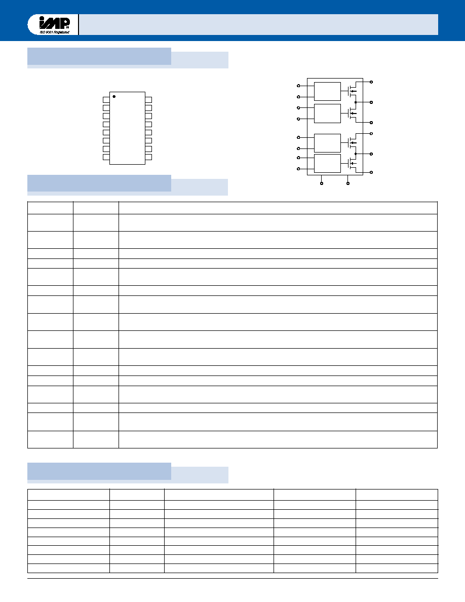
N 16-pin SO and DIP packages, Die available
N Pin compatible with the Micrel MIC2524 and
MIC2527
Typical Application
IMP252
IMP252
4/2
4/2
7
7
A
DVANCE
P
RODUCT
I
NFORMATION
P
OWER
M
ANAGEMENT
Quad USB High-Side P
Quad USB High-Side P
o
o
w
w
er
er
Switc
Switc
h wit
h wit
h F
h F
ault Det
ault Det
ection
ection
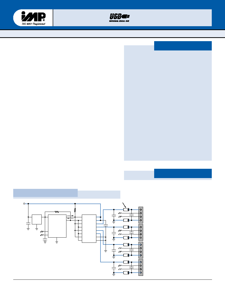
The IMP2524 and IMP2527 are complete power management solutions
for bus-powered and self-powered USB hubs. Each device contains four
independent power switches and fault detection logic. The IMP2524
channel resistance is a low 140m
maximum and the IMP2527 channel
resistance is 300
maximum. Both device operate with voltage inputs
from 2.7V to 5.5V
The IMP2524/2527 conform to the new USB 1.1 standard. Fault current
is limited to 750mA typically, and a flag output for each switch conveys
fault information to the local USB controller. The IMP252x "Soft-Start"
function ramps the ON-current to eliminate any excessive voltage drop
on the input side that could occur when capacitive loads are charged.
Self-monitoring features include thermal shutdown to prevent
catastrophic switch failure from high-current loads and undervoltage
lockout (UVLO) that insures that the device remains OFF unless there is
sufficient supply voltage present.
The switch Enable input logic can interface with both 3.3V and 5V logic.
Both active-HIGH (-1 devices) and active-LOW (-2 devices) enable logic
versions are available. Supply current is a low 0.75
µA when disabled and
just 110
µA when enabled
The quad IMP2524/7 devices are available in 16-pin DIP and 16-pin
SO packages and are pin compatible replacements for the Micrel
MIC2524-1/-2 and MIC2527-1/2 devices. IMP offers a complete family
of USB power management products. For single-switch applications see
the IMP2525 and IMP2525A data sheets. The single-switch IMP2525A
features a 0.07
switch resistance. For dual-switch applications, refer to
the IMP2526 data sheet.
Data
Ferrite Bead
2
1
3
4
5
6
7
8
INA/B
INC/D
OUTA
OUTB
OUTC
OUTD
GND
GND
16
15
14
13
12
11
10
9
ENA
FLGA
ENB
FLGB
ENC
FLGC
END
FLGD
IMP2524
IMP2527
USB Controller
V+
D+
D≠
ON/OFF
OVERCURRENT
LDO
OUT
IN
GND
GND
27k
1
mF
0.01
mF
0.1
mF
10k
2524/27_01.eps
33
mF*
GND
D≠
D+
Downstream
USB
Port 1
500mA max.
V
BUS
+
IMP2527
5.1V
± 3%
5V
± 1%
or
IMP2524
5V
± 3%
0.01
mF
33
mF*
GND
D≠
D+
Downstream
USB
Port 2
500mA max.
V
BUS
+
4.7
mF
+
0.01
mF
33
mF*
GND
D≠
D+
Downstream
USB
Port 3
500mA max.
V
BUS
+
0.01
mF
33
mF*
GND
D≠
D+
Downstream
USB
Port 4
500mA max.
V
BUS
+
Bold/
Blue
lines indicate 0.1" wide, 1-oz. copper high-current traces.
*33
mF, 16V tantalum or 100mF, 10V electrolytic per port
©
1999 IMP, Inc.
408-432-9100/www.impweb.com
3
IMP252
IMP252
4/2
4/2
7
7
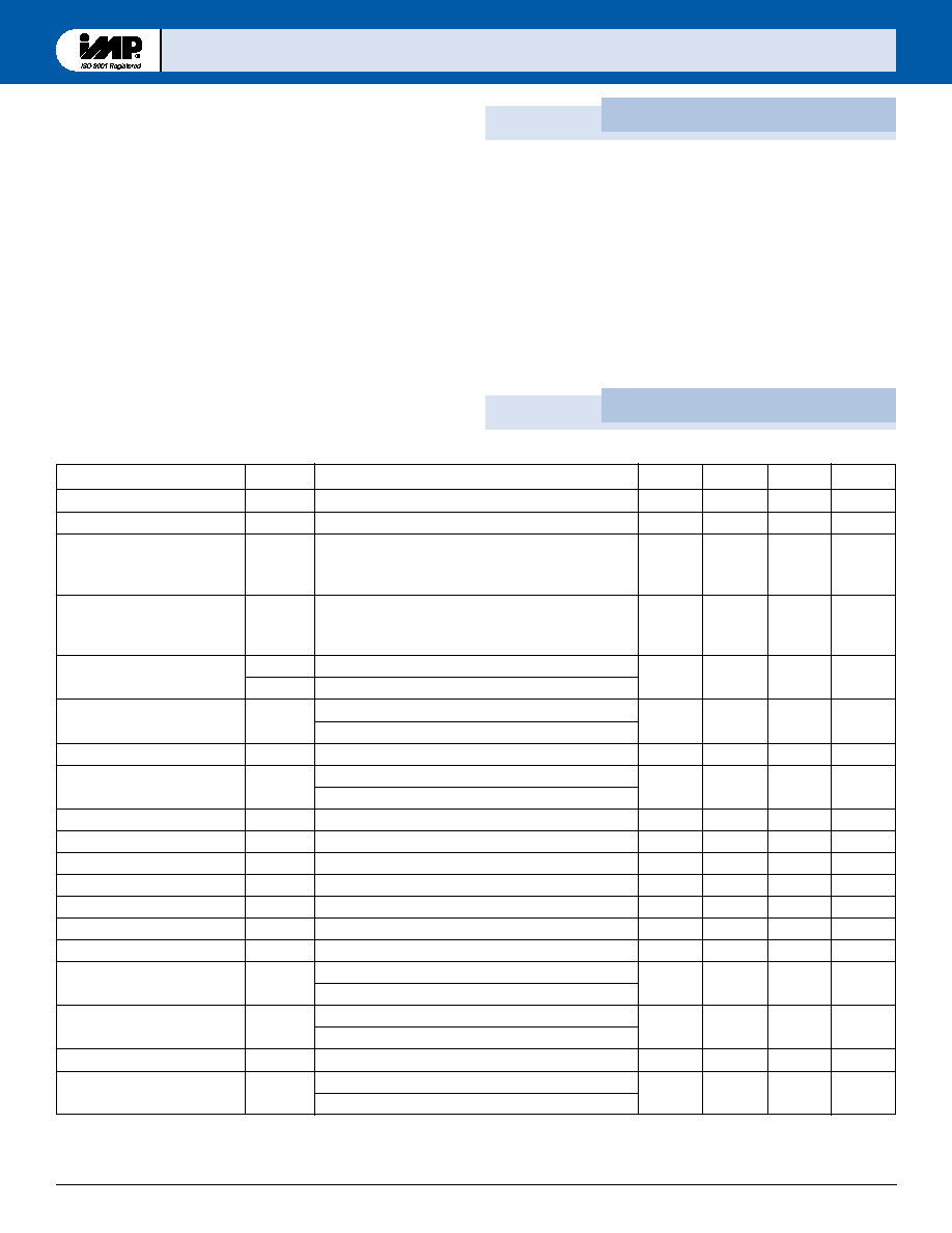
Absolute Maximum Ratings
Electrical Characteristics
Supply Voltage . . . . . . . . . . . . . . . . . . . . . . . . . . +8.0V
Fault Flag Voltage . . . . . . . . . . . . . . . . . . . . . . +8.0V
Fault Flag Current . . . . . . . . . . . . . . . . . . . . . . 50mA
Output Voltage . . . . . . . . . . . . . . . . . . . . . . . . . +8.0V
Output Current . . . . . . . . . . . . . . . . . . . . . . . . . Internally Limited
Enable Input . . . . . . . . . . . . . . . . . . . . . . . . . . . ≠0.3V to 12V
Storage Temperature . . . . . . . . . . . . . . . . . . . . . ≠65
∞C to +150∞C
Lead Temperature (Soldering, 5 sec.) . . . . . . . 260
∞C
Package Thermal Resistance
SO (
JA
) . . . . . . . . . . . . . . . . . . . . . . . . . . . . 160
∞C/W
DIP(
JA
) . . . . . . . . . . . . . . . . . . . . . . . . . . . . 130
∞C/W
Note: All voltages are referenced to GND.
These are stress ratings only and functional operation is not
implied. Exposure to absolute maximum ratings for prolonged
time periods may affect device reliability.
Parameter
Symbol Conditions
Min
Typ
Max
Units
Supply Voltage Range
V
IN
T
A
= ≠ 40
∞C to +85∞C
2.7
5.5
V
Operating Temperature Range
T
A
≠ 40
85
∞C
Supply Current
I
IN OFF
Switch OFF, No load
0.75
10
µA
Switch OFF
V
ENOFF
0.8V, V
ENON
2.4V IMP2524/27-1
V
ENON
0.8V, V
ENOFF
2.4V IMP2524/27-2
Supply Current
I
IN ON
Switch ON, No load
110
320
µA
Switch ON
V
ENOFF
0.8V, V
ENON
2.4V IMP2524/27-1
V
ENON
0.8V, V
ENOFF
2.4V IMP2524/27-2
Enable Input Threshold
V
ENH
LOW to HIGH ("0" to "1") Enable Voltage, Note 1
2.1
2.4
V
V
ENL
HIGH to LOW ("1" to "0") Enable Voltage, Note 1
0.8
1.9
Enable Input Current
I
EN
V
EN
= 2.4V
0.01
1
µA
V
EN
= 0.8V
0.01
1
Enable Input Capacitance
C
EN
1
pF
Switch ON Resistance
R
ON
IMP2524: I
OUT
= 500mA each switch
0.10
0.14
IMP2527: I
OUT
= 500mA each switch
0.20
0.30
Continuous Load Current
I
L
Each output
0.5
A
Output Turn-On Delay
T
DON
R
L
= 10
each output
0.25
ms
Output Turn-On Rise Time
T
RON
R
L
= 10
each output
1
ms
Output Turn-Off Delay
T
DOFF
R
L
= 10
each output
1
20
µs
Output Turn-Off Fall Time
T
FOFF
R
L
= 10
each output
1
20
µs
Output Leakage Current
I
OFF
10
µA
Short-circuit Current Limit
I
SC
0.50
0.75
1.25
A
Overtemperature Shutdown
T
J
increasing
135
∞C
Threshold T
J
decreasing 125
Error Flag Output Resistance
R
FLAG
V
IN
= 5V, I
L
= 10mA
10
V
IN
= 3.3V, I
L
= 10mA
15
Error Flag Output Current
I
FLAG
V
FLAG
= 5V
0.01
1
µA
UVLO Threshold
V
UVLO
V
IN
Increasing
2.5
V
V
IN
Decreasing
2.3
Unless otherwise noted, V
IN
= 5V and T
A
= 25∞C.
Notes 1. Switch OFF is V
EN
0.8V and Switch ON is V
EN
2.4V for the IMP2524/27-1. Switch OFF is V
EN
2.4V and Switch ON is
V
EN
0.8V for the IMP2524/27-2. The Enable input has approximately 200mV of hysteresis.
IMP252
IMP252
4/2
4/2
7
7
IMP, Inc.
Corporate Headquarters
2830 N. First Street
San Jose, CA 95134-2071
Tel: 408-432-9100
Tel: 800-438-3722
Fax: 408-434-0335
e-mail: info@impinc.com
http://www.impweb.com
The IMP logo is a registered trademark of IMP, Inc.
All other company and product names are trademarks of their respective owners.
© 1999 IMP, Inc.
Printed in USA
Publication #: 5005
Revision:
B
Issue Date:
05/17/00
Type:
Preliminary
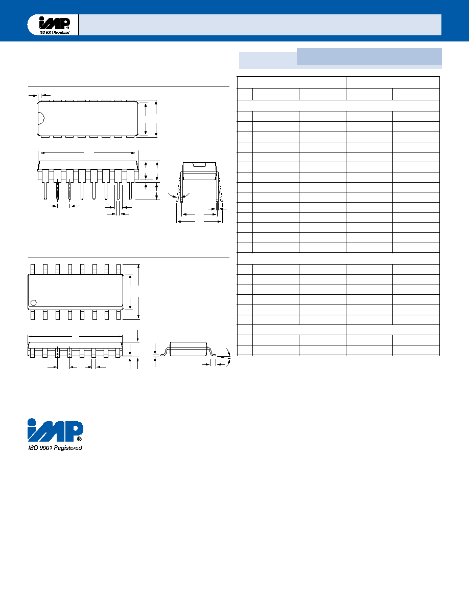
D1
N
D
E
eA
eB
E1
C
0
∞≠15∞
A
e
B1
B
A2
L
A1
Plastic DIP (16-Pin).eps
Plastic DIP (16-Pin)
H
E
e
B
D
A1
A
L
0
∞≠ 8∞
C
16-Pin (SO).eps
SO (16-Pin)
Package Dimensions
s
e
h
c
n
I
s
r
e
t
e
m
i
ll
i
M
n
i
M
x
a
M
n
i
M
x
a
M
*
)
n
i
P
-
6
1
(
P
I
D
c
i
t
s
a
l
P
A
--
--
--
0
0
2
.
0
--
--
--
8
0
.
5
1
A
5
1
0
.
0
--
--
--
8
3
.
0
--
--
--
2
A
5
2
1
.
0
5
7
1
.
0
8
1
.
3
5
4
.
4
B
6
1
0
.
0
2
2
0
.
0
1
4
.
0
6
5
.
0
1
B
5
4
0
.
0
5
6
0
.
0
4
1
.
1
5
6
.
1
C
8
0
0
.
0
2
1
0
.
0
0
2
.
0
0
3
.
0
D
5
4
7
.
0
5
6
7
.
0
2
9
.
8
1
3
4
.
9
1
1
D
5
0
0
.
0
0
8
0
.
0
3
1
.
0
3
0
.
2
E
0
0
3
.
0
5
2
3
.
0
2
6
.
7
6
2
.
8
1
E
0
4
2
.
0
0
1
3
.
0
0
1
.
6
7
8
.
7
e
0
0
1
.
0
--
--
--
4
5
.
2
--
--
--
A
e
0
0
3
.
0
--
--
--
2
6
.
7
--
--
--
B
e
--
--
--
0
0
4
.
0
--
--
--
6
1
.
0
1
L
5
1
1
.
0
0
5
1
.
0
2
9
.
2
1
8
.
3
*
*
)
n
i
P
-
6
1
(
O
S
A
6
2
9
.
0
3
4
0
1
.
0
5
3
.
2
5
6
.
2
1
A
0
4
0
0
.
0
8
1
1
0
.
0
0
1
.
0
0
3
.
0
B
3
1
0
.
0
0
2
0
.
0
3
3
.
0
1
5
.
0
C
1
9
0
0
.
0
5
2
1
0
.
0
3
2
.
0
2
3
.
0
D
7
7
9
3
.
0
3
3
1
4
.
0
0
1
.
0
1
0
5
.
0
1
E
4
1
9
2
.
0
2
6
6
2
.
0
0
4
.
7
0
6
.
7
e
C
S
B
0
5
0
.
0
C
S
B
7
2
.
1
H
4
9
3
.
0
9
1
4
.
0
0
0
.
0
1
5
6
.
0
1
L
6
1
0
.
0
0
5
0
.
0
0
4
.
0
7
2
.
1
B
A
8
5
0
-
O
M
g
n
i
w
a
r
D
C
E
D
E
J
*
A
A
3
1
0
-
S
M
g
n
i
w
a
r
D
C
E
D
E
J
*
*
3
t
a
.
3
0
t
_
6
2
/
4
2
5
2