© 2000 IMP, Inc.
408-432-9100/www.impweb.com
1
IMP38C/HC/42/3/4/5
IMP38C/HC/42/3/4/5
P
OWER
M
ANAGEMENT
Key Features
N 384x Series Pinout with BiCMOS Technology
N Zero Cross-Conduction Current by Design
N 1MHz Operation
N 65ns Maximum Current-Sense Delay
N 120µA Maximum Start-Up Current
N 1.5mA Maximum Operating Current
N High Output Current Drive
≠ 1.0A, IMP38HC4x
≠ 0.5A, IMP38C4x
N 20V Maximum Supply Voltage
N 2.5V, 1%, Trimmed Error Amplifier Reference
N Trimmed Oscillator Discharge Current
N Pin-for-Pin Enhanced Replacements for Micrel
MIC38C/HC4x and GMT38C4x/HC4x
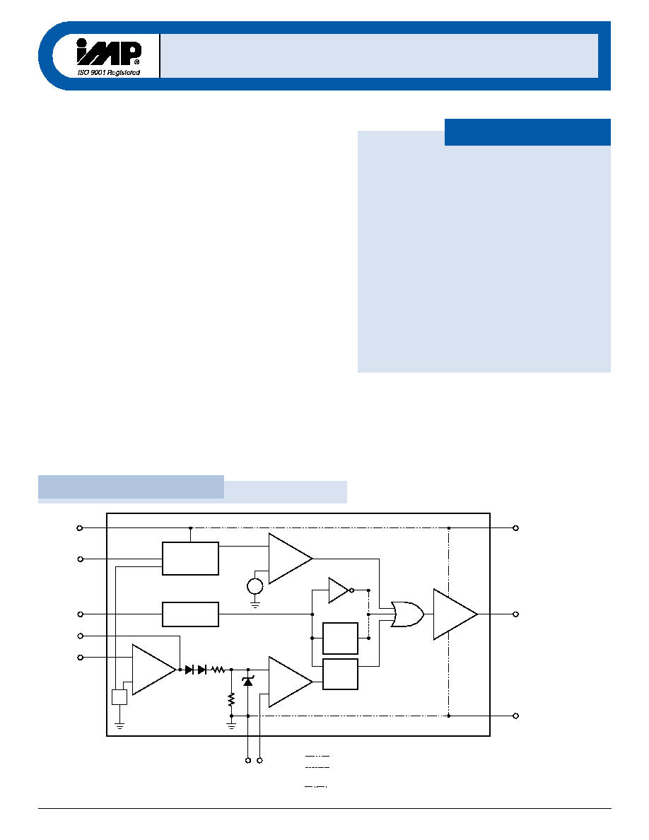
Block Diagrams
BiCMOS Cur
BiCMOS Cur
r
r
ent-Mode
ent-Mode
PWM Contr
PWM Contr
oller
oller
s
s
≠
≠
1MHz Oper
1MHz Oper
ation
ation
≠
≠
N
N
o Cr
o Cr
os
os
s
s
-
-
Conduction Cur
Conduction Cur
r
r
ent
ent
≠
≠
50ns Cur
50ns Cur
r
r
ent-Sense Dela
ent-Sense Dela
y
y
The IMP38C4x and IMP38HC4x are fixed frequency, high performance,
current-mode PWM controllers that are pin compatible with bipolar 384x
devices but feature improvements resulting from IMP's BiCMOS
processing and circuit design. Notable among the improvements are zero
cross-conduction/shoot-through current, reduced start-up and operating
current, lower current-sense delay, higher frequency operation, full
supply voltage swing at the output and a 1% trimmed voltage reference.
IMP38C4x and IMP38HC4x output driver stage has zero cross-conduction
current. A proprietary output state-machine monitors each output
MOSFET and guarantees by design zero cross-conduction current. This is
an industry first for 384x PWM devices.
Under-voltage lockout (UVL) performance has been improved. When
the power supply voltage is below the startup voltage, internal circuitry
puts the output into a low impedance state. The output will sink 20mA
and remain below 1.3V, well below the turn-on threshold voltage of the
external MOSFET. Even when V
DD
drops to zero volts, the out pin will
not rise above approximately 1.3V because the output UVLO circuit is
+
≠
EA
OUT
6 (10)
RTCT
4 (7)
COMP
1 (1)
V
DD
V
REF
5V
Reference
7 (12)
8 (14)
FB
2 (3)
V
D
(11)
≠
+
+
≠
UVLO
+
≠
COMP
PGND
(8)
Oscillator
T
Q
S
Q
R
1V
R
2R
2.5V
Ref
( ) Pins Are 14-Pin Devices Only
38C/HC_01.eps
+
≠
GND 5
AGND (9)
3 (5)
ISNS
Connection Notes
IMP38C4X, IMP38HC4X (8-Pin Devices)
50% Maximum Duty Cycle:
IMP38C44, IMP38HC44, IMP38C45, IMP38HC45
96% Maximum Duty Cycle:
IMP38C42, IMP38HC42, IMP38C43, IMP38HC43
I M P 3 8 C / H C / 4 2 / 3 / 4 / 5
I M P 3 8 C / H C / 4 2 / 3 / 4 / 5
2
408-432-9100/www.impweb.com
© 2000 IMP, Inc.
!S
Pin Descriptions
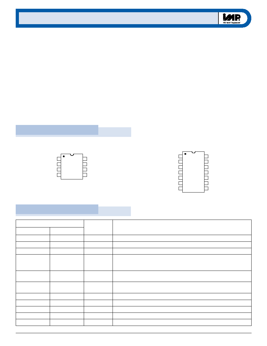
Pin Configuration
IMP38C4x
IMP38HC4x
1
COMP
2
FB
3
ISNS
4
RT/CT
V
REF
V
DD
OUT
GND
8
7
6
5
38C/HC_02.eps
SO/MicroSO/DIP
SO/DIP
IMP38C4x
IMP38HC4x
1
COMP
2
NC
3
FB
4
NC
V
REF
NC
V
DD
V
D
14
13
12
11
5
ISNS
OUT
10
6
NC
AGND
9
7
RT/CT
PGND
8
38C/HC_03.eps
r
e
b
m
u
N
n
i
P
e
m
a
N
n
o
i
t
c
n
u
F
e
g
a
k
c
a
P
n
i
P
-
8
e
g
a
k
c
a
P
n
i
P
-
4
1
1
1
P
M
O
C
.
r
o
t
a
r
a
p
m
o
c
M
W
P
e
h
t
o
t
t
u
p
n
i
d
n
a
r
e
i
f
il
p
m
a
r
o
r
r
E
e
h
t
f
o
t
u
p
t
u
O
2
3
B
F
.
r
e
i
f
il
p
m
A
r
o
r
r
E
e
h
t
f
o
t
u
p
n
i
g
n
i
t
r
e
v
n
I
3
5
S
N
S
I
.
V
1
o
t
d
e
t
i
m
il
y
ll
a
n
r
e
t
n
i
s
i
t
I
.
t
u
p
n
i
r
o
t
a
r
a
p
m
o
c
e
s
n
e
s
t
n
e
r
r
u
C
4
7
T
C
/
T
R
o
t
d
e
t
c
e
n
n
o
c
s
i
T
R
r
o
t
s
i
s
e
R
.
n
o
i
t
c
e
n
n
o
c
t
n
e
n
o
p
m
o
c
g
n
i
m
i
t
C
R
r
o
t
a
ll
i
c
s
O
V
F
E
R
d
n
a
T
R
f
o
s
e
u
l
a
v
t
n
e
r
e
f
f
i
D
.
d
n
u
o
r
g
o
t
d
e
t
c
e
n
n
o
c
s
i
T
C
r
o
t
i
c
a
p
a
c
d
n
a
.
e
l
c
y
c
y
t
u
d
m
u
m
i
x
a
m
e
h
t
e
n
i
m
r
e
t
e
d
T
C
5
8
D
N
G
P
/
D
N
G
r
e
w
o
p
d
n
a
s
e
c
i
v
e
d
d
e
g
a
k
c
a
p
n
i
p
-
8
r
o
f
d
n
u
o
r
g
g
o
l
a
n
a
d
n
a
r
e
w
o
p
d
e
n
i
b
m
o
C
.
e
g
a
k
c
a
p
n
i
p
-
4
1
r
o
f
d
n
u
o
r
g
6
0
1
T
U
O
n
e
h
w
W
O
L
d
l
e
h
y
l
e
v
i
t
c
a
s
i
n
i
p
T
U
O
.
t
u
p
t
u
o
r
e
v
i
r
d
e
l
o
p
-
m
e
t
o
t
,
r
e
w
o
p
-
h
g
i
H
V
C
C
.
d
l
o
h
s
e
r
h
t
O
L
V
U
e
h
t
w
o
l
e
b
s
i
7
2
1
V
D
D
.
t
u
p
n
i
e
g
a
t
l
o
v
y
l
p
p
u
S
8
4
1
V
F
E
R
.
t
u
p
t
u
o
e
g
a
t
l
o
v
e
c
n
e
r
e
f
e
r
-
V
5
9
D
N
G
A
.
e
g
a
k
c
a
p
n
i
p
-
4
1
r
o
f
n
o
i
t
c
e
n
n
o
c
d
n
u
o
r
g
g
o
l
a
n
A
1
1
V
D
.
e
g
a
k
c
a
p
n
i
p
-
4
1
r
o
f
e
g
a
t
l
o
v
y
l
p
p
u
s
r
e
v
i
r
d
t
u
p
t
u
O
3
1
,
6
,
4
,
2
C
N
.
n
o
i
t
c
e
n
n
o
c
l
a
n
r
e
t
n
i
o
N
s
p
e
.
1
0
t
_
C
H
-
C
8
3
powered through the out pin. Leakage current from the external
power MOSFETs will not force the PWM output to rise and turn
the external MOSFETs on.
Current-sense propagation delay time is 35ns typical, 65ns maxi-
mum, representing an up to 75 percent reduction over other 38xx
implementations.
Output stage drive is 0.5A for IMP38C4x devices. The high-drive
IMP38HC4x family is rated at 1.0A peak current drive.
Like conventional 384x controllers, the IMP38C4x and
IMP38HC4x controllers use the current-mode architecture for
superior load regulation, pulse-by-pulse current limiting and out-
put MOSFET protection. All versions operate up to 20 volts.
For maximum application flexibility, start-up voltage ranges from
14.5V to 8.4V. Start-up current has been reduced to 120
µA maxi-
mum and operating current has been reduced to 1.5mA maximum.
The IMP38C4x/IMP38HC4x are available in 8-pin and 14-pin DIP
and SO packages as well as the 8-pin MicroSO package. The 14-
pin devices provide separate pins for the controller power supply
and the output driver supply. This configuration maximizes
application flexibility and performance. The 14-pin package can
also dissipate more power. Devices in the compact 8-pin packages
do not have separate output drive supply connections.
The IMP38C4x and IMP38HC4x families operate over the ≠40
∞C
to +85
∞C temperature range.
I M P 3 8 C / H C / 4 2 / 3 / 4 / 5
I M P 3 8 C / H C / 4 2 / 3 / 4 / 5
© 2000 IMP, Inc.
PWM Controllers
3
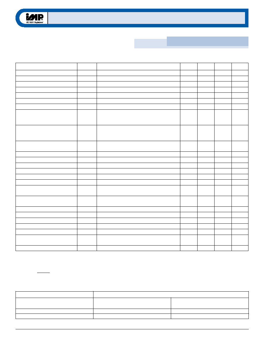
Ordering Information
g
n
i
r
e
d
r
O
P
M
I
r
e
b
m
u
N
t
r
a
P
e
g
a
k
c
a
P
g
n
i
t
a
r
e
p
O
e
r
u
t
a
r
e
p
m
e
T
e
g
n
a
R
p
u
t
r
a
t
S
e
g
a
t
l
o
V
m
u
m
i
n
i
M
g
n
i
t
a
r
e
p
O
e
g
a
t
l
o
V
m
u
m
i
x
a
M
e
l
c
y
C
y
t
u
D
e
c
n
e
r
e
f
e
R
e
g
a
t
l
o
V
t
u
p
t
u
O
k
a
e
P
e
v
i
r
D
t
n
e
r
r
u
C
A
P
E
2
4
C
8
3
P
M
I
P
I
D
c
i
t
s
a
l
P
-
8
≠ 0
4 ∞
5
8
o
t
C
∞C
V
5
.
4
1
V
0
.
9
%
6
9
V
5
.
2
A
5
.
0
D
P
E
2
4
C
8
3
P
M
I
P
I
D
c
i
t
s
a
l
P
-
4
1
≠ 0
4 ∞
5
8
o
t
C
∞C
V
5
.
4
1
V
0
.
9
%
6
9
V
5
.
2
A
5
.
0
A
S
E
2
4
C
8
3
P
M
I
O
S
-
8
≠ 0
4 ∞
5
8
o
t
C
∞C
V
5
.
4
1
V
0
.
9
%
6
9
V
5
.
2
A
5
.
0
D
S
E
2
4
C
8
3
P
M
I
O
S
-
4
1
≠ 0
4 ∞
5
8
o
t
C
∞C
V
5
.
4
1
V
0
.
9
%
6
9
V
5
.
2
A
5
.
0
A
M
E
2
4
C
8
3
P
M
I
O
S
o
r
c
i
M
-
8
≠ 0
4 ∞
5
8
o
t
C
∞C
V
5
.
4
1
V
0
.
9
%
6
9
V
5
.
2
A
5
.
0
D
/
2
4
C
8
3
P
M
I
E
I
D
A
P
E
3
4
C
8
3
P
M
I
P
I
D
c
i
t
s
a
l
P
-
8
≠ 0
4 ∞
5
8
o
t
C
∞C
V
4
.
8
V
6
.
7
%
6
9
V
5
.
2
A
5
.
0
D
P
E
3
4
C
8
3
P
M
I
P
I
D
c
i
t
s
a
l
P
-
4
1
≠ 0
4 ∞
5
8
o
t
C
∞C
V
4
.
8
V
6
.
7
%
6
9
V
5
.
2
A
5
.
0
A
S
E
3
4
C
8
3
P
M
I
O
S
-
8
≠ 0
4 ∞
5
8
o
t
C
∞C
V
4
.
8
V
6
.
7
%
6
9
V
5
.
2
A
5
.
0
D
S
E
3
4
C
8
3
P
M
I
O
S
-
4
1
≠ 0
4 ∞
5
8
o
t
C
∞C
V
4
.
8
V
6
.
7
%
6
9
V
5
.
2
A
5
.
0
A
M
E
3
4
C
8
3
P
M
I
O
S
o
r
c
i
M
-
8
≠ 0
4 ∞
5
8
o
t
C
∞C
V
4
.
8
V
6
.
7
%
6
9
V
5
.
2
A
5
.
0
D
/
3
4
C
8
3
P
M
I
E
I
D
A
P
E
4
4
C
8
3
P
M
I
P
I
D
c
i
t
s
a
l
P
-
8
≠ 0
4 ∞
5
8
o
t
C
∞C
V
5
.
4
1
V
0
.
9
%
0
5
V
5
.
2
A
5
.
0
D
P
E
4
4
C
8
3
P
M
I
P
I
D
c
i
t
s
a
l
P
-
4
1
≠ 0
4 ∞
5
8
o
t
C
∞C
V
5
.
4
1
V
0
.
9
%
0
5
V
5
.
2
A
5
.
0
A
S
E
4
4
C
8
3
P
M
I
O
S
-
8
≠ 0
4 ∞
5
8
o
t
C
∞C
V
5
.
4
1
V
0
.
9
%
0
5
V
5
.
2
A
5
.
0
D
S
E
4
4
C
8
3
P
M
I
O
S
-
4
1
≠ 0
4 ∞
5
8
o
t
C
∞C
V
5
.
4
1
V
0
.
9
%
0
5
V
5
.
2
A
5
.
0
A
M
E
4
4
C
8
3
P
M
I
O
S
o
r
c
i
M
-
8
≠ 0
4 ∞
5
8
o
t
C
∞C
V
5
.
4
1
V
0
.
9
%
0
5
V
5
.
2
A
5
.
0
D
/
4
4
C
8
3
P
M
I
E
I
D
A
P
E
5
4
C
8
3
P
M
I
P
I
D
c
i
t
s
a
l
P
-
8
≠ 0
4 ∞
5
8
o
t
C
∞C
V
4
.
8
V
6
.
7
%
0
5
V
5
.
2
A
5
.
0
D
P
E
5
4
C
8
3
P
M
I
P
I
D
c
i
t
s
a
l
P
-
4
1
≠ 0
4 ∞
5
8
o
t
C
∞C
V
4
.
8
V
6
.
7
%
0
5
V
5
.
2
A
5
.
0
A
S
E
5
4
C
8
3
P
M
I
O
S
-
8
≠ 0
4 ∞
5
8
o
t
C
∞C
V
4
.
8
V
6
.
7
%
0
5
V
5
.
2
A
5
.
0
D
S
E
5
4
C
8
3
P
M
I
O
S
-
4
1
≠ 0
4 ∞
5
8
o
t
C
∞C
V
4
.
8
V
6
.
7
%
0
5
V
5
.
2
A
5
.
0
A
M
E
5
4
C
8
3
P
M
I
O
S
o
r
c
i
M
-
8
≠ 0
4 ∞
5
8
o
t
C
∞C
V
4
.
8
V
6
.
7
%
0
5
V
5
.
2
A
5
.
0
D
/
5
4
C
8
3
P
M
I
E
I
D
A
P
E
2
4
C
H
8
3
P
M
I
P
I
D
c
i
t
s
a
l
P
-
8
≠ 0
4 ∞
5
8
o
t
C
∞C
V
5
.
4
1
V
0
.
9
%
6
9
V
5
.
2
A
0
.
1
D
P
E
2
4
C
H
8
3
P
M
I
P
I
D
c
i
t
s
a
l
P
-
4
1
≠ 0
4 ∞
5
8
o
t
C
∞C
V
5
.
4
1
V
0
.
9
%
6
9
V
5
.
2
A
0
.
1
A
S
E
2
4
C
H
8
3
P
M
I
O
S
-
8
≠ 0
4 ∞
5
8
o
t
C
∞C
V
5
.
4
1
V
0
.
9
%
6
9
V
5
.
2
A
0
.
1
D
S
E
2
4
C
H
8
3
P
M
I
O
S
-
4
1
≠ 0
4 ∞
5
8
o
t
C
∞C
V
5
.
4
1
V
0
.
9
%
6
9
V
5
.
2
A
0
.
1
A
M
E
2
4
C
H
8
3
P
M
I
O
S
o
r
c
i
M
-
8
≠ 0
4 ∞
5
8
o
t
C
∞C
V
5
.
4
1
V
0
.
9
%
6
9
V
5
.
2
A
0
.
1
D
/
2
4
C
H
8
3
P
M
I
E
I
D
A
P
E
3
4
C
H
8
3
P
M
I
P
I
D
c
i
t
s
a
l
P
-
8
≠ 0
4 ∞
5
8
o
t
C
∞C
V
4
.
8
V
6
.
7
%
6
9
V
5
.
2
A
0
.
1
D
P
E
3
4
C
H
8
3
P
M
I
P
I
D
c
i
t
s
a
l
P
-
4
1
≠ 0
4 ∞
5
8
o
t
C
∞C
V
4
.
8
V
6
.
7
%
6
9
V
5
.
2
A
0
.
1
A
S
E
3
4
C
H
8
3
P
M
I
O
S
-
8
≠ 0
4 ∞
5
8
o
t
C
∞C
V
4
.
8
V
6
.
7
%
6
9
V
5
.
2
A
0
.
1
D
S
E
3
4
C
H
8
3
P
M
I
O
S
-
4
1
≠ 0
4 ∞
5
8
o
t
C
∞C
V
4
.
8
V
6
.
7
%
6
9
V
5
.
2
A
0
.
1
A
M
E
3
4
C
H
8
3
P
M
I
O
S
o
r
c
i
M
-
8
≠ 0
4 ∞
5
8
o
t
C
∞C
V
4
.
8
V
6
.
7
%
6
9
V
5
.
2
A
0
.
1
D
/
3
4
C
H
8
3
P
M
I
E
I
D
A
P
E
4
4
C
H
8
3
P
M
I
P
I
D
c
i
t
s
a
l
P
-
8
≠ 0
4 ∞
5
8
o
t
C
∞C
V
5
.
4
1
V
0
.
9
%
0
5
V
5
.
2
A
0
.
1
D
P
E
4
4
C
H
8
3
P
M
I
P
I
D
c
i
t
s
a
l
P
-
4
1
≠ 0
4 ∞
5
8
o
t
C
∞C
V
5
.
4
1
V
0
.
9
%
0
5
V
5
.
2
A
0
.
1
A
S
E
4
4
C
H
8
3
P
M
I
O
S
-
8
≠ 0
4 ∞
5
8
o
t
C
∞C
V
5
.
4
1
V
0
.
9
%
0
5
V
5
.
2
A
0
.
1
D
S
E
4
4
C
H
8
3
P
M
I
O
S
-
4
1
≠ 0
4 ∞
5
8
o
t
C
∞C
V
5
.
4
1
V
0
.
9
%
0
5
V
5
.
2
A
0
.
1
A
M
E
4
4
C
H
8
3
P
M
I
O
S
o
r
c
i
M
-
8
≠ 0
4 ∞
5
8
o
t
C
∞C
V
5
.
4
1
V
0
.
9
%
0
5
V
5
.
2
A
0
.
1
D
/
4
4
C
H
8
3
P
M
I
E
I
D
A
P
E
5
4
C
H
8
3
P
M
I
P
I
D
c
i
t
s
a
l
P
-
8
≠ 0
4 ∞
5
8
o
t
C
∞C
V
4
.
8
V
6
.
7
%
0
5
V
5
.
2
A
0
.
1
D
P
E
5
4
C
H
8
3
P
M
I
P
I
D
c
i
t
s
a
l
P
-
4
1
≠ 0
4 ∞
5
8
o
t
C
∞C
V
4
.
8
V
6
.
7
%
0
5
V
5
.
2
A
0
.
1
A
S
E
5
4
C
H
8
3
P
M
I
O
S
-
8
≠ 0
4 ∞
5
8
o
t
C
∞C
V
4
.
8
V
6
.
7
%
0
5
V
5
.
2
A
0
.
1
D
S
E
5
4
C
H
8
3
P
M
I
O
S
-
4
1
≠ 0
4 ∞
5
8
o
t
C
∞C
V
4
.
8
V
6
.
7
%
0
5
V
5
.
2
A
0
.
1
A
M
E
5
4
C
H
8
3
P
M
I
O
S
o
r
c
i
M
-
8
≠ 0
4 ∞
5
8
o
t
C
∞C
V
4
.
8
V
6
.
7
%
0
5
V
5
.
2
A
0
.
1
D
/
5
4
C
H
8
3
P
M
I
E
I
D
s
p
e
.
2
0
t
_
C
H
/
C
8
3
For SO and MicroSO packages, append "/T" to the ordering part number for tape and reel packaging.
I M P 3 8 C / H C / 4 2 / 3 / 4 / 5
I M P 3 8 C / H C / 4 2 / 3 / 4 / 5
4
408-432-9100/www.impweb.com
© 2000 IMP, Inc.
!S
Absolute Maximum Ratings
V
CC
Supply Voltage . . . . . . . . . . . . . . . . . . . . . . 20V
V
CC
Supply Current . . . . . . . . . . . . . . . . . . . . . . 30mA
I
OUT
Current . . . . . . . . . . . . . . . . . . . . . . . . . . . . 1.0A
Current-Sense and Feedback Inputs . . . . . . . . 0.3V to 5.5V
Operation Junction Temperature . . . . . . . . . . . +150
∞C
Storage Temperature . . . . . . . . . . . . . . . . . . . . . ≠ 65
∞C to +150∞C
Lead Soldering Temperature (10 seconds) . . . +300
∞C
Parameter
Symbol
Conditions
Min
Typ
Max
Units
Reference
Output voltage
V
REF
T
A
= +25
∞C, I
O
= 1mA
4.90
5.00
5.10
V
Line Regulation
12V
V
CC
18V, I
OUT
= 5
µA
2
20
mV
Load Regulation
1mA
I
O
20mA
1
25
mV
Temperature Stability
TC
REF
Note 1
0.2
mV/
∞C
Total Reference Variation
Line, Load, Temperature, Note 1
4.82
5.18
V
Output Noise Voltage
V
N
10Hz
f 10kHz, T
A
= +25
∞C, Note 1
50
µV
Long Term Stability
T
A
= 125
∞C, 1000 Hours, Note 1
TBD
mV
Output Short Circuit
I
SC
≠ 30
≠ 40
≠ 180
mA
Oscillator Section
Initial Accuracy
f
INIT
T
A
= 25
∞C, Note 5
49
52
55
kHz
Voltage Stability
12V
V
CC
18V
0.2
1.0
%
Temperature Stability
TC
OSC
Note 1
0.04
%/
∞C
Discharge Current
V
RT/CT
= 2V
7.2
8.4
12.0
mA
Amplitude peak-to-peak
V
OSC, P-P
V
RT/CT
peak-to-peak
1.1
1.7
2.3
V
Error Amplifier Section
Input Voltage
V
IN
V
COMP
= 2.5V
2.45
2.50
2.55
V
Input Bias Current
I
B
V
FB
= 4.5V
≠1
1
µA
Open Loop Gain
A
VOL
2V
V
O
4V, Note 1
65
90
dB
Unity Gain Bandwidth
UGBW
Note1
0.7
1.0
MHz
Power Supply Rejection Ratio
PSRR
V
START
V
CC
V
CCMAX
60
dB
Output Sink Current
I
OL
V
FB
= 2.7V, Vcomp = 1.1V
2
6
mA
Output Source Current
I
OH
V
FB
= 2.3V, Vcomp = 5.0V
≠ 0.5
≠ 1.0
mA
V
OUT
High
V
OH
V
FB
= 2.3V, R
L
= 15k
to ground
4.5
4.6
5.0
V
V
OUT
Low
V
OL
V
FB
= 2.7V, R
L
= 15k
to V
REF
0.30
0.50
V
Unless otherwise noted, V
CC
= 15V, RT = 10k
and CT = 3.3nF. Specifications are over the ≠ 40∞C to +85∞C ambient temperature range.
Bold/
blue
specifications indicate enhanced performance features.
Electrical Characteristics
Package Thermal Resistance
8-Pin Plastic DIP (
JA
) . . . . . . . . . . . . . . . . . 125
∞C/W
8-Pin MicroSO (
JA
) . . . . . . . . . . . . . . . . . . . 250
∞C/W
8-Pin SO (
JA
) . . . . . . . . . . . . . . . . . . . . . . . . 170
∞C/W
14-Pin Plastic DIP (
JA
) . . . . . . . . . . . . . . . . 90
∞C/W
14-Pin SO (
JA
) . . . . . . . . . . . . . . . . . . . . . . . 145
∞C/W
Note: All voltages are referenced to GND.
These are stress ratings only and functional operation is not
implied. Exposure to absolute maximum ratings for prolonged
time periods may affect device reliability.
I M P 3 8 C / H C / 4 2 / 3 / 4 / 5
I M P 3 8 C / H C / 4 2 / 3 / 4 / 5
© 2000 IMP, Inc.
PWM Controllers
5
Electrical Characteristics
Parameter
Symbol
Conditions
Min
Typ
Max
Units
Current Sense
Gain
A
VOL
Notes 1, 2 and 3
2.90
3.00
3.10
V/V
Over Current Protection Threshold
Vcomp = max, Note 2
0.9
0.98
1.1
V
Power Supply Rejection Ratio
PSRR
V
START
V
CC
18V
70
dB
Input Bias Current
I
B
≠ 0.1
≠ 2.0
µA
Delay to Output
T
PD
V
FB
= 0V, ISNS 0V to 2V, C
L
= 1nF
50
65
ns
Output
IMP38C4x
ON Resistance, High
R
DS (ON)
I
SOURCE
= 0.2A
20
ON Resistance, Low
I
SINK
= 0.2A
11
IMP38HC4x
ON Resistance, High
R
DS (ON)
I
SOURCE
= 0.2A
10
ON Resistance, Low
I
SINK
= 0.2A
5.5
Peak Drive Current
HC devices
1.0
A
H devices
0.5
IMP38C4x Rise Time
T
R
T
A
= 25
∞C, C
L
= 1nF
40
70
ns
IMP38C4x Fall Time
T
F
T
A
= 25
∞C, C
L
= 1nF
30
50
ns
IMP38HC4x Rise Time
T
R
T
A
= 25
∞C, C
L
= 1nF
20
50
ns
IMP38HC4x Fall Time
T
F
T
A
= 25
∞C, C
L
= 1nF
15
40
ns
Shoot-through Current
0
mA
Undervoltage Lockout
Start Threshold
IMP38C42/4, IMP38HC42/4
13.5
14.5
15.5
V
IMP38C43/5, IMP38HC43/5
7.8
8.4
9.0
Minimum Operating Voltage
IMP38C42/4, IMP38HC42/4
8
9
10
V
IMP38C43/5, IMP38HC43/5
7.0
7.6
8.2
Pulse Width Modulator
Maximum Duty Cycle
IMP38C42/3, IMP38HC42/3,
94
96
%
Maximum Duty Cycle
IMP38C44/5, IMP38HC44/5
48
50
%
Minimum Duty Cycle
0
%
Supply Current
Start-Up Current
V
CC
= 13V for IMP38C42/44, IMP38HC42/44
95
120
µA
V
CC
= 7.5V for IMP38C43/45, IMP38HC43/45
Operating Current
I
CC
V
FB
= V
IS
= 0
0.5
1.5
mA
Unless otherwise noted, V
CC
= 15V, R
T
= 10k
and C
T
= 3.3nF. Specifications are over the ≠ 40∞C to +85∞C ambient temperature range.
Bold/
blue
specifications indicate enhanced performance features.
Note 1. Guaranteed by design. Not 100% tested in production.
Note 2. Measured at trip point of V
FB
= 0V.
Note 3. Gain is defined as:
s
d
l
o
h
s
e
r
h
T
O
L
V
U
e
l
c
y
C
y
t
u
D
V
4
.
8
t
a
p
u
-t
r
a
t
S
V
6
.
7
=
m
u
m
i
n
i
M
g
n
i
t
a
r
e
p
O
V
5
.
4
1
t
a
p
u
-t
r
a
t
S
V
0
.
9
=
m
u
m
i
n
i
M
g
n
i
t
a
r
e
p
O
%
6
9
o
t
%
0
3
4
C
H
/
3
4
C
8
3
P
M
I
2
4
C
H
/
2
4
C
8
3
P
M
I
%
0
5
o
t
%
0
5
4
C
H
/
5
4
C
8
3
P
M
I
4
4
C
H
/
4
4
C
8
3
P
M
I
s
p
e
.
3
0
t
_
C
H
/
C
8
3
Table 1. Startup and Operating Voltage Selection Guide
A
V
V
, 0
V
0.8V
COMP
CS
CS
=
Note 4. Adjust V
CC
above the start threshold before setting at 15V.
Note 5. Output frequency equals the oscillator frequency for
IMP38C42/3 and IMP38HC42/3 devices. Output frequency
equals one-half the oscillator frequency for IMP38C44/5 and
IMP38HC44/5 devices.