Key Features
x
Ultra-Fast response for Fast-20 SCSI applications
x
35MHz channel bandwidth
x
3.3V operation
x
Less than 3pF output capacitance
x
375µA Sleep-mode current
x
Thermally self limiting
x
No external compensation capacitors
x
Implements 8-bit or 16-bit (wide) applications
x
Compatible with active negation drivers
(60mA/channel)
x
Compatible with passive and Active terminations
x
Approved for use with SCSI 1, 2, 3 and UltraSCSI
x
Hot swap compatible
x
Pin-for-pin compatible with DS21S07A/2105
Block Diagrams
≠
+
Current
Biasing
Circuit
Thermal
Limiting
Circuit
24mA Current
Limiting Circuit
Term Power
DATA OUTPUT
PIN DB (0)
1 of 9 Channels
DISABLE PIN
1.4V
2.85V
5115_01.eps
9-Line SCSI T
9-Line SCSI T
er
er
minat
minat
or
or
≠ 35MHz Channel Bandwidt
≠ 35MHz Channel Bandwidt
h
h
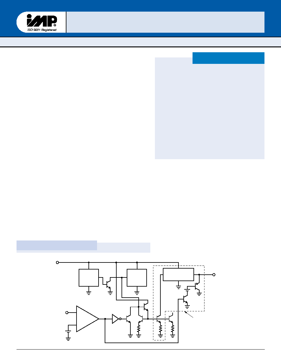
The IMP5115 SCSI terminator is part of IMP's family of high-perfor-
mance, adaptive, non-linear mode SCSI products, which are designed to
deliver true UltraSCSI performance in SCSI applications. The low voltage
BiCMOS architecture employed in its design offers performance superior
to older linear passive and active techniques. IMP's SCSI termination
architecture employs high-speed adaptive elements for each channel,
thereby providing the fastest response possible -- typically 35MHz,
which is 100 times faster than the older linear regulator/terminator
approach used by other manufacturers. Products using this older linear
regulator approach have bandwidths which are dominated by the output
capacitor and which are limited to 500KHz (see further discussion in the
Functional Description section). This new architecture also eliminates the
output compensation capacitor required in earlier terminator designs.
Each is approved for use with SCSI-1, -2, -3, UltraSCSI and beyond --
providing the highest performance alternative available today.
Another key improvement offered by the IMP5115 lies in its ability to
insure reliable, error-free communications even in systems which do not
adhere to recommended SCSI hardware design guidelines, such as the
use of improper cable lengths and impedances. Frequently, this situation
is not controlled by the peripheral or host designer and, when problems
occur, they are the first to be made aware of the problem. The IMP5115
architecture is much more tolerant of marginal system integrations.
Recognizing the needs of portable and configurable peripherals, the
IMP5115 has a TTL compatible sleep/disable mode. Quiescent current
is typically 375µA in this mode, while the output capacitance is also
less than 3pF. The obvious advantage of extended battery life for
portable systems is inherent in the product's sleep-mode feature.
Additionally, the disable function permits factory-floor or production-
line configurability, reducing inventory and product-line
diversity costs. Field configurability can also be accom-
plished without physically removing components which,
often times results in field returns due to mishandling.
Reduced component count is also inherent in the IMP5115
architecture. Traditional termination techniques require
large stabilization and transient protection capacitors of up
to 20µF in value and size. The IMP5115 architecture does
not require these components, allowing all the cost savings
associated with inventory, board space, assembly, reliability,
and component costs.
1
IMP5
IMP5
1
1
1
1
5
5
© 2000 IMP, Inc.
Data Communications 1
D
ATA
C
OMMUNICATIONS

2
408-432-9100/www.impweb.com
© 2000 IMP, Inc.
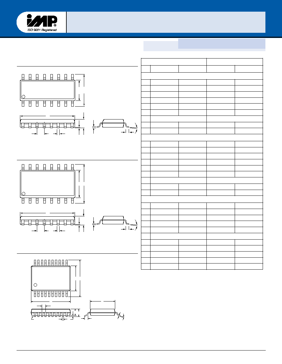
Pin Configuration
Ordering Information
Absolute Maximum Ratings
1
8
GND
1
TERM POWER
D Package
9
NC
7
NC
10 NC
6
D4
11 D5
5
D3
12 D6
4
D2
13 D7
3
D1
14 D8
2
D0
15 NC
16 DISABLE
5115__02.eps
IMP5115
8
GND
1
TERM POWER
DW Package
9
NC
7
NC
10 D5
6
D4
11 D6
5
D3
12 D7
4
D2
13 D8
3
D1
14 NC
2
D0
15 NC
16 DISABLE
5115__02a.eps
IMP5115
SO-16
SOWB-16
1
TERM POWER
PWP Package
7
D4
14 D6
8
HEAT SINK/GND
13 D5
9
NC
12 HEAT SINK/GND
10
GND
11 NC
6
D3
15 D7
5
D2
16 D8
4
D1
17 NC
3
D0
18 HEAT SINK/GND
2
HEAT SINK/GND
19 NC
20 DISABLE
5115_02b.eps
IMP5115
TSSOP-20
r
e
b
m
u
N
t
r
a
P
e
g
n
a
R
e
r
u
t
a
r
e
p
m
e
T
e
g
a
k
c
a
P
D
C
5
1
1
5
P
M
I
0∞
5
2
1
o
t
C
∞C
O
S
c
i
t
s
a
l
P
n
i
p
-
6
1
T
D
C
5
1
1
5
P
M
I
0∞
5
2
1
o
t
C
∞C
O
S
c
i
t
s
a
l
P
n
i
p
-
6
1
,
l
e
e
R
d
n
a
e
p
a
T
W
D
C
5
1
1
5
P
M
I
0∞
5
2
1
o
t
C
∞C
B
W
O
S
c
i
t
s
a
l
P
n
i
p
-
6
1
T
W
D
C
5
1
1
5
P
M
I
0∞
5
2
1
o
t
C
∞C
B
W
O
S
c
i
t
s
a
l
P
n
i
p
-
6
1
,
l
e
e
R
d
n
a
e
p
a
T
P
W
P
C
5
1
1
5
P
M
I
0∞
5
2
1
o
t
C
∞C
P
O
S
S
T
c
i
t
s
a
l
P
n
i
p
-
0
2
T
P
W
P
C
5
1
1
5
P
M
I
0∞
5
2
1
o
t
C
∞C
P
O
S
S
T
c
i
t
s
a
l
P
n
i
p
-
0
2
,
l
e
e
R
d
n
a
e
p
a
T
3
t
a
.
1
0
t
_
5
1
1
5
Thermal Data
Continuous Termination Voltage . . . . . . . . . . . 10V
Continuous Output Voltage Range . . . . . . . . 0V to 5.5V
Continuous Disable Voltage Range . . . . . . . . 0V to 5.5V
Operating Junction Temperature . . . . . . . . . . 0
∞
C to 125
∞
C
Storage Temperature Range . . . . . . . . . . . . . . ≠65
∞
C to 150
∞
C
Lead Temperature (Soldering, 10 sec.) . . . . . . 300
∞
C
Note:
1. Exceeding these ratings could cause damage to the device. All
voltages are with respect to Ground. Currents are positive
into, negative out of the specified terminal.
D Package:
Thermal Resistance Junction-to-Ambient,
JA
. . . . . . 120
∞
C/W
DW Package:
Thermal Resistance Junction-to-Ambient,
JA
. . . . . . 95
∞
C/W
PWP Package:
Thermal Resistance Junction-to-Ambient,
JA
. . . . . . 139
∞
C/W
Junction Temperature Calculation: T
J
= T
A
+ (P
D
x
JA
).
The
JA
numbers are guidelines for the thermal performance of the
device/pc-board system. All of the ambient airflow is assumed.
1
IMP5
IMP5
1
1
1
1
5
5

© 2000 IMP, Inc.
Data Communications 3
Recommended Operating Conditions
2
r
e
t
e
m
a
r
a
P
l
o
b
m
y
S
n
i
M
p
y
T
x
a
M
s
t
i
n
U
e
g
a
t
l
o
V
r
w
P
m
r
e
T
V
M
R
E
T
0
.
4
5
.
5
V
e
g
a
t
l
o
V
t
u
p
n
I
e
l
b
a
n
E
l
e
v
e
L
h
g
i
H
V
H
I
2
V
M
R
E
T
V
e
g
a
t
l
o
V
t
u
p
n
I
e
l
b
a
s
i
D
l
e
v
e
L
w
o
L
V
L
I
0
8
.
0
V
e
g
n
a
R
e
r
u
t
a
r
e
p
m
e
T
n
o
i
t
c
n
u
J
g
n
i
t
a
r
e
p
O
0
5
2
1
C
∞
.
l
a
n
o
i
t
c
n
u
f
s
i
e
c
i
v
e
d
e
h
t
h
c
i
h
w
r
e
v
o
e
g
n
a
r
e
h
t
e
t
a
c
i
d
n
i
s
n
o
i
t
i
d
n
o
c
g
n
i
t
a
r
e
p
o
d
e
d
n
e
m
m
o
c
e
R
.
2
:
e
t
o
N
s
p
e
.
2
0
t
_
5
1
1
5
Electrical Characteristics
Unless otherwise specified, these specifications apply at an ambient operating temperature of T
A
=
25
∞
C. TermPwr = 4.75V. Low duty cycle
pulse testing techniques are used which maintains junction and case temperatures equal to the ambient temperature.
r
e
t
e
m
a
r
a
P
l
o
b
m
y
S
s
n
o
i
t
i
d
n
o
C
n
i
M
p
y
T
x
a
M
s
t
i
n
U
e
g
a
t
l
o
V
h
g
i
H
t
u
p
t
u
O
V
T
U
O
5
6
.
2
5
8
.
2
V
t
n
e
r
r
u
C
y
l
p
p
u
S
r
w
P
m
r
e
T
I
C
C
n
e
p
O
=
s
e
n
il
a
t
a
d
ll
A
6
9
A
m
V
5
.
0
=
s
e
n
il
a
t
a
d
ll
A
5
1
2
5
2
2
V
8
.
0
<
n
i
P
e
l
b
a
s
i
D
5
7
3
µ
A
t
n
e
r
r
u
C
t
u
p
t
u
O
I
T
U
O
V
T
U
O
V
5
.
0
=
1
2
≠
3
2
≠
4
2
≠
A
m
t
n
e
r
r
u
C
t
u
p
n
I
e
l
b
a
s
i
D
I
N
I
V
5
7
.
4
=
n
i
P
e
l
b
a
s
i
D
0
1
A
n
V
0
=
n
i
P
e
l
b
a
s
i
D
0
9
≠
µ
A
t
n
e
r
r
u
C
e
g
a
k
a
e
L
t
u
p
t
u
O
I
L
O
V
,
V
8
.
0
<
n
i
P
e
l
b
a
s
i
D
O
V
5
.
0
=
0
1
A
n
e
d
o
M
e
l
b
a
s
i
D
n
i
e
c
n
a
t
i
c
a
p
a
C
C
T
U
O
V
T
U
O
z
H
M
1
=
y
c
n
e
u
q
e
r
F
,
V
0
=
3
F
p
h
t
d
i
w
d
n
a
B
l
e
n
n
a
h
C
W
B
5
3
z
H
M
l
e
n
n
a
h
C
r
e
p
,
t
n
e
r
r
u
C
k
n
i
S
n
o
i
t
a
n
i
m
r
e
T
I
K
N
I
S
V
T
U
O
V
4
=
0
6
A
m
s
p
e
.
3
0
t
_
5
1
1
5
1
IMP5
IMP5
1
1
1
1
5
5

4
408-432-9100/www.impweb.com
© 2000 IMP, Inc.
Application Information
IMP5115 Maximizes Line Current
Cable transmission theory suggests to optimize signal speed and
quality, the termination should act both as an ideal voltage refer-
ence when the line is released (deasserted) and as an ideal
current source when the line is active (asserted). Common active
terminators which consist of linear regulators in series with resis-
tors (typically 110
) are a compromise. With coventional linear
terminators as the line voltage increases the amount of current
decreases linearly by the equation;
The IMP5115, with its unique new architecture, applies the maxi-
mum amount of current regardless of line voltage until the
termination high threshold (2.85V) is reached.
Acting as a near ideal line terminator, the IMP5115 closely repro-
duces the optimum case when the device is enabled. To enable the
device the Disable pin must be driven LOW. When enabled,
quiescent current is 6mA and the device will respond to line
demands by delivering 24mA on assertion and by imposing 2.85V
on de-assertion.
Disable/Sleep Mode
Disable mode places the device in a sleep state, where quiescent
current typically 375
µ
A. When disabled, all outputs are in a high
impedance state. Sleep mode can be used for power conservation
or to remove the terminator from the SCSI chain.
An additional feature of the IMP5115 are their compatibility with
active negation drivers.
V
V
R
I
REF
LINE
-
(
)
=
.
Figure 3.
5115_03.eps
1 Meter, AWG 28
IMP5115
Receiver
Driver
IMP5115
Figure 1. Receiving Waveform ≠ 20MHz
Figure 2. Driving Waveform ≠ 20MHz
e
l
b
a
s
i
D
s
t
u
p
t
u
O
t
n
e
r
r
u
C
t
n
e
c
s
e
i
u
Q
H
d
e
l
b
a
n
E
A
m
6
L
e
c
n
a
d
e
p
m
I
h
g
i
H
/
d
e
l
b
a
s
i
D
5
7
3
µ
A
n
e
p
O
d
e
l
b
a
n
E
A
m
6
s
p
e
.
4
0
t
_
5
1
1
5
Table 1. Power Up/ Power Down Function Table
1
IMP5
IMP5
1
1
1
1
5
5
© 2000 IMP, Inc.
Data Communications
5
s
e
h
c
n
I
s
r
e
t
e
m
i
ll
i
M
n
i
M
x
a
M
n
i
M
x
a
M
*
)
n
i
P
-
6
1
(
O
S
A
3
5
0
.
0
9
6
0
.
0
5
3
.
1
5
7
.
1
1
A
4
0
0
.
0
0
1
0
.
0
0
1
.
0
5
2
.
0
B
4
1
0
.
0
8
1
0
.
0
5
3
.
0
6
4
.
0
C
7
0
0
.
0
0
1
0
.
0
9
1
.
0
5
2
.
0
D
5
8
3
.
0
4
9
3
.
0
8
7
.
9
1
0
.
0
1
E
0
5
1
.
0
8
5
1
.
0
1
8
.
3
1
0
.
4
e
C
S
B
0
5
0
.
0
C
S
B
7
2
.
1
H
8
2
2
.
0
4
4
2
.
0
9
7
.
5
0
2
.
6
L
0
2
0
.
0
0
3
0
.
0
1
5
.
0
7
7
.
0
)
n
i
P
-
6
1
(
B
W
O
S
A
3
9
0
.
0
4
0
1
.
0
5
3
.
2
5
6
.
2
1
A
4
0
0
.
0
2
1
0
.
0
0
1
.
0
0
3
.
0
B
0
1
0
.
0
8
1
0
.
0
5
2
.
0
6
4
.
0
C
9
0
0
.
0
3
1
0
.
0
3
2
.
0
2
3
.
0
D
--
0
2
4
.
0
--
7
6
.
0
1
E
5
9
2
.
0
5
0
3
.
0
9
4
.
7
5
7
.
7
e
C
S
B
0
5
0
.
0
C
S
B
7
2
.
1
H
4
0
4
.
0
9
1
4
.
0
6
2
.
0
1
5
6
.
0
1
L
5
2
0
.
0
5
3
0
.
0
4
6
.
0
9
8
.
0
)
n
i
P
-
0
2
(
P
O
S
S
T
A
8
6
0
.
0
8
7
0
.
0
3
7
.
1
9
9
.
1
B
9
0
0
.
0
5
1
0
.
0
5
2
.
0
8
.
0
C
5
0
0
.
0
8
0
0
.
0
3
1
.
0
2
2
.
0
D
3
0
3
.
0
1
1
3
.
0
0
7
.
7
0
9
.
7
E
5
0
2
.
0
2
1
2
.
0
0
2
.
5
8
3
.
5
F
C
S
B
5
2
0
.
0
C
S
B
7
2
.
1
G
2
0
0
.
0
8
0
0
.
0
5
0
.
0
1
2
.
0
H
4
6
0
.
0
2
7
0
.
0
3
6
.
1
3
8
.
1
L
5
2
0
.
0
7
3
0
.
0
5
6
.
0
5
9
.
0
M
∞
0
∞
8
∞
0
∞
8
P
1
0
3
.
0
1
1
3
.
0
5
6
.
7
0
9
.
7
C
A
2
1
0
-
S
M
g
n
i
w
a
r
D
C
E
D
E
J
*
3
t
a
.
5
0
t
_
5
1
1
5
H
E
e
B
D
A1
A
L
M
C
16-Pin (SO).eps
SO (16-Pin)
H
E
e
B
D
A1
A
L
M
C
16-Pin (SOWB).eps
SOWB (16-Pin)
3
2
1
E
P
D
SEATING PLANE B
G
A H
F
E
L
20-Pin (TSSOP).eps
C
M
TSSOP (20-Pin)
Package Dimensions
1
IMP5
IMP5
1
1
1
1
5
5