
ILC 6370/71
SOT-89 Step up Switching Regulator with Shutdown
Impala Linear Corporation
Impala Linear Corporation
1
(408) 574-3939
www.impalalinear.com
July 1999
ILC6370/1 1.3
50mA boost converter in 5-lead SOT-89 package. Only 3
external components are needed to complete the switcher
design, and frequency options of 50, 100, and 180kHz gives
the designer the ability to trade off system needs with
switcher design size.
87% max duty cycle gives conversion efficiencies of 85%.
Standard voltage options of 2.5V, 3.3V, and 5.0V at ±2.5%
accuracy feature on-chip phase compensation and soft-
start design.
ILC6371 drives an external transistor for higher current
switcher design, with all of the features and benefits of
the ILC6370.
!
85% efficiency at 50mA
!
Start-up voltages as low as 900mV
!
±2.5% accurate outputs
!
Complete switcher design with only 3 external components
!
50, 100 and 180kHz switching frequency versions available
!
Shutdown to 0.5µA
!
External transistor option allows several hundred milliamp
switcher design
!
Cellular Phones, Pagers
!
Portable Cameras and Video Recorders
!
Palmtops and PDAs
Ordering Information*
ILC6370CP-25
2.5V±2.5%@50kHz
ILC6370CP-25
3.3V±2.5%@50kHz
ILC6370CP-50
5.0V±2.5%@50kHz
ILC6370BP-25
2.5V±2.5%@100kHz
ILC6370BP-33
3.3V±2.5%@100kHz
ILC6370BP-50
5.0V±2.5%@100kHz
ILC6370AP-25
2.5V±2.5%@180kHz
ILC6370AP-33
3.3V±2.5%@180kHz
ILC6370AP-50
5.0V±2.5%@180kHz
ILC6371CP-25
2.5V±2.5%@50kHz, external xtor
ILC6371CP-33
3.3V±2.5%@50kHz, external xtor
ILC6371CP-50
5.0V±2.5%@50kHz, external xtor
ILC6371BP-25
2.5V±2.5%@100kHz, external xtor
ILC6371BP-33
3.3V±2.5%@100kHz, external xtor
ILC6371BP-50
5.0V±2.5%@100kHz, external xtor
ILC6371AP-25
2.5V±2.5%@180kHz, external xtor
ILC6371AP-33
3.3V±2.5%@180kHz, external xtor
ILC6371AP-50
5.0V±2.5%@180kHz, external xtor
Standard Product offering comes in tape and reel,
quantity 1000 per reel, orientation right for SOT-89
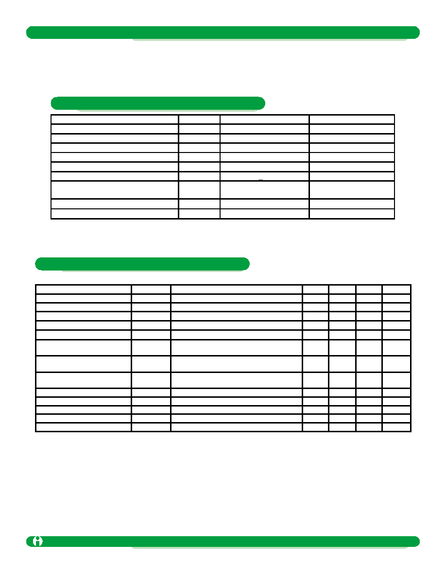
V
L X
LIMI TER
P WM Co ntrol led
BUFFER
L
X
V
SS
EXT
+
-
CHIP ENABLE
OSC
50/ 100/180KHz
V
DD
V
OUT
CE
P hase comp
V
re f
Slow Start
V
DD
is i nternall y connected to the V
O UT
pi n.
SOT -89-5
(TOP VI EW)
1
3
2
V
O UT
CE
L
X
4
5
V
SS
N/C
SOT -89-5
(TOP VI EW)
1
3
2
V
O UT
CE
EXT
4
5
V
S S
N/C
ILC6370
ILC6371
General Description
Features
Applications
Block Diagram
Pin-Package Configurations
SOT-89 Step up Switching Regulator with Shutdown
Impala Linear Corporation
2
(408) 574-3939
www.impalalinear.com
July 1999
ILC6370/1 1.3
Parameter
Symbol
Ratings
Units
V
OUT
Input Voltage Pin
V
OUT
12
V
CE Input Voltage
V
CE
12
V
Voltage on pin L
X
V
LX
12
V
Current on pin L
X
I
LX
400
mA
Voltage on pin EXT
V
EXT
0.3 ~V
OUT
+0.3
V
Current pin EXT
I
EXT
+50
mA
Continuous Total Power Dissipation
(SOT-89-5)
P
D
500
mW
Operating Ambient Temperature
T
OPR
-30~+80
C
Storage Temperature
T
STG
-40~+125
C
Parameter
Symbol
Conditions
Min
Typ
Max
Units
Output Voltage
V
OUT
3.218
3.300
3.383
V
Input Voltage
V
IN
10
V
Oscillation Startup Voltage
V
ST2
L
X
:10k
Pull-up to.5V, V
OUT
= V
ST
500
600
mA
Operation Startup Voltage
V
ST1
I
OUT
+1mA
55
86
µ
A
Supply Current 1
I
DD
1
L
X
:10k
Pull-up to.5V, V
OUT
= 4.5V
1.5
2.5
µ
A
Supply Current 1
I
DD
2
Open Loop Measurement, V
S/D
= V
IN
,
V
LX
=V
IN-
0.4V, V
OUT
= 3V
0.64
0.85
L
X
Switch-On Resistance
R
SWON
Open Loop Measurement, V
OUT
= V
IN,
V
LX
= 0V
2.0
µ
A
L
X
Leakage Current
I
L
X
L
Measure Waveform at EXT pin V
IN
= 3.6V
I
OUT
= 20mA
255
300
345
KHz
Oscillator Frequency
F
OSC
100
%
Maximum Duty Ratio
MAXDTY
No Load
10
17
25
%
Satndb-by Current
I
STB
95
%
CE "High " Voltage
V
CEH
Minimum V
IN
When V
ref
does not start up
1
1.8
V
CE "Low " Voltage
V
CEL
V
ref
rises to 0V from 0.9V
6.0
10.0
16.0
msec
Note: Unless otherwise spcified, V
IN
= V
OUT
x 0.6, I
OUT
= 50mA. See Schematic, figure 1.
Absolute Maximum Ratings (T
A
= 25∞C)
V
OUT
= 5.0V, F
OSC
= 100kHz, T
A
= 25∞C, Test Circuit of figure 1
Elcetrical Characteristics ILC6370BP-50
SOT-89 Step up Switching Regulator with Shutdown
Impala Linear Corporation
3
(408) 574-3939
www.impalalinear.com
July 1999
ILC6370/1 1.3
Parameter
Symbol
Conditions
Min Typ Max
Units
CE "High" Current
I
CEH
L
X
: 10k
pull-up to 5V, V
CE
= V
OUT
= 4.5V
0.25
µA
CE "Low" Current
I
CEL
L
X
: 10k
pull-up to 5V, V
OUT
=
4.5V, V
CE
= 0V
-0.25
µ
L
X
Limit Voltage
V
LXLMT
L
X
: 10k
pull-up to 5V, V
OUT
= 4.5V, F
OSC
> F
OSC
x 2
(1)
0.7
1.1
V
Efficiency
EFFI
85
%
Parameter
Symbol
Conditions
Min
Typ
Max
Units
Output Voltage
V
OUT
4.87
5
5.000 5.125 V
Input Voltage
V
IN
10
V
Oscillation Startup Voltage
V
ST
EXT: 10k
pull-up to 5V, V
OUT
= V
ST
0.8
V
Supply Current 1
I
DD
1
EXT: 10k
pull-up to 5V, V
OUT
= 4.5V
38.4
64.1
µA
Supply Current 2
I
DD
2
EXT: 10k
pull-up to 5V, V
OUT
= 5.5V
6.9
13.8
µA
EXT "High" On-Resistance R
EXTH
EXT: 10k
pull-up to 5V, V
OUT
= 4.5V,
V
EXT
= 4.1V
30
50
EXT "Low" On-Resistance
R
EXTL
V
EXT
= 0.4V, V
OUT
= 5.5V
30
50
Oscillator Frequency
F
OSC
EXT: 10k
pull-up to 5V, V
OUT
= 4.5V,
Measuring of EXT pin
85
100
115
kHz
Maximum Duty Ratio
MAXDTY EXT: 10k
pull-up to 5V, V
OUT
= 4.5V,
Measuring of EXT pin
80
87
92
%
Stand-by Current
I
STB
EXT: 10k
pull-up to 5V, V
OUT
= 4.5V
0.5
µA
CE "High" Voltage
V
CEH
EXT: 10k
pull-up to 5V, V
OUT
= 4.5V,
Existance of L
X
Oscillation
0.75
V
CE "Low" Voltage
V
CEL
EXT: 10k
pull-up to 5V, V
OUT
= 4.5V,
Stopped L
X
Oscillation
0.20
V
CE "High" Current
I
CEH
EXT: 10k
pull-up to 5V, V
OUT
= V
CE
= 4.5V
0.25
µA
CE "Low" Current
I
CEL
EXT: 10k
pull-up to 5V, V
OUT
= 4.5V, V
CE
= 0V
-0.25 µA
Efficiency
EFFI
85
%
Slow Start Time
T
SS
10
msec
V
OUT
= 5.0V, F
OSC
= 100kHz, T
A
= 25∞C; Test Circuit of figure 1
1. Switching frequency determined by delay time of internal comparator to turn L
X
"OFF," and minimum "ON" time as
determined by MAXDTY spec.
V
OUT
= 5.0V, F
OSC
= 100kHz, T
A
= 25∞C; Test Curcuit of figure 2.
Electrical Characteristics ILC6370BP-50
Electrical Characteristics ILC6371BP-50
SOT-89 Step up Switching Regulator with Shutdown
Impala Linear Corporation
4
(408) 574-3939
www.impalalinear.com
July 1999
ILC6370/1 1.3
Parameter
Slow Start Time
Symbol
T
SS
Conditons
Min
Typ
10
Max
Units
msec
V
OUT
= 5.0V, F
OSC
= 100kHz, T
A
= 25∞C; Test Circuit of figure 1
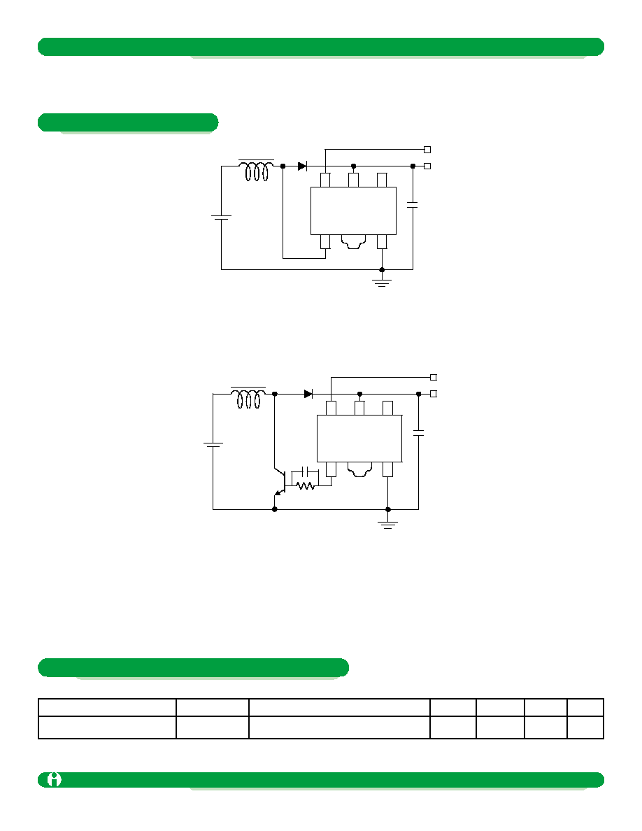
ILC6370
1
2
3
4
5
CE
V
OUT
C
L
+
GND
V
IN
L
SD
ILC6371
1
2
3
4
5
CE
V
OUT
C
L
+
L
SD
V
IN
GND
C
B
R
B
Tr
L: 100µH (SUMIDA, CD-54)
SD: Diode (Schottky diode; MATSUSHITA MA735)
C
L
: 16V 47µF (Tantalum Capacitor; NICHICON, F93)
L: 100µH (SUMIDA, CD-54)
SD: Diode (Schottky diode; MATSUSHITA MA735)
C
L
: 16V 47µF (Tantalum Capacitor; NICHICON, F93)
R
B
: 1k
C
B
: 3300pF
Tr: 2SC3279, 2SDI628G
Figure 1: Test Circuit
Figure 2: Test Circuit
Applications Circuits
Electrical Characteristics ILC6370BP-50

SOT-89 Step up Switching Regulator with Shutdown
Impala Linear Corporation
5
(408) 574-3939
www.impalalinear.com
July 1999
ILC6370/1 1.3
The ILC6370 performs boost DC-DC conversion by controlling the
switch element shown in the circuit below.
When the switch is closed, current is built up through the inductor.
When the switch opens, this current has to go somewhere and is
forced through the diode to the output. As this on and off switch-
ing continues, the output capacitor voltage builds up due to the
charge it is storing from the inductor current. In this way, the out-
put voltage gets boosted relative to the input. The ILC6370 mon-
itors the voltage on the output capacitor to determine how much
and how often to drive the switch.
In general, the switching characteristic is determined by the output
voltage desired and the current required by the load. Specifically
the energy transfer is determined by the power stored in the coil
during each switching cycle.
PL = (t
ON
, V
IN
)
The ILC6370 and ILC6371 use a PWM or Pulse Width Modulation
technique. The parts come in one of three fixed internal frequen-
cies: 50, 100, or 180kHz. The switches are constantly driven at
these frequencies. The control circuitry varies the power being
delivered to the load by varying the on-time, or duty cycle, of the
switch. Since more on-time translates to higher current build up in
the inductor, the maxmim duty cycle of the switch determines the
maximum load current that the device can support. The ILC6370
and ILC6371 both support up to 87% duty cycles, for maximum
usable range of load currents.
There are two key advantages of PWM type controllers. First,
because the controller automatically varies the duty cycle of the
switche's on-time in response to changing load conditions, the
PWM controller will always have an optimized waveform for a
steady-state load. This translates to very good efficiency at high
currents and minimal ripple on the output. [Ripple is due to the
output cap constanty accepting and storing the charge recieved
from the inductor, and delivering charge as required by the load.
The "pumping" action of the switch produces a sawtooth-shaped
voltage as seen by the output.]
The other key advatage of the PWM type controllers is that the
radiated noise due to the swtiching transients will always occur at
the (fixed) switching frequency. Many applications do not care
much about switching noise, but certain types of applications,
especially communication equipment, need to minimze the high
frequency interference within their system as much as is possible.
Using a boost converter requires a certain amount of higher fre-
quency noise to be generated; using a PWM converter makes that
noise highly predictable; thus easier to filter out.
There are downsides of PWM approaches, especially at very low
currents. Because the PWM technique relies on constant switch-
ing and varying duty cycle to match the load conditions, there is
some point where the load current gets to small to be handled effi-
ciently. If the ILC6370 had an ideal switch, this would not be such
a problem. But an actual switch consumes some finite amount of
current to switch on and off; at very low current this can be of the
same magnitude as the load current itself, driving switching effi-
ciencies down to 50% and below.
The other limitation of PWM techniques is that, while the funda-
mental switching frequency is easier to filter out since it's constant,
the higher order harmonics of PWM will be present and may have
to be filtered out as well. Any filtering rquirements will vary by appli-
cation and by actual system design and layout, so generalizations
in this area are difficult, at best. [For other boost converter tech-
niques, please see the ILC6380/81 and ILC6390/91 data sheets.]
However, PWM control for boost DC-DC conversion is widely
used, especially in audio-noise sensitive applications or applica-
tions requiring strict filtering of the high frequency components.
Impala's products give very good efficiencies of 85% at 50mA out-
put (5V operation), 87% maximum duty cycles for high load con-
ditions, while maintaining very low shutdown current levels of
0.5µA. The only difference between the ILC6370 and ILC6371
parts is that the 6371 is configured to drive an external transistor
as the switch element. Since larger transistors can be selected for
this element, higher effective loads can be regulated.
Start-up Mode
The ILC6370 has an internal soft-start mode which suppresses
ringing or overshoot on the output during start-up. The following
diagram illustrates this start-up condition's typical performance
External Components and Layout Consideration
The ILC6370 is designed to provide a complete DC-DC convertor
solution with a minmum of external components. Ideally, only
three externals are required: the inductor, a pass diode, and an
output capacitor.
The inductor needs to be of low DC Resistance type, typically 1
value. Toroidal wound inductors have better field containment (less
high frequency noise radiated out) but tend to be more expensive.
Some manufacturers like Coilcraft have new bobbin-wound induc-
tors with shielding included, which may be an ideal fit for these
applications. Contact the manufacturer for more information.
The inductor size needs to be in the range of 47µH to 1mH. In
general, larger inductor sizes deliver less current, so the load cur-
rent wil determine the inductor size used.
V
IN
- V
f
V
OUT MIN
T
SOFT-START
(~10msec)
t = 0
Functions and Operation