
100mA boost converter in 5-lead SOT-89 package using
both PFM and PWM conversion techniques. In normal
operation the ILC6380 runs in PWM mode running at one of
three fixed frequencies. At light loads the ILC6380 senses
when the duty cycle drops to approximately 10%, and auto-
matically switches into a power-saving PFM switching tech-
nique. This maintains high efficiencies both at full load and
in system sleep conditions.
Only 3 external components are needed to complete the
switcher design, and standard voltage options of 2.5, 3.3,
and 5.0V at ±2.5% accuracy feature on-chip phase com-
pensation and soft-start design.
ILC6381 drives an external transistor for higher current switch-
er design, with all of the features and benefits of the ILC6380.
ILC6380/81
SOT-89 Step-up Dual-Mode Switcher with Shutdown
Impala Linear Corporation
Impala Linear Corporation
1
(408) 574-3939
www.impalalinear.com
Sept 1999
ILC6380/1 1.4
!
85% efficiency at 50mA
!
Start-up voltages as low as 900mV
!
±2.5% accurate outputs
!
Complete switcher design with only 3 external
components
!
50, 100 and 180kHz switching frequency versions
available
!
Shutdown to 0.5µA I
q
!
External transistor option allows several hundred
milliamp switcher design
!
Cellular Phones, Pagers
!
Portable Cameras and Video Recorders
!
Palmtops and PDAs
SOT -89-5
(TOP VI EW)
1
3
2
V
O UT
CE
L
X
4
5
V
SS
N/C
SOT -89-5
(TOP VI EW)
1
3
2
V
O UT
CE
EXT
4
5
V
S S
N/C
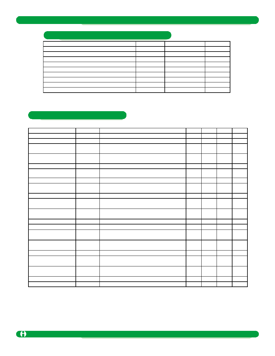
ILC6380CP-25
2.5V ± 2.5%@50kHz
ILC6380CP-33
3.3V ± 2.5%@50kHz
ILC6380CP-50
5.0V ± 2.5%@50khz
ILC6380CP-25
2.5V ± 2.5%@100kHz
ILC6380CP-33
3.3V ± 2.5%@100kHz
ILC6380CP-50
5.0V ± 2.5%@100kHz
ILC6380CP-25
2.5V ± 2.5%@180kHz
ILC6380CP-33
3.3V ± 2.5%@180kHz
ILC6380CP-50
5.0V ± 2.5%@180kHz
ILC6381CP-25
2.5V ± 2.5%@50kHz, external xtor
ILC6381CP-33
3.3V ± 2.5%@50kHz, external xtor
ILC6381CP-50
5.0V ± 2.5%@50kHz, external xtor
ILC6381BP-25
2.5V ± 2.5%@100kHz, external xtor
ILC6381BP-33
3.3V ± 2.5%@100kHz, external xtor
ILC6381BP-50
5.0V ± 2.5%@100kHz, external xtor
ILC6381AP-25
2.5V ± 2.5%@180kHz, external xtor
ILC6381AP-33
3.3V ± 2.5%@180kHz, external xtor
ILC6381AP-50
5.0V ± 2.5%@180kHz, external xtor
V
L X
LIMI TER
PWM/ PFM Controll ed
BUFFER
L
X
V
SS
EXT
+
-
CHI P ENABLE
OSC
50/ 100/180KHz
V
DD
V
OUT
CE
Phase comp
V
r ef
Slow Start
V
DD
is i nternall y connected to the V
O UT
pi n.
*
Standard product offering comes in tape & reel, quantity
1000 per reel, orientation right for SOT-89
General Description
Package Features
Applications
Block Diagram
Pin Package Configurations
Ordering Information
SOT-89 Step-up Dual-Mode Switcher with Shutdown
Impala Linear Corporation
2
(408) 574-3939
www.impalalinear.com
Sept 1999
ILC6380/1 1.4
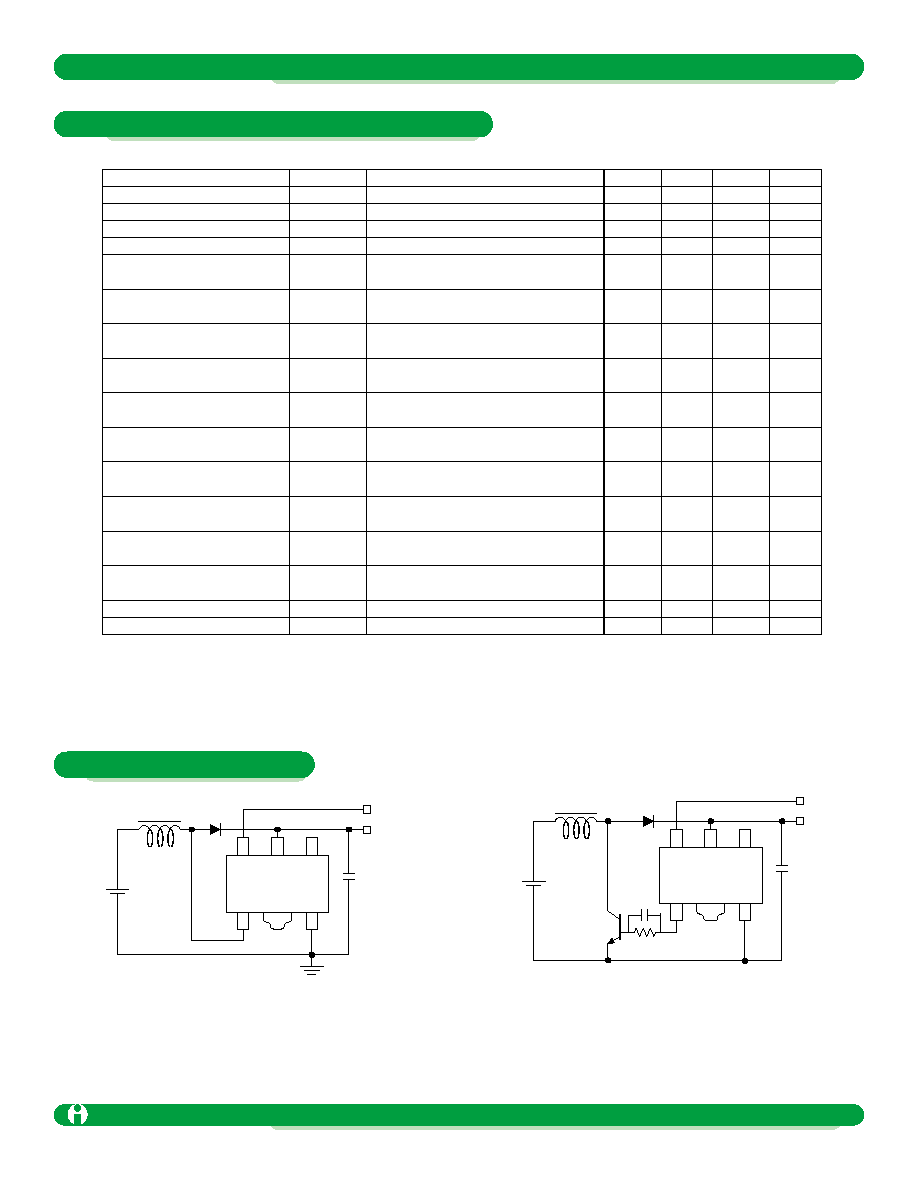
Parameter
Symbol
Ratings
Units
V
OUT
Input Voltage
V
OUT
12
V
Voltage on pin L
X
V
LX
12
V
Current on pin L
X
I
LX
400
mA
Voltage on pin EXT
V
EXT
V
SS
-0.3~V
OUT
+0.3
V
Current on pin EXT
I
EXT
±50
mA
CE Input Voltage
V
CE
12
V
Continuous Total Power Dissipation
P
D
500
mW
Operating Ambient Temperature
T
OPR
-30~+80
∞C
Storage Temperature
T
STG
-40~+125
∞C
Stresses above those listed under ABSOLUTE MAXIMUM RATINGS may cause permanent device failure. Functionality at
or above these limits is not implied. Exposure to absolute maximum ratings for extended periods may affect device reliabil-
ity. Operating ranges define those limits between which the functionality of the device is guaranteed.
Notes:
1. The Schottky diode (S.D.), in figure 3 must be type MA735, with Reverse current (IR) < 1.0µA at reverse voltage (VR)=10.0V
2. "Supply Current 1" is the supply current while the oscillator is continuously oscillating. In actual operation the oscillator
periodically operates which results in less average power consumption.
The current that is actually provided by external VIN source is represented by "No-Load Input Current(IIN)"
3. Switching frequency is determined by delay time of internal comparator to turn Lx "off", and minimum "on" time as determined
by MAXDTY spec.
Parameter
Symbol
Conditions
Min
Typ
Max
Units
Output Voltage
V
OUT
4.875 5.000 5.125
V
Input Voltage
V
IN
10
V
Oscillation Startup
Voltage
V
ST
L
X
= 10k
pull-up to 5V, V
OUT
= V
ST
0.8
V
Operation Startup
Voltage
V
ST1
I
OUT
= 1mA
0.9
V
No-Load Input Current
I
IN
I
OUT
= 0mA
(See Note 1)
23.0
46.0
µA
Supply Current 1
(See Note 2)
I
DD
1
L
X
= 10k
pull-up to 5V, V
OUT
= 4.5V
78.6
131.1
µA
Supply Current 2
I
DD
2
L
X
= 10k
pull-up to 5V, V
OUT
= 5.5V
6.9
13.8
µA
L
X
Switch-On
Resistance
R
SWON
L
X
= 10k
pull-up to 5V, V
OUT
= 4.5V
1.3
2.3
L
X
Leakage Current
I
LXL
No external components, V
OUT
= VL
X
= 10V
1.0
µA
Oscillator Freq.
F
OSC
L
X
= 10k
pull-up to 5V, V
OUT
= 4.5V,
Measuring of L
X
waveform
85
100
115
kHz
Maximum Duty Ration
MAXDTY L
X
= 10k
pull-up to 5V, V
OUT
= 4.5V,
Measuring of L
X
on-time
80
87
92
%
PFM Duty Ration
PFMDTY V
IN
= 4.75V, Measuring of L
X
on-time
5
10
20
%
Stand-by Current
I
STB
L
X
= 10k
pull-up to 5V, V
OUT
=4.5V
0.5
µA
CE "High" Voltage
V
CEH
L
X
= 10k
pull-up to 5V, V
OUT
= 4.5V,
Existence of L
X
Oscillation
0.75
V
CE "Low" Voltage
V
CEL
L
X
= 10k
pull-up to 5V, V
OUT
= 4.5V,
Stopped L
X
Oscillation
0.20
V
CE "High" Current
I
CEH
L
X
= 10k
pull-up to 5V, V
OUT
= V
CE
= 4.5V
0.25
µA
CE "Low" Current
I
CEL
L
X
= 10k
pull-up to 5V, V
OUT
= 4.5V,
V
CE
= 0V
-0.25
µA
L
X
Limit Voltage
V
LXLMT
L
X
= 10k
pull-up to 5V, V
OUT
= 4.5V,
F
OSC
> F
OSC
x 2
(See Note 2)
0.7
1.1
V
Efficiency
EFFI
85
%
Slow Start Time
T
SS
10
msec
V
OUT
= 5.0V, F
OSC
= 100kHz T
A
- 25∞C. Unless otherwise specified, V
IN
= V
OUT
x 0.6, I
OUT
= 50mA. See schematic, figure 3
Absolute Maximum Ratings (T
A
= 25∞C)
Electrical Characteristics
SOT-89 Step-up Dual-Mode Switcher with Shutdown
Impala Linear Corporation
3
(408) 574-3939
www.impalalinear.com
Sept 1999
ILC6380/1 1.4
V
OUT
= 5.0V, F
OSC
= 100kHz T
A
= 25∞C. Unless otherwise specified, V
IN
= V
OUT
X0.6, I
OUT
= 50mA. See the schematic, figure 4.
ILC6380
1
2
3
4
5
CE
V
OUT
C
L
+
GND
V
IN
L
SD
ILC6381
1
2
3
4
5
CE
V
OUT
C
L
+
L
SD
V
IN
C
B
R
B
Tr
L: 100µH ( SUMIDA, CD-54)
SD: Diode (Schottky diode; MATSUSHITA MA735)
CL: 16V 47µF (Tantalum Capacitor; NICHICON, F93)
L: 47µH ( SUMIDA, CD-54)
SD: Diode (Schottky diode; MATSUSHITA MA735)
CL: 16V 47µF (Tantalum Capacitor; NICHICON, F93)
RB: 1kW
CB: 3300pF
Tr: 2SC3279, 2SDI628G
Parameter
Symbol
Conditions
Min
Typ
Max
Units
Output Voltage
V
OUT
Test Circuit of Figure 2
4.875 5.000 5.125
V
Input Voltage
V
IN
10
V
Oscillation Startup Voltage
V
ST2
V
OUT
= V
ST2
0.8
V
Operation Startup Voltage
V
ST1
I
OUT
= 1mA
0.9
V
Supply Current 1
(See Note 2)
I
DD
1
EXT = 10k
pull-up to 5V,
V
OUT
= 4.5V
78.6
131.1
µA
Supply Current 2
I
DD
2
EXT = 10k
pull-up to 5V,
V
OUT
= 5.5V
6.9
13.8
µA
EXT "High" On-Resistance
R
EXTH
EXT = 10k
pull-up to 5V,
V
OUT
= 4.5V, V
EXT
=
V
OUT
≠ 0.4V
30
50
EXT "Low" On-Resistance
R
EXTL
EXT = 10
pull-up to 5V,
V
OUT
= 4.5V, V
EXT
= V
OUT
- 0.4V
30
50
Oscillator Frequency
F
OSC
EXT = 10k
pull-up to 5V, V
OUT
=
4.5V, Measuring of EXT waveform
85
100
115
kHz
Maximum Duty Ratio
MAXDTY EXT = 10k
pull-up to 5V, V
OUT
=
4.5V, Measuring of EXT high state
80
87
92
%
CE "High" Voltage
V
CEH
EXT = 10k
pull-up to 5V, V
OUT
=
4.5V, Existence of Oscillation
0.75
V
CE "Low" Voltage
V
CEL
EXT = 10k
pull-up to 5V, V
OUT
=
4.5V, Stopped EXT Oscillation
0.20
V
CE "High" Current
I
CEH
EXT: 10k
pull-up to 5V,
V
OUT
= 4.5V, V
CE
= V
OUT
X 0.95V
0.25
µA
CE "Low" Current
I
CEL
EXT = 10k
pull-up to 5V,
V
OUT
= 4.5V, V
CE
= 0V
-0.25
µA
Efficiency
EFFI
85
%
Slow Start Time
T
SS
10
msec
Notes:
1. The Schottky diode (S.D.), in figure 3 must be type MA735, with Reverse current (IR) < 1.0µA at reverse voltage (VR)=10.0V
2. "Supply Current 1" is the supply current while the oscillator is continuously oscillating. In actual operation the oscillator periodically
operates which results in less average power consumption.
The current that is actually provided by external V
IN
source is represented by "No-Load Input Current (I
IN
)"
Electrical Characteristics ILC6380BP-50
Typical Applications
Figure 3
Figure 4

SOT-89 Step-up Dual-Mode Switcher with Shutdown
Impala Linear Corporation
4
(408) 574-3939
www.impalalinear.com
Sept 1999
ILC6380/1 1.4
The ILC6380 performs boost DC-DC conversion by controlling the
switch element shown in the circuit below
When the switch is closed, current is built up through the inductor.
When the switch opens, this current has to go somewhere and is
forced through the diode to the output. As this on and off switch-
ing continues, the output capacitor voltage builds up due to the
charge it is storing from the inductor current. In this way, the out-
put voltage gets boosted relative to the input. The ILC6380 moni-
tors the voltage on the output capacitor to determine how much
and how often to drive the switch.
In general, the switching characteristic is determined by the output
voltage desired and the current required by the load. Specifically
the energy transfer is determined by the power stored in the coil
during each switching cycle.
PL = (t
ON
, V
IN
)
The ILC6380 and ILC6381 use a PWM or Pulse Width Modulation
technique. The parts come in one of three fixed internal frequen-
cies: 50, 100, or 180kHz. The switches are constantly driven at
these frequencies. The control circuitry varies the power being
delivered to the load by varying the on-time, or duty cycle, of the
switch. Since more on-time translates to higher current build-up in
the inductor, the maximum duty cycle of the switch determines the
maximum load current that the device can support. The ILC6380
and ILC6381 both support up to 87% duty cycles, for maximum
usable range of load currents.
There are two key advantages of the PWM type controllers. First,
because the controller automatically varies the duty cycle of the
switch's on-time in response to changing load conditions, the
PWM controller will always have an optimized waveform for a
steady-state load. This translates to very good efficiency at high
currents and minimal ripple on the output. [Ripple is due to the out-
put cap constantly accepting and storing the charge received from
the inductor, and delivering charge as required by the load. The
"pumping" action of the switch produces a sawtooth-shaped volt-
age as seen by the output.]
The other key advantage of the PWM type controllers is that the
radiated noise due to the switching transients will always occur at
the (fixed) switching frequency. Many applications do not care
much about switching noise, but certain types of applications,
especially communication equipment, need to minimize the high
frequency interference within their system as much as is possible.
Using a boost converter requires a certain amount of higher fre-
quency noise to be generated; using a PWM converter makes that
noise highly predictable; thus easier to filter out.
Dual Mode Operation
But there are downsides of PWM approaches, especially at very
low currents. Because the PWM technique relies on constant
switching and varying duty cycle to match the load conditions,
there is some point where the load current gets too small to be
handled efficiently. An actual switch consumes some finite amount
of current to switch on and off; at very low currents this can be of
the same magnitude as the load current itself, driving switching
efficiencies down to 50% and below. The ILC6380 and ILC6381
overcome this limitation by automatically switching over to a PFM,
or Pulse Frequency Modulation, technique at low currents. This
technique conserves power loss by only switching the output if the
current drain requires it. As shown in the diagram below, the wave-
form actually skips pulses depending on the power needed by the
output. [This technique is also called "pulse skipping" because of
this characteristic.]
In the ILC6380 and ILC6381, this switchover is internally set to be
at the point where the PWM waveform hits approximately 10%
duty cycle. So the PFM mode is running at 10% duty cycle at the
rated frequency; for 100kHz part this means a constant on-time of
1msec. This not only is ideal for efficiency at these low currents,
but a 10% duty cycle will have much better output ripple charac-
teristics than a similarly configured PFM part, such as the ILC6390
and ILC6391.
The Dual-Mode architecture was designed specifically for those
applications, like communications, which need the spectral pre-
dictability of a PWM-type DC-DC converter, yet which also needs
the highest efficiencies possible, especially in Shutdown or
Standby mode. [For other conversion techniques, please see the
ILC6370/71 and ILC6390/91 datasheets.]
Other Considerations
The other limitation of PWM techniques is that, while the funda-
mental switching frequency is easier to filter out since it's constant,
the higher order harmonics of PWM will be present and may have
to be filtered out, as well. Any filtering requirements, though, will
vary by application and by actual system design and layout, so
generalizations in this area are difficult, at best.
However, PWM control for boost DC-DC conversion is widely
used, especially in audio-noise sensitive applications or applica-
tions requiring strict filtering of the high frequency components.
Impala's products give very good efficiencies of 85% at 50mA out-
put (5V product), 87% maximum duty cycles for high load condi-
tions, while maintaining very low shutdown current levels of
V
SET
V
OUT
Switch Waveform
Functions and Operation
SOT-89 Step-up Dual-Mode Switcher with Shutdown
Impala Linear Corporation
5
(408) 574-3939
www.impalalinear.com
Sept 1999
ILC6380/1 1.4
0.5mA. The only difference between the ILC6380 and ILC6381
parts is that the 6381 is configured to drive an external transistor
as the switch element. Since larger transistors can be selected for
this element, higher effective loads can be regulated.
Start-up Mode
The ILC6380 has an internal soft-start mode which suppresses
ringing or overshoot on the output during start-up. The following
diagram illustrates this start-up condition's typical performance:
External Components and Layout Consideration
The ILC6380 is designed to provide a complete DC-DC convertor
solution with a minimum of external components. Ideally, only
three externals are required: the inductor, a pass diode, and an
output capacitor.
The inductor needs to be of low DC Resistance type, typically 1
value. Toroidal wound inductors have better field containment (less
high frequency noise radiated out) but tend to be more expensive.
Some manufacturers like Coilcraft have new bobbin-wound induc-
tors with shielding included, which may be an ideal fit for these
applications. Contact the manufacturer for more information.
The inductor size needs to be in the range of 47mH to 1mH. In
general, larger inductor sizes deliver less current, so the load cur-
rent will determine the inductor size used.
For load currents higher than 10mA, use an inductor from 47mH
to 100mH. [The 100mH inductor shown in the datasheet is the
most typical used for this application.]
For load currents of around 5mA, such as pagers, use an inductor
in the range of 100mH to 330mH. 220mH is the most typical value
used here.
For lighter loads, an inductor of up to 1mH can be used. The use
of a larger inductor will increase overall conversion efficiency, due
to the reduction in switching currents through the device.
For the ILC6381, using an external transistor, the use of a 47mH
inductor is recommended based on our experience with the part.
Note that these values are recommended for both 50kHz and
100kHz operation. If using the ILC6380 or ILC6381 at 180kHz,
the inductor size can be reduced to approximately half of these
stated values.
The capacitor should, in general, always be tantalum type, as tan-
talum has much better ESR and temperature stability than other
capacitor types. NEVER use electrolytics or chemical caps, as the
C-value changes below 0◊C so much as to make the overall
design unstable.
Different C-values will directly impact the ripple seen on the output
at a given load current, due to the direct charge-to-voltage rela-
tionship of this element. Different C-values will also indirectly affect
system reliability, as the lifetime of the capacitor can be degraded
by constant high current influx and outflux. Running a capacitor
near its maximum rated voltage can deteriorate lifetime as well;
this is especially true for tantalum caps which are particularly sen-
sitive to overvoltage conditions.
In general, then, this capacitor should always be 47mF, Tantalum,
16V rating.
The diode must be of shottkey type for fast recovery and minimal
loss. A diode rated at greater than 200mA and maximum voltage
greater than 30V is recommended for the fastest switching time
and best reliability over time. Different diodes may introduce dif-
ferent levels of high frequency switching noise into the output
waveform, so trying out several sources may make the most
sense for your system.
For the IL6381, much of the component selection is as described
above, with the addition of the external NPN transistor and the
base drive network. The transistor needs to be of NPN type, and
should be rated for currents of 2A or more. [This translates to
lower effective on resistance and, therefore, higher overall effi-
ciencies.] The base components should remain at 1k
and
3300pF; any changes need to be verified prior to implementation.
As for actual physical component layout, in general, the more
compact the layout is, the better the overall performance will be. It
is important to remember that everything in the circuit depends on
a common and solid ground reference. Ground bounce can direct-
ly affect the output regulation and presents difficult behavior to
predict. Keeping all ground traces wide will eliminate ground
bounce problems.
It is also critical that the ground pin of C
L
and the V
SS
pin of the
device be the same point on the board, as this capacitor serves
two functions: that of the output load capacitor, and that of the
input supply bypass capacitor.
Layouts for DC-DC converter designs are critical for overall per-
formance, but following these simple guidelines can simplify the
task by avoiding some of the more common mistakes made in
these cases. Once actual performance is completed, though, be
sure to double-check the design on actual manufacturing proto-
type product to verify that nothing has changed which can affect
the performance.
V
IN
- V
f
V
OUT MIN
T
SOFT-START
(~10msec)
t = 0
SOT-89 Step-up Dual-Mode Switcher with Shutdown
Impala Linear Corporation
6
(408) 574-3939
www.impalalinear.com
Sept 1999
ILC6380/1 1.4
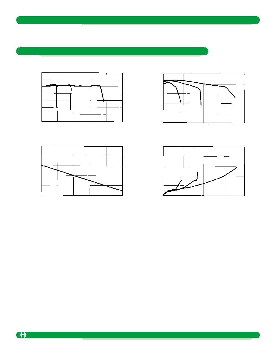
RIPPLE VOLTAGE vs. OUTPUT CURRENT
OUTPUT VOLTAGE vs. OUTPUT CURRENT
ILC6380CP-30
ILC6380CP-30
ILC6380CP-30
ILC6380CP-30
3.2
3.1
3.0
2.9
2.8
2.7
2.6
0
0 40 80 120 160 200
OUTPUT CURRENT I
OUT
(mA)
INPUT VOLTAGE V
IN
(V)
OUTPUT CURRENT I
OUT
(mA)
OUTPUT CURRENT I
OUT
(mA)
OUTPUT VOL
T
AGE V
OUT
(V)
EFFICIENCY
: EFFI (%)
RIPPLE V
r
(mV
p-p
)
INPUT CURRENT (µA)
L = 1000µH
C = 47µF (Tantalum)
L = 1000µH
C = 47µF (Tantalum)
L = 1000µH
C = 47µF (Tantalum)
V
IN
= 1.0V
V
IN
= 1.0V
V
IN
= 1.0V
V
IN
= 1.5V
V
IN
= 1.5V
V
IN
= 1.5V
V
IN
= 2.0V
V
IN
= 2.0V
V
IN
= 2.0V
100
80
60
40
20
0
0 40 80 120 160
EFFICIENCY vs. OUTPUT CURRENT
L = 100µH
R
L
= 0
C = 47µF (Tantalum)
I
OUT
= 0 (no load)
1.0 1.2 1.4 1.6 1.8 2.0
50
40
30
20
10
0
INPUT CURRENT vs. INPUT VOLTAGE
100
80
60
40
20
0
0 40 80 120 160
Typical Performance Characteristics
General conditions for all curves