
The ILC6382 series of step-up DC-DC converters operate
from 1-cell to 3-cell input. In shutdown mode, the device
allows true load disconnect from battery input. Designed for
wireless communications applications, the oscillator fre-
quency is set at 300kHz with no harmonics at sub 20kHz
audio band or at 455kHz IF band. Oscillator frequency is
externally synchronizable from 200kHz to 400kHz.
Internal synchronous rectification and dual PFM/PWM
mode of operation allows greater than 90% efficiency at
light and full load. The ILC6382 is capable of delivering
75mA at 3.3V output from a single cell input.The ILC6382-
XX offers 3.3V or 5V fixed output voltage while the
ILC6382-Adj allows adjustable output voltage to 6V maxi-
mum. Output voltage accuracy is +2% over specified tem-
perature range.
Additional features include power good output (POK) and an
internal low battery detector with 100s transient rejection
delay. The device will reject low battery input transients
under 100msec in duration. The ILC6382 series is available
in a space saving eight lead micro SOP (MSOP-8) package.
ILC6382
1-Cell to 3-Cell Boost with True Load Disconnect,
3.3V, 5V or Adjustable Output
Impala Linear Corporation
Impala Linear Corporation
1
(408) 574-3939
www.impalalinear.com
Oct 1999
ILC6382 1.5
!
0.9V to 6V input voltage
!
Guaranteed start up at 0.9V input
!
Synchronous rectification requires no external diode
!
True load disconnect from battery input in shutdown
!
Up to 75mA@3.3V and 40mA@5V from 1V input
!
Up to 375mA@3.3V and 160mA@5V from 3V input
!
Efficiency > 90% from 10mA to 150mA at V
OUT
= 5V
!
1
�
A battery input current in shutdown (with V
OUT
= 0V)
!
Internal Oscillator frequency : 300kHz to �15%
!
External freq synchronization from 150kHz to 500kHz
!
ILC6382 : Fixed 3.3V or 5V output
!
ILC6382-Adj : Adjustable output to 6V maximum
!
Low battery detector with 100ms transient rejection delay
!
Powergood output flag when V
OUT
is in regulation
!
Cellular Phones, Pagers
!
Palmtops, PDAs and portable electronics
!
High efficiency 1V step up converters
10�
F
ON
OFF
V
IN
1 to 3-cell
R5
R6
15
�
H
L
C
OUT
R1
R2
ILC6382-ADJ
MSOP-8
L
X
V
IN
LBI/SD
SYNC
GND
LBO
V
FB
V
OUT
V
OUT
V
OUT
= 1.25 (1+R1/R2)
1
2
3
4
8
7
6
5
C
IN
+
+
10
�
F
ILC6382-XX
1
3
2
4
8
6
7
5
L
X
V
IN
LBI/SD
SYNC
GND
LBO
POK
V
OUT
ON
OFF
V
IN
1 to 3-cell
R5
R6
15
�
H
MSOP-8
L
V
OUT
10�F
C
OUT
Low Battery
Detector Output
Power Good Output
C
IN
+
+
10�
F
Ext
Sync
Ext
Sync
(Note: Pin 9 should be connected to ground if unused.)
General Description
Features
Applications
Typical Circuit
Figure 1: ILC6382
Figure 2: ILC6382-Adj

1-Cell to 3-Cell Boost with True Load Disconnect, 3.3V, 5V, or Adjustable Output
Impala Linear Corporation
2
(408) 574-3939
www.impalalinear.com
Oct 1999
ILC6382 1.5
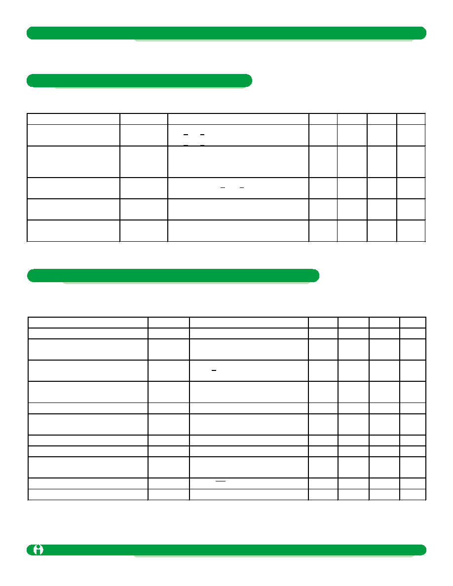
Pin Number
Pin Name
Pin Description
1
L
x
Inductor input. Inductor L connected between this pin and the battery
2
V
IN
Connect directly to battery
3
LBI/SD
Low battery detect input and shutdown. Low battery detect threshold is set with this pin
using a potential divider. If this pin is pulled to logic low then the device will shutdown.
4
SYNC
A logic level signal referenced to V
IN
, at a frequency between 150kHz and 500kHz on
this pin will override the internal 300kHz oscillator. If the SYNC function is unused then
pin 4 should be connected to ground
5
POK
(ILC6382CIR-XX)
This open drain output pin will go high when output voltage is within regulation,
0.92*V
OUT
(NOM)
< V
OUT
< 0.98*V
OUT
(NOM)
V
FB
(ILC6382CIR-ADJ)
This pin sets the adjustable output voltage via an external resistor divider network. The
formula for choosing the resistors is shown in the "Applications Information" section.
6
LBO
This open drain output will go low if the battery voltage is below the low battery
threshold set at pin 3
7
GND
Connect this pin to the battery and system ground
8
V
OUT
This is the regulated output voltage
Ordering Information* (T
A
= -40�C to + 85�C)
ILC6382CIR-33
3.3V output, MSOP-8 package
ILC6382CIR-50
5V output, MSOP-8 package
ILC6382CIR-ADJ
Adjustable output, MSOP-8 package
MSOP
(TOP VIEW)
ILC6382CIR-XX
SYNC
LB/SD
V
IN
L
X
1
2
3
4
5
6
7
8
V
OUT
GND
LBO
POK
SYNC
LB/SD
V
IN
L
X
1
2
3
4
5
6
7
8
V
OUT
GND
LBO
V
FB
MSOP
(TOP VIEW)
ILC6382CIR-ADJ
Pin-Package Configurations
Pin Functions ILC6382

1-Cell to 3-Cell Boost with True Load Disconnect, 3.3V, 5V, or Adjustable Output
Impala Linear Corporation
3
(408) 574-3939
www.impalalinear.com
Oct 1999
ILC6382 1.5
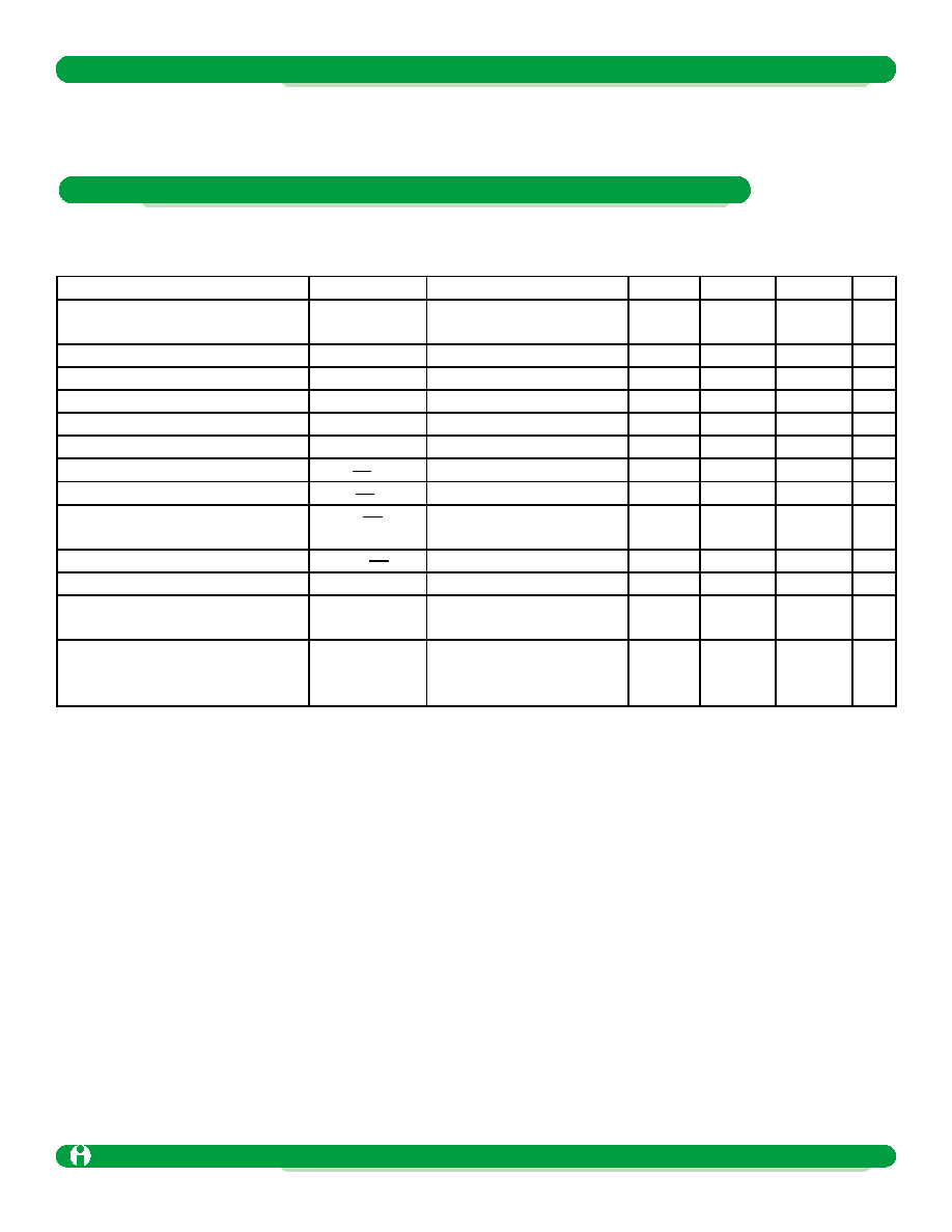
Parameter
Symbol
Conditions
Min
Typ
Max
Units
Output Voltage
V
OUT
0.9V < V
IN
< 3V, I
OUT
= 0mA
0.9V < V
IN
< 3V, I
OUT
= 0mA
3.234
3.201
3.300
3.366
3.399
V
Output Current
I
OUT
V
IN
= 0.9V, V
OUT
= V
OUT(nom)
� 4%
V
IN
= 1.2V, V
OUT
= V
OUT(nom)
� 4%
V
IN
= 2.4V, V
OUT
= V
OUT(nom)
� 4%
V
IN
= 3.0V, V
OUT
= V
OUT(nom)
� 4%
50
75
200
375
mA
Load Regulation
V
OUT
V
OUT (no load)
V
IN
= 1.2V, 0mA < I
OUT
< 50mA
V
IN
= 1.2V, 0mA < I
OUT
< 75mA
1.5
2.4
%
No Load Battery Input Current
I
IN( no load )
V
IN
= 1.2V, I
OUT
= 0mA
250
�A
Efficiency
V
IN
= 1.2V, I
OUT
= 3mA
V
IN
= 1.2V, I
OUT
=30mA
82
90
%
Parameter
Symbol
Ratings
Units
Voltage on V
OUT
pin
V
OUT
-0.3 to 7
V
Voltage on LBI, Sync, LBO, POK, V
FB
, L
X
and V
IN
pins
-
-0.3 to 7
V
Peak switch current on L
X
pin
IL
X
1
A
Current on LBO pin
I
sink(LBO)
5
mA
Continuous total power dissipation at 85 �C
P
d
400
mW
Short circuit current
I
SC
Internally protected
(1 sec duration)
A
Operating ambient temperature
T
A
-40 to 85
�C
Maximum junction temperature
T
J (max)
170
�C
Storage temperature
T
stg
-40 to 125
�C
Lead temperature (soldering 10 sec)
300
�C
Package thermal resistance
JA
206
�C/W
Unless otherwise specified all limits are at V
OUT
=3.3V, V
IRI
= 1.5V, Fosc = 300kHz and T
A
= 25�C. Test circuit of figure 1.
BOLDFACE type indicates limits that apply over the full operating temperature range. Note 2.
Absolute Maximum Ratings (Note 1)
Electrical Characteristics ILC6382CIR-33
1-Cell to 3-Cell Boost with True Load Disconnect, 3.3V, 5V, or Adjustable Output
Impala Linear Corporation
4
(408) 574-3939
www.impalalinear.com
Oct 1999
ILC6382 1.5
Unless otherwise specified all limits are at V
OUT
= 5V, V
IRI
= 1.5V, Fosc = 300kHz and T
A
= 25�C. Test circuit of figure 1.
BOLDFACE type indicates limits that apply over the full operating temperature range. Note 2.
Parameter
Symbol
Conditions
Min
Typ
Max
Units
Output Voltage
V
OUT
0.9V < V
IN
< 3V, I
OUT
= 0mA
0.9V < V
IN
< 3V, I
OUT
= 0mA
4.950
4.900
5.000
5.050
5.100
V
Output Current
I
OUT
V
IN
= 1.2V, V
OUT
= V
OUT(nom)
� 4%
V
IN
= 2.4V, V
OUT
= V
OUT(nom)
� 4%
V
IN
= 3.0V, V
OUT
= V
OUT(nom)
� 4%
50
110
160
mA
Load Regulation
V
IN
= 2.4V, 0mA < I
OUT
< 60mA
3
%
No Load Battery
Input Current
I
IN ( no load )
V
IN
= 2.4V, I
OUT
= 0mA
250
�A
Efficiency
V
IN
= 2.4V, I
OUT
= 3mA
V
IN
= 2.4V, I
OUT
=100mA
85
92
%
Unless otherwise specified all limits are at V
IN
= 2.4V, V
IRI
= 1.5V, Fosc = 300kHz, I
OUT
= 0mA and T
A
= 25�C. Test cir-
cuits of figure 1 and figure 2 for ILC6382CIR-XX and ILC6382CIR-ADJ respectively. BOLDFACE type indicates limits
that apply over the full operating temperature range. Note 2.
Parameter
Symbol
Conditions
Min
Typ
Max
Units
Minimum startup voltage
V
IN(start)
I
OUT
= 0mA
0.9
1
V
Input voltage range
V
IN
V
OUT =
V
OUT(nominal) � 4%
I
OUT
= 0mA (Note 3)
0.9
1
6
6
V
Battery input current in load
disconnect mode
I
IN(SD)
V
LBI/SD
< 0.4V, V
OUT
= 0V
(short circuit)
1
2
A
Switch on resistance
R
ds(on)
N-Channel MOSFET
P-Channel MOSFET
400
750
m
Oscillator frequency
f
osc
255
300
345
kHz
External clock frequency range
(sync)
f
sync
150
500
kHz
External clock pulse width
t
W(sync)
Note 4
200
ns
External clock rise/fall time
t
r
/ t
f
Note 4
100
ns
LBI input threshold
V
REF
1.175
1.150
1.250
1.325
1.350
V
Input leakage current
I
LEAK
Pins LBI/SD, Sync and V
FB
, Note 4
200
nA
LBI hold time
t
hold(LBI)
Note 5
120
100
ms
Electrical Characteristics ILC6382CIR-50
General Electrical Characteristics for all voltage versions.
1-Cell to 3-Cell Boost with True Load Disconnect, 3.3V, 5V, or Adjustable Output
Impala Linear Corporation
5
(408) 574-3939
www.impalalinear.com
Oct 1999
ILC6382 1.5
Unless otherwise specified all limits are at V
IN
= 2.4V, V
LBI
= 1.5V, Fosc = 300kHz, I
OUT
= 0mA and TA = 25�C. Test cir-
cuits of figure 1 and figure 2 for ILC6382-XX and ILC6382-ADJ respectively. BOLDFACE type indicates limits that apply
over the full operating temperature range. Note 2
Parameter
Symbol
Conditions
Min
Typ
Max
Units
LBO output voltage low
V
LBO(low)
I
SINK
= 2mA, open drain output,
V
LBI
= 1V
0.4
V
LBO output leakage current
I
LBO(hi)
V
LBO
= 5V
1
2
�A
Shutdown input voltage low
V
SD(low)
0.4
V
Shutdown input voltage high
V
SD(hi)
1
6
V
Sync input voltage low
V
sync(low)
0.4
V
Sync input voltage high
V
sync(hi)
1
6
V
POK output voltage low
V
POK(low)
I
SINK
= 2mA, open drain output
0.4
V
POK output voltage high
V
POK(hi)
6
V
POK output leakage
current
I
L(POK)
Force 6V at pin 5
2
�A
POK threshold
V
TH(POK)
0.92xV
OUT
0.95xV
O UT
0.98xV
O UT
V
POK hysteresis
V
HYST
50
mV
Feedback voltage
(ILC6382 - ADJ only)
V
FB
1.225
1.212
1.250
1.275
1.288
V
Output voltage adjustment range
(ILC6382CIR-ADJ only)
V
OUT(adj) min
V
OUT(adj) max
V
IN
= 0.9V, I
OUT
= 50mA
V
IN
= 3V, I
OUT
= 50mA
2.5V
6
V
Note 1. Absolute maximum ratings indicate limits which, when exceeded, may result in damage to the component. Electrical specifi-
cations do not apply when operating the device outside its rated operating conditions.
Note 2. Specified min/max limits are production tested or guaranteed through correlation based on statistical control methods.
Measurements are taken at constant junction temperature as close to ambient as possible using low duty pulse testing.
Note 3. V
OUT (NOM)
is the nominal output voltage at I
OUT
= 0mA.
Note 4. Guaranteed by design.
Note 5. In order to get a valid low-battery-output (LBO) signal, the input voltage must be lower than the low-battery-input (LBI) thresh-
old for a duration greater than the low battery hold time (t
hold(LBI)
). This feature eliminates false triggering due to voltage transients at
the battery terminal.
General Electrical Characteristics for all voltage versions (Continued).