 | –≠–ª–µ–∫—Ç—Ä–æ–Ω–Ω—ã–π –∫–æ–º–ø–æ–Ω–µ–Ω—Ç: ILC7280 | –°–∫–∞—á–∞—Ç—å:  PDF PDF  ZIP ZIP |
Ordering Information* (T
A
= -40∞C to +85∞C)
ILC7280CS-2530 150mA 2.5V and 3.0V LDO regulators
ILC7280CS-3028
150mA 3.0V and 2.8V LDO regulators
ILC7280CS-2828 150mA 2.8V and 2.8V LDO regulators
ILC7280CS-3030 150mA 3.0V and 3.0V LDO regulators
ILC7280CS-3025 150mA 3.0V and 2.5V LDO regulators
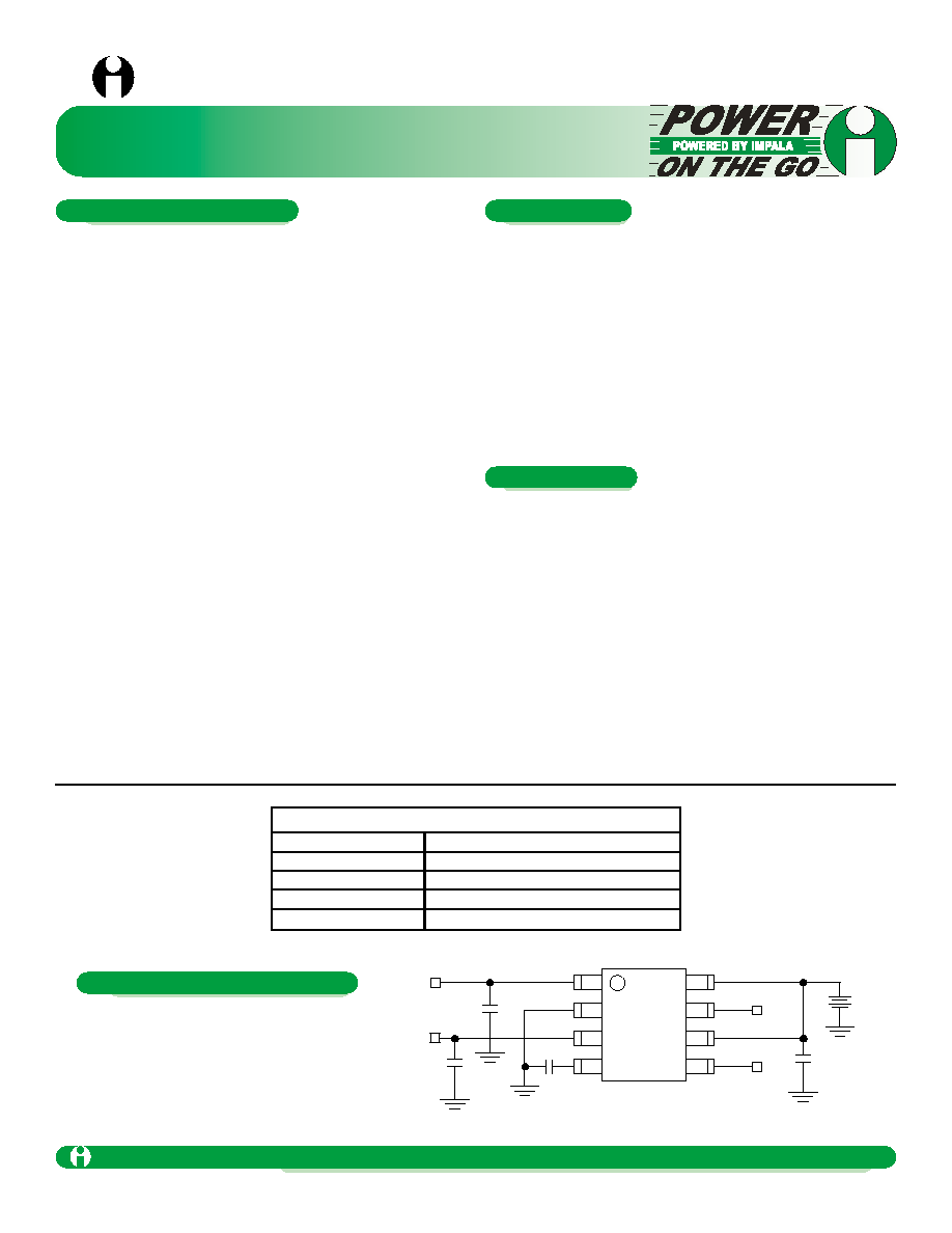
+
+
+
V
INA
V
INB
1µF
ceramic
EN
A
EN
B
GND
C
NOISE
22pF
(optional)
0.47-2.2µF
ceramic
V
OUTA
V
OUTB
0.47-2.2µF
ceramic
4.7µF
+
The ILC7280 is two independent 150mA low dropout (LDO)
voltage regulators in an 8-pin MSOP package. Each regu-
lator output is independently short circuit protected and has
independent enable lines. The device offers a unique com-
bination of low dropout voltage and low quiescent current of
CMOS as well as the low noise and high ripple rejection
characteristics of bipolar LDO regulators. Moreover, only
one input capacitor is required.
Dropout Voltage: Typically 150mV at 150mA load, and
1mV at 1mA load.
Ground pin current: Typically 130µA at 1mA load, and
135µA at 150mA load.
Ripple Rejection: 55dB at 1kHz and 60dB at 100kHz.
Shutdown mode: Less than 0.5µA quiescent current in
shutdown mode.
Small package: MSOP-8
Small capacitor: Requires only a 0.47µF external capacitor
on the regulator output.
Precision output: Output voltage trimmed to 1% accuracy.
Output Noise: 80µV
RMS
, optional noise bypass capacitor
at pin 3 will further reduce noise on V
OUTA/B
Voltage Pairings available: 3.0/3.0V, 3.0/2.8V, 3.0/2.5V,
2.8/2.8V
Micropower Dual 150mA CMOS RF LDOTM Regulators
with 75dB Ripple Rejection
Impala Linear Corporation
Impala Linear Corporation
1
(408) 574-3939
www.impalalinear.com
May 2000
ILC7280 1.8
Advance
∑ Guaranteed 150mA output per regulator
∑ Ultra low 150mV dropout at 150mA
∑ 1% output voltage accuracy
∑ Requires only 0.47µF output capacitor
∑ Only 150µA ground current at 150mA load
∑ 60dB ripple rejection at 1kHz (C
OUT
= 0.47µF)
∑ 80µV
RMS
noise at BW = 300Hz to 50kHz
∑ Excellent line and load transient response
∑ Over current / over temperature protection
∑ 8-pin MSOP package
∑ -60dB cross talk
∑ Cellular Phones, pagers and wireless headsets
∑ Palmtops, organizers, PDAs and portable electronics
∑ Battery powered portable appliances and equipment
∑ Remote data accumulation and instrumentation
General Description
Features
Applications
Figure 1: Typical Application
Note: Enable may be connected to V
IN
,
C
NOISE
is common to both LDOs
ILC7280

Micropower dual 150mA CMOS RF LDOTM Regulators with 75dB Ripple Rejection
Impala Linear Corporation
2
(408) 574-3939
www.impalalinear.com
May 2000
ILC7280 1.8
Advance
Pin Number
1
2
3
4
5
6
7
8
Pin Name
V
OUTA
GND
V
OUTB
C
NOISE (optional)
EN
B
V
INB
EN
A
V
INA
Pin Description
Regulator Output A
Ground
Regulator Output B
Voltage Reference Bypass: Connect external 22pF capacitor to GND to minimize
output noise in regulator "A" or "B." May be left open. Do not ground.
Enable/Shutdown B (input): CMOS compatible input. Logic high = enable, logic low or
open = shutdown. Do not leave floating.
Supply Input B (Internally connected to pin 8)
*
Enable/Shutdown A (Input): CMOS compatible input. Logic high = enable, logic low or
open = shutdown. Do not leave floating.
Supply Input A (Internally connected to pin 6)
*
Galvanic connection only.
C
NOISE(optional)
1
2
3
4
5
6
7
8
V
INA
EN
A
V
INB
EN
B
V
OUTB
GND
V
OUTA
MSOP
(TOP VIEW)
ILC7280CS-XXXX
Pin-Package Configurations
Pin Functions ILC7280
*
If maximum current required from each regulator then connect both pin 6 and pin 8 to V
DD

Micropower Dual 150mA CMOS RF LDOTM Regulators with 75dB Ripple Rejection
Impala Linear Corporation
3
(408) 574-3939
www.impalalinear.com
May 2000
ILC7280 1.8
Advance
Parameter
Input Voltage
S/D Input Voltage
Output Current
Output Voltage
Power Dissipation
Maximum Junction Temperature
Storage Temperature
ESD Rating
Operating Input Voltage
Operating Ambient Temperature
Package Thermal Resistance
Symbol
V
IN
V
S/D
I
OUT
V
OUT
P
D
T
J(max)
T
stg
V
IN
T
A
JA
Ratings
-0.3 to +12
-0.3 to V
IN
Short circuit protected
-0.3 to 10
Internally Limited
175
-40~+125
2
2.1 to 8
-40 to +85
200
Units
V
mA
V
mW
∞C
∞C
kV
V
∞C
∞C/W
Absolute Maximum Ratings (Note 1)

Micropower dual 150mA CMOS RF LDOTM Regulators with 75dB Ripple Rejection
Impala Linear Corporation
4
(408) 574-3939
www.impalalinear.com
May 2000
ILC7280 1.8
Advance
Parameter
Output Voltage
Output Voltage
Output Voltage
Line Regulation
Dropout Voltage (Note 3)
Dropout Voltage (Note 3)
Dropout Voltage (Note 3)
Ground Pin Current
One regulator on
Ground Pin Current
One regulator on
Ground Pin Current
One regulator on
Ground pin Current
Both regulator on
Ground pin Current
Both regulators on
Ground pin Current
Both regulators on
Shutdown Current
Symbol
V
OUT
V
OUT
V
OUT
V
O
/
V
IN
V
IN
- V
OUT
V
IN
- V
OUT
V
IN
- V
OUT
I
GND
I
GND
I
GND
I
GND
I
GND
I
GND
I
S/D
Conditions
I
OUT
= 1mA
1mA < I
OUT
< 100mA
1mA < I
OUT
< 100mA
1mA < I
OUT
< 150mA
1mA < I
OUT
< 150mA
V
O(NOM)
+ 1V < V
IN
< 10V
I
OUT
= 0mA
I
OUT
= 10mA
I
OUT
=150mA
I
OUT
= 0mA
I
OUT
= 10mA
I
OUT
= 150mA
I
OUT
= 0mA
I
OUT
= 10mA
I
OUT
= 150mA
Min
-1
-2
-3
Typ
V
OUT
(Nom.)
V
OUT
(Nom.)
V
OUT
(Nom.)
0.007
0.1
10
150
90
100
135
105
115
150
0.1
Max
+1
+2
+3
0.014
0.032
1
2
15
20
175
200
1
Units
%V
(Nom.)
%V
(Nom.)
%V
(Nom.)
%/V
mV
mV
mV
µA
µA
µA
µA
µA
µA
µA
Electrical Characteristics ILC7280CS
Unless otherwise specified, all limits are at T
A
= 25∞C; V
IN
= V
O(NOM)
+ 1V, I
OUT
= 1mA, C
OUT
= 0.47µF, V
S/D
= 2V.
Boldface limits apply over the operating temperature range. (Note 2)
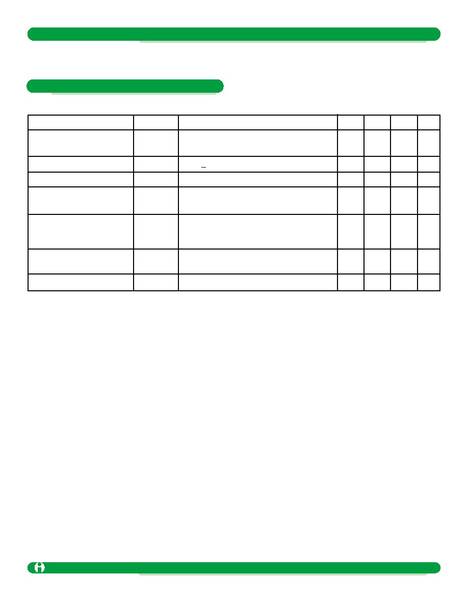
Max
10
0.6
Typ
500
60
60
60
10
40
20
300
Micropower Dual 150mA CMOS RF LDOTM Regulators with 75dB Ripple Rejection
Impala Linear Corporation
5
(408) 574-3939
www.impalalinear.com
May 2000
ILC7280 1.8
Advance
Parameter
Shut Down Input Voltage
Peak Output Current (Note 4)
Output Noise Voltage (RMS)
Ripple Rejection
Dynamic Line Regulation
Dynamic Load Regulation
Short Circuit Current
Symbol
V
S/D
I
O(peak)
e
N
V
O
/
V
IN
V
O(line)
V
O(load)
I
SC
Conditions
High = Regulator On
Low = Regulator Off
V
OUT
> 0.95V
O(NOM)
BW = 300Hz to 50kHz, C
NOISE
= 0pF
freq = 1kHz
freq = 10kHz
freq = 100kHz
V
IN
: V
O(NOM)
+ 1V to V
O(NOM)
+ 2V; dV
IN/dt
=
1V/
µS;lo
= 150mA
I
OUT
: 0 to 150mA; d(l
OUT
)/dt = 50A/µs, with
C
OUT
= 2.2µF
V
OUT
= 0V
Min
2.0
300
Units
V
mA
µV
dB
mV
mV
mA
Electrical Characteristics ILC7280CS
Unless otherwise specified, all limits are at T
A
= 25∞C; V
IN
= V
O(NOM)
+ 1V, I
OUT
= 1mA, C
OUT
= 0.47µF, V
S/D
= 2V.
Boldface limits apply over the operating temperature range. (Note 2)
Note1: Absolute maximum ratings indicate limits which when exceeded may result in damage to the component. Electrical specifications do not apply
when operating the device outside of its rated operating conditions.
Note 2: Specified Min/Max limits are production tested or guaranteed through correlation based on statistical control methods. Measurements are
taken at constant junction temperature as close to ambient as possible using low duty pulse testing.
Note 3: Dropout Voltage is defined as the measured Differential Voltage between input and output voltage, when the output voltage drops 2% below the nominal output
voltage as V
IN
is decreased, and approaches V
OUT
. Nominal output voltage is defined at V
IN
= V
OUT
+ 1V.
Note 4: Guaranteed by design
Micropower Dual 150mA CMOS RF LDOTM Regulators with 75dB Ripple Rejection
Impala Linear Corporation
6
(408) 574-3939
www.impalalinear.com
May 2000
ILC7280 1.8
Advance
CURRENT LIMIT
THERMAL SHUTDOWN
-
+
V
OUTA
EN
A
V
INA
BANDGAP
REF.
V
OUTB
*C
NOISE
EN
B
V
INB
-
+
CURRENT LIMIT
THERMAL SHUTDOWN
GND
*Optional
Micropower Dual 150mA CMOS RF LDOTM Regulators with 75dB Ripple Rejection
Impala Linear Corporation
7
(408) 574-3939
www.impalalinear.com
May 2000
ILC7280 1.8
Advance
Output Capacitor
An output capacitor is required from V
OUTA
and V
OUTB
to
GND to prevent oscillation and minimize the effect of load
transient currents. The minimum size of the output capac-
itor(s) is dependent on the usage of C
NOISE
and its value.
Without C
NOISE
, a minimum of 1µF is recommended. For
C
NOISE
= 22pF, a minimum of 2.2µF is recommended
(See figure 1). Larger values of output capacitance will
slow the regulator's response during power up. The upper
limit of capacitance is indefinite, however, it should have
an equivalent series resistance (ESR) of approximately
5
or less and a series resonance above 1MHz. Stability
is assured with the use of a capacitor having ultra-low
ESR and as such will not produce low amplitude oscilla-
tions nor an underdamped transient response. This
allows the use of modern ceramic capacitors in prefer-
ence to their more costly Tantalum counterparts.
If the system design calls for smaller load currents, lower
capacitance may be used. Below 10mA the capacitance
may be reduced to 0.47µF and below 1mA to 0.33µF.
No-Load Stability
The ILC7280 will remain stable and in regulation with no
load current. These are desirable performance features
for applications such as keep-alive modes in CMOS sys-
tems.
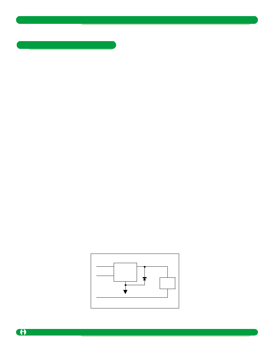
Split-Supply Operation
When using the ILC7280 in a system requiring that the
load be returned to the negative voltage source, the out-
put(s) must be diode clamped to inhibit significant volt-
age excursions below ground. A simple external diode
clamp to ground will afford protection from damage to
the device. (See figure below).
APPLICATIONS INFORMATION
+V
IN
A and B
These pins are connected internally through a galvanic
connection for maximum power from each regulator, both
V
INA
and V
INB
must be connected externally to V
DD
.
Enable/Shutdown
Forcing EN
A
and/or EN
B
to a voltage greater than 2V,
enables the regulator(s). These inputs are CMOS logic
compatible gates. If this feature is not required, connect
EN
A
and/or EN
B
to V
IN
. Note that V
INA
and V
INB
are con-
nected internally. To minimize the effect of imbalanced
current sharing and possible noise, both V
INA
and V
INB
should also be connected externally.
Input Capacitor
A 1µF capacitor should be placed from V
INA/B
to GND if
there is more than 10 inches of wire between the input and
the ac filter capacitor or if a battery is used as the input.
Reference Bypass Capacitor
C
NOISE
(the reference voltage bypass capacitor) is con-
nected to the internal V
ref
which is common to regulator's
A and B. A 22pF capacitor connected between C
NOISE
and
GND decouples the reference output voltage and provides
a significant reduction in regulator output noise. An effect
of C
NOISE
also reduces the regulator phase margin. When
using C
NOISE
, output capacitors of 2.2µF or greater are
required to maintain stability.
Also affected by C
NOISE
is the start up speed of the ICL7280.
The speed is inversely proportional to the value of C
NOISE
. If
a slow or delayed start up time is desired, a larger value of
C
NOISE
is used. Conversely, faster start up times or instant-on
applications will require smaller values of C
NOISE
or its omis-
sion with the pin left open. The trade-off of noise to response
should be considered.
+V
IN
EN
A
/EN
B
-V
IN
ILC7280
Dual Regulator
V
OUTA
or V
OUTB
Dext
Rload
External Diode, Dext inhibits significant voltage excursions
below ground in a split power supply load return.

Micropower Dual 150mA CMOS RF LDOTM Regulators with 75dB Ripple Rejection
Impala Linear Corporation
8
(408) 574-3939
www.impalalinear.com
May 2000
ILC7280 1.8
Advance
Thermal Considerations
For optimum Thermal dissipation and device reliability,
devices mounted on conventional FR4 PCB material
should be surrounded and connected to as much ground
copper as possible. In a worse case application with min-
imum trace widths and no ground plane, the MSOP-8
package exhibits a thermal resistance of 200 ∞C/W. The
risk to the device can be calculated in the following exam-
ples. (An Excel spreadsheet calculator is also available at
the Impala Linear web site: Products/ILC7280.)
Thermal Evaluation Examples
For an ambient temperature of 50∞C, the maximum pack-
age power dissipation is:
P D(max) = (125∞C - 50∞C) / 200∞C/W
P D(max) = 375mW
If the intent is to operate from a 4V power source with a
150mA load current from both outputs at a 50∞C ambient
temperature, the expected power dissipation is found in
the following calculation:
P D(each regulator) = (V
IN
- V
OUT
) * I
OUT
+ (V
IN
* I
GND
)
P D(each regulator) = (4V - 3V) * 150mA + (4V * 0.12mA)
P D(each regulator) = 150mW
P D(both regulators) = 2 * 150mW
P D(both regulators) = 300mW
In this example the total power dissipated is 300mW which
is below the 375mW maximum package consideration and
therefore safe to operate. It should be noted that it is not
always possible to operate both regulators at the maximum
output current. For example in a 5V input and 3V output
application at 50∞C, one regulator operating at 150ma
would dissipate 267.5mW. The remaining regulator must
be limited to 375mW - 267.5mW or 107.5mW.
An advantage of the ILC7280 low-dropout voltage charac-
teristic is that using the lowest possible input voltage can
minimize power dissipation.
APPLICATIONS INFORMATION cont.
Micropower Dual 150mA CMOS RF LDOTM Regulators with 75dB Ripple Rejection
Impala Linear Corporation
9
(408) 574-3939
www.impalalinear.com
May 2000
ILC7280 1.8
Advance
Devices sold by Impala Linear Corporation are covered by the warranty and patent indemnification provisions appearing
in its Terms of Sale only. Impala Linear Corporation makes no warranty, express, statutory, implied, or by description
regarding the information set forth herein or regarding the freedom of the described devices from patent infringement.
Impala Linear Corporation makes no warranty of merchantability or fitness for any purpose. Impala Linear Corporation
reserves the right to discontinue production and change specifications and prices at any time and without notice.
This product is intended for use in normal commercial applications. Applications requiring an extended temperature
range, unusual environmental requirements, or high reliability applications, such as military and aerospace, are specif-
ically not recommended without additional processing by Impala Linear Corporation.
Impala Linear Corporation assumes no responsibility for the use of any circuitry other than circuitry embodied in an
Impala Linear Corporation product. No other circuits, patents, licenses are implied.
Life Support Policy
Impala Linear Corporation's products are not authorized for use as critical components in life support devices or systems.
1. Life support devices or systems are devices or systems which, (a) are intended for surgical implant into the body, or
(b) support or sustain life, and whose failure to perform, when properly used in accordance with instructions for use pro-
vided in the labeling, can be reasonably expected to result in a significant injury to the user.
2. A critical component is any component of a life support device or system whose failure to perform can be reason-
ably expected to cause the failure of the life support device or system, or to affect its safety or effectiveness.
0.0215
0.037
3 TYP
0.006 RAD. TYP
0.116
12 TYP
12 TYP
0.118
0.000-0.005 RAD. TYP
0.040
0.004
SEATING PLANE
0.118 ± 0.004
0.020 TYP
0.013 TYP
0.0256 BSC
0.118 ± 0.004
All dimensions in inches
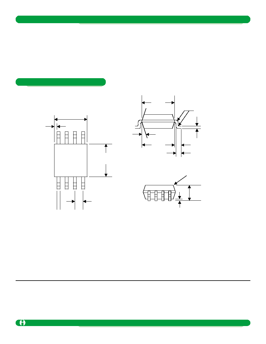
Package Dimensions
MSOP-8