 | –≠–ª–µ–∫—Ç—Ä–æ–Ω–Ω—ã–π –∫–æ–º–ø–æ–Ω–µ–Ω—Ç: ILC7526 | –°–∫–∞—á–∞—Ç—å:  PDF PDF  ZIP ZIP |
∑ 2 independent switches with ENABLE and FLAG
∑ 500mA continuous load current per switch (channel)
∑ 140m
maximum R
DSON
(switch on-resistance)
∑ 1.25A maximum short circuit current limit
∑ Thermal shutdown
∑ 110µA typical on-state supply current
∑ 0.75µA typical off-state supply current
∑ 2.4V typical undervoltage lockout
∑ 2.8V to 5.8V input voltage range
∑ 1 ms turn-on (soft-start)
∑ Fast turn-off
∑ Outputs can be forced higher than inputs (off-state)
∑ USB specification compliant
∑ Active-high or active-low ENABLE versions
∑ 8-pin SOIC or 8-pin mini-DIP packages
∑ USB host and self powered hubs
∑ USB bus-powered hubs
∑ USB monitors, printers, cameras and other USB
controlled peripherals
∑ Hot plug-in power supplies
∑ Battery charger circuits
The ILC7526 contains dual high side power control
switches, with independent enable and flag functions,
integrated into a single 8-pin SOIC package. With just a
few external components, the ILC7526 can be easily con-
figured to meet requirements for either self powered or
bus powered USB (Universal Serial Bus) applications.
The ILC7526 has active high ENABLE inputs, while the
ILC7536 ENABLE inputs are active low.
With a maximum R
DSON
value of 140m
per switch, the
USB voltage drop requirements can be achieved. Each
switch can also supply up to 500mA, with internal circuitry
limiting the fault current to 750mA. Fault conditions are also
reported to the USB controller via one of the independent
flag pins. Internal circuitry provides a soft-start that elimi-
nates momentary upstream voltage drops when the switch
is enabled, especially in bus powered applications.
Additional features include undervoltage lockout (2.4V),
fast turn-off, 2.8V to 5.8V input voltage range, thermal
shutdown to prevent switch failure from high current loads,
and 3.3V and 5V logic compatible enable inputs.
The ILC7526 and ILC7536 are available in both 8-pin SOIC
and 8-pin mini-DIP packages.
ILC7526/7536
USB Dual Control Switches
Impala Linear Corporation
Impala Linear Corporation
1
(408) 574-3939
www.impalalinear.com
Dec 2000
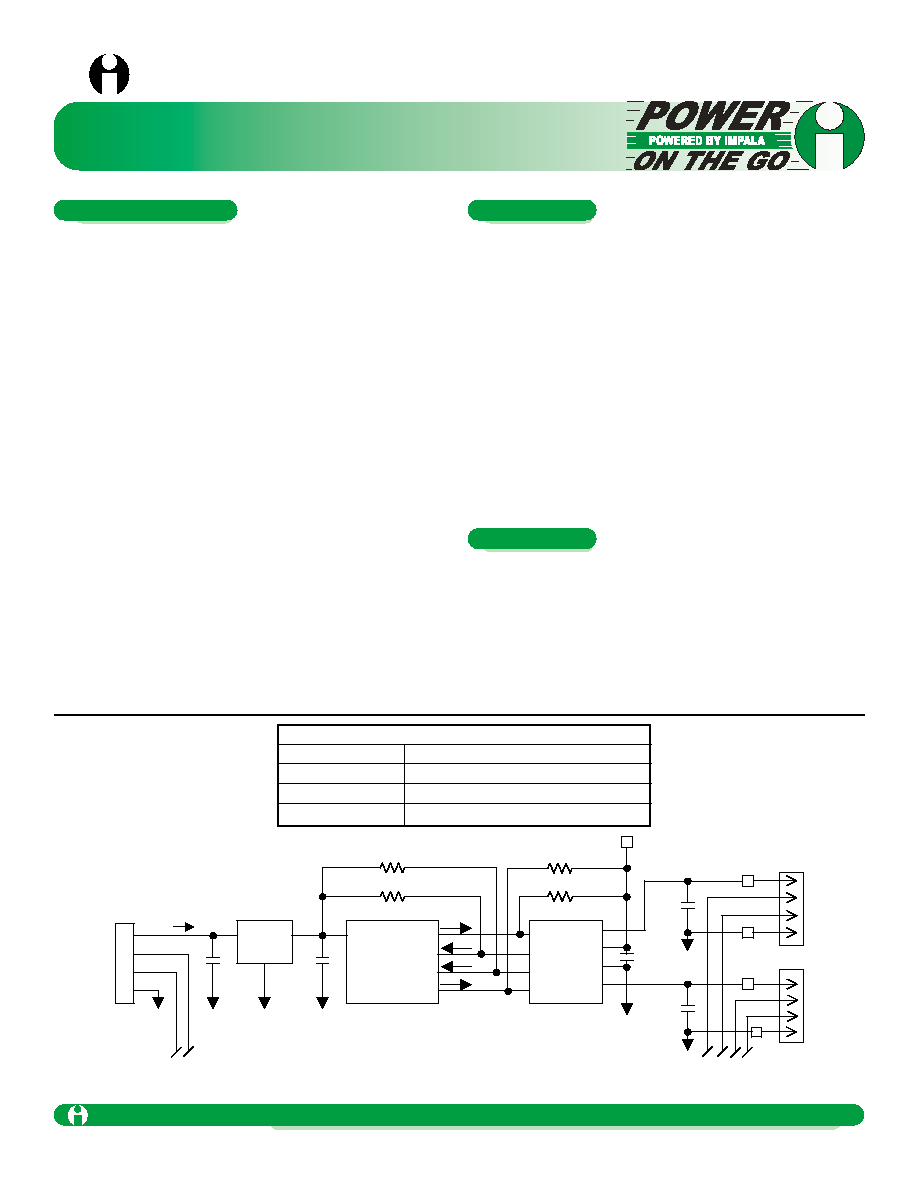
ILC7526/7536 1.5
Final
V
BUS
4.5V to 5.25V
Upstream VBUS
100mA max
D+
D-
GND
Data
ILC7082-3.3
IN
1µF
GND
3.3V USB Controller
100k
100k
1µF
ON/OFF
V
IN
OVERCURRENT
OVERCURRENT
ON/OFF
ENA
FLGA
FLGB
ENB
IN
GND
OUTB
ILC7526
V
CC
5.0V
+
+
47µF
0.1µF
47µF
V
BUS
D+
D-
GND
V
BUS
D+
D-
GND
Data
(Two Pair)
to USB Controller
100k
100k
OUTA
OUT
Ordering Information* (T
A
= -40∞C to =85∞C)
ILC7526-IK
ILC7526-IN
ILC7536-IK
ILC7536-IN
Active High Enable, SO-8 package
Active High, DIP-8 package
Active Low, SO-8 package
Active Low, DIP-8 package
General Description
Features
Applications
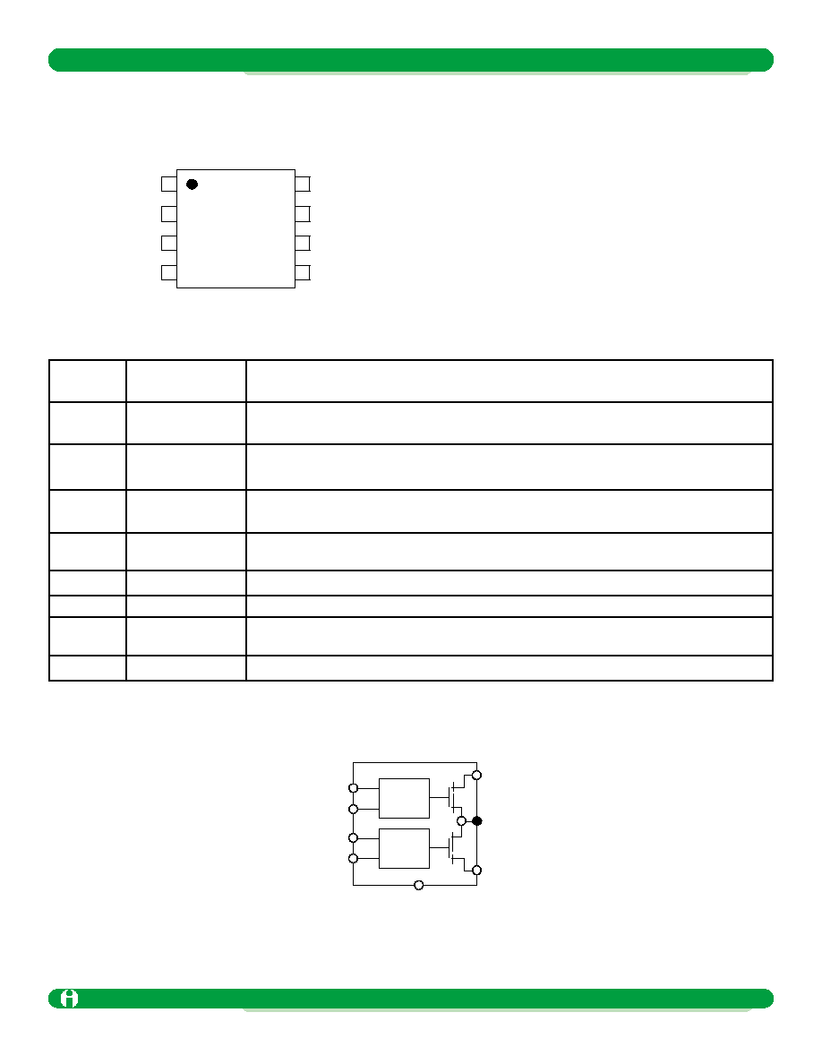
Pin Name
ENA
FLGA
FLGB
ENB
OUTB
GND
IN
OUTA
Pin Description
Enable A (input): Logic-compatible enable input. (7526 active-high, 7536 active-low).
Do not float.
Fault Flag A (Output): Active-low, open-drain output. Indicates overcurrent, UVLO,
or thermal shutdown.
Fault Flag B (Output): Active-low, open-drain output. Indicates overcurrent, UVLO,
or thermal shutdown.
Enable B (Input): Logic-compatible enable input. (7526 active-high, 7536 active-low).
Do not float.
Switch Output B: Output MOSFET source. Typically connect to switched side of load.
Ground: Supply return.
Supply Input: Output MOSFET drain. Also supplies IC's internal circuitry.
Connect to positive supply.
Switch Output A: Output MOSFET source. Typically connect to switched side of load.
Pin
Number
1
2
3
4
5
6
7
8
USB Dual Control Switches
Impala Linear Corporation
2
(408) 574-3939
www.impalalinear.com
Dec 2000
ILC7526/7536 1.5
Preliminary
(FLGB)3
(FLGA)2
(ENA)1
(ENB)4
(OUTA)8
(IN)7
(OUTB)5
LOGIC
CHARGE
PUMP
LOGIC
CHARGE
PUMP
ILC7526
(GND)6
FLGB
ENA
FLGA
ENB
OUTA
IN
GND
OUTB
1
2
3
4
8
7
6
5
Figure 2: Pin Configuration
USB Dual Control Switches
Impala Linear Corporation
3
(408) 574-3939
www.impalalinear.com
Dec 2000
ILC7526/7536 1.5
Preliminary
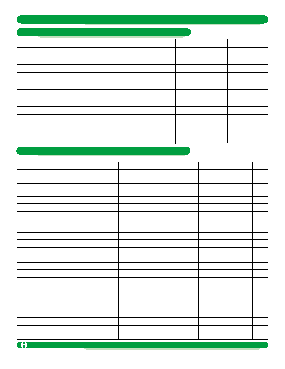
Conditions
Switch off, OUT = Open
All switches on, OUT = Open
Low to high transition
High to low transition (Note 3)
V
EN
= 0V to 5.8V
V
IN
= 5V, I
OUT
= 500mA each switch
V
IN
= 3.3V, I
OUT
= 500mA each switch
R
L
= 10
each output
R
L
= 10
each output
R
L
= 10
each output
R
L
= 10
each output
Output disabled, each output
Each output
ENABLE into load, V
OUT
= 4.0V
Ramped load to enabled output
V
OUT
< 4.0V, Note 2
T
J
(Junction temperature) increasing
T
J
(Junction temperature) decreasing
V
IN
= 5V, I
L
= 10mA
V
IN
= 3.3V, I
L
= 10mA
V
FLG
= 5V
V
IN
= increasing
V
IN
= decreasing
Ratings
+6
+6
50
+6
Internally Limited
-0.3 to +12
-40 to +125
-40 to +85
120
130
260
Parameter
Input Supply Voltage
Fault Flag Voltage
Fault Flag Current
Output Voltage
Output Current
ENABLE Input Voltage
Storage Temperature
Operating Ambient Temperature
Package Thermal Resistance
SOIC 8-Pin
DIP
Lead Temperature (soldering 5 sec)
Symbol
V
IN
V
FLG
I
FLG
V
OUT
I
OUT
V
EN
T
STG
T
A
JA
JA
Units
V
V
mA
V
mA
V
∞C
∞C
∞C/W
∞C/W
∞C
Parameter
Supply Current
ENABLE Input Threshold
ENABLE Input Current
ENABLE Input Capacitance
Switch resistance
Output Turn-on Delay
Output Turn-on Rise Time
Output Turn-off Delay
Output Turn-off Fall Time
Output Leakage Current
Continuous Load Current
Short Circuit Current Limit
Current Limit Threshold
Over Temperature Shutdown
Threshold
Error Flag Output Resistance
Error Flag Off Current
Under Voltage Lockout Threshold
Symbol
I
SS
V
ENTH
I
EN
C
EN
R
DSON
T
ON
T
OR
T
OFD
T
OFF
I
OL
I
OUT
I
SCL
I
LTH
O
TTH
R
FLG
I
FLG
UVLO
Min
0.8
-1
0.5
0.5
Typ
0.75
110
2.1
1.9
+0.01
1
100
140
0.5
1
1
1
0.75
1.6
135
125
10
15
0.01
2.5
2.3
Units
µA
µA
V
V
µA
pF
m
m
ms
ms
µs
µs
µA
A
A
A
∞C
∞C
µA
V
Max
2.4
1
140
180
20
20
10
1.25
2.2
25
40
1
Absolute Maximum Ratings
(Note 1, notes on next page)
Electrical Characteristics ILC7526IK
Test circuit shown in Fig. 2. BOLDFACE type indicates limits that apply over the full operating temperature range (Note 2).
USB Dual Control Switches
Impala Linear Corporation
4
(408) 574-3939
www.impalalinear.com
Dec 2000
ILC7526/7536 1.5
Preliminary
Note 1. Stresses above those listed under ABSOLUTE MAXIMUM RAT-
INGS may cause permanent device failure. Functionality at or above
these limits is not implied. Exposure to absolute maximum ratings for
extended periods may affect device reliability. Operating ranges define
those limits between which the functionality of the device is guaranteed.
Note 2. Specified min/max limits are production tested or guaranteed
through correlation based on statistical control methods. Measurements
are taken at constant junction temperature as close to ambient as possible
using low duty pulse testing.
Note 3. Off is < 0.8V and On is > 2.4V for the ILC7526. Off is > 2.4V for
the ILC7536. The enable input has approximately 200mV of hysteresis.
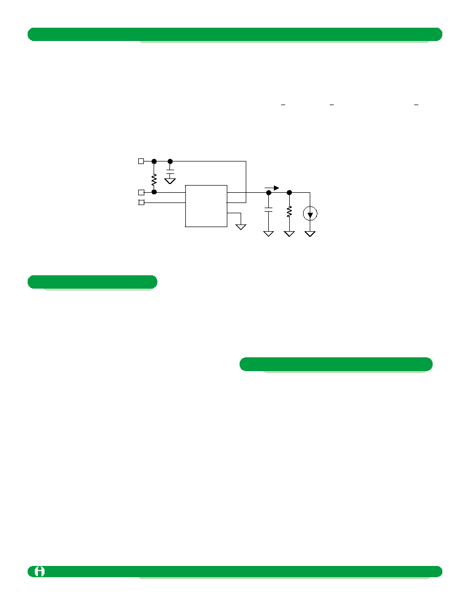
ILC7526
5V
10k
0.1µF
ENA
FLGA
FLGB
ENB
OUTA
IN
GND
OutB
I
OUT
C
L
+
R
L
(1 output shown)
The ILC7526 and ILC7536 are dual high-side switches with
active-high and active-low enable inputs, respectively.
Fault conditions turn-off or inhibit turn-on of one or more of
the output transistors, depending upon the type of fault,
and also activate the open-drain error flag transistors
which sink current to ground.
Input and Output
IN (input) is the power supply connection to the logic circuit-
ry and the drains of both of the output MOSFET's. OUTx
(output) is the source of each MOSFET. In a typical circuit,
current flows through the switch from IN to OUT toward the
load. If V
OUT
is greater than V
IN
when a switch is enabled,
current will flow from OUT to IN since the MOSFET is bidi-
rectional when on.
The output MOSFET and driver circuitry are also designed to
allow the MOSFET source to be externally forced to a higher
voltage than the drain (V
OUT
> V
IN
) when the output is off. In
this situation, the ILC7526 avoids undesirable current flow
from OUT to IN. If V
IN
< 2.5V, UVLO disables both switches.
Thermal Shutdown
Thermal shutdown shuts off the affected output MOSFET's
and signals all fault flags if the die temperature exceeds
135∞C. 10∞C of hysteresis prevents the switch from turn-
ing on until the die temperature drops to 125∞C.
Overtemperature detection functions only when at least
one switch is enabled.
Internal circuitry increases the output MOSFET on-resist-
ance until the series combination of the MOSFET on-resist-
ance and the load impedance limit current to typically
850mA. The increase in power dissipation, in most cases,
will cause the ILC7526 to go into thermal shutdown, dis-
abling affected channels. When this is undesirable, thermal
shutdown can be avoided by externally responding to the
fault and disabling the current limited channel before the
shutdown temperature is reached. The delay between the
flag indication of a current limit fault and thermal shutdown
will vary with ambient temperature, board layout, and load
impedance, but is typically several hundred milliseconds.
The USB controller must therefore recognize a fault and
disable the appropriate channel within this time. If the fault
is not removed or the switch is not disabled within this time,
the device will enter into a thermal oscillation of about 2Hz.
This does not cause any damage to the device.
Functional Description
Current Limit Induced Thermal Shutdown
USB Dual Control Switches
Impala Linear Corporation
5
(408) 574-3939
www.impalalinear.com
Dec 2000
ILC75267536 1.5
Preliminary
Undervoltage Lockout
UVLO (undervoltage lockout) prevents the output MOS-
FET from turning on until V
IN
exceeds approximately 2.5V.
In the undervoltage state, the FLAG will be low. After the
switch turns on, if the voltage drops below approximately
2.3V, UVLO shuts off the output MOSFET and signals fault
flag. Undervoltage detection functions only when at least
one switch is enabled.
Current Sensing and Limiting
The current-limit threshold is preset internally. The pre-
set level prevents damage to the output MOSFET and
external load but allows a minimum current of 0.5A
through the output MOSFET of each channel. The cur-
rent-limit circuit senses a portion of the output FET
switch current. The reaction to an overcurrent condition
varies with three scenarios:
Switch Enabled into Short Circuit
If a switch is powered on or enabled into a heavy load or
short circuit, the switch immediately goes into a constant-
current mode, reducing the output voltage. The fault flag
goes low until the load is reduced.
Short Circuit Applied to Output
When a heavy load is applied, a large transient current may
flow until the current limit circuitry will respond. Once this
occurs, the device limits current to less than the short-circuit
current limit specification.
Current-Limit Response
The ILC7526 current-limit profile exhibits a small foldback
effect of approximately 500mA. Once this current-limit
threshold is exceeded the device enters constant-current
mode. This constant current is specified as the short circuit
current limit in the "Electrical Characteristics" table. it is
important to note that the device will deliver load current up
to the current-limit threshold which is typically 1.6A
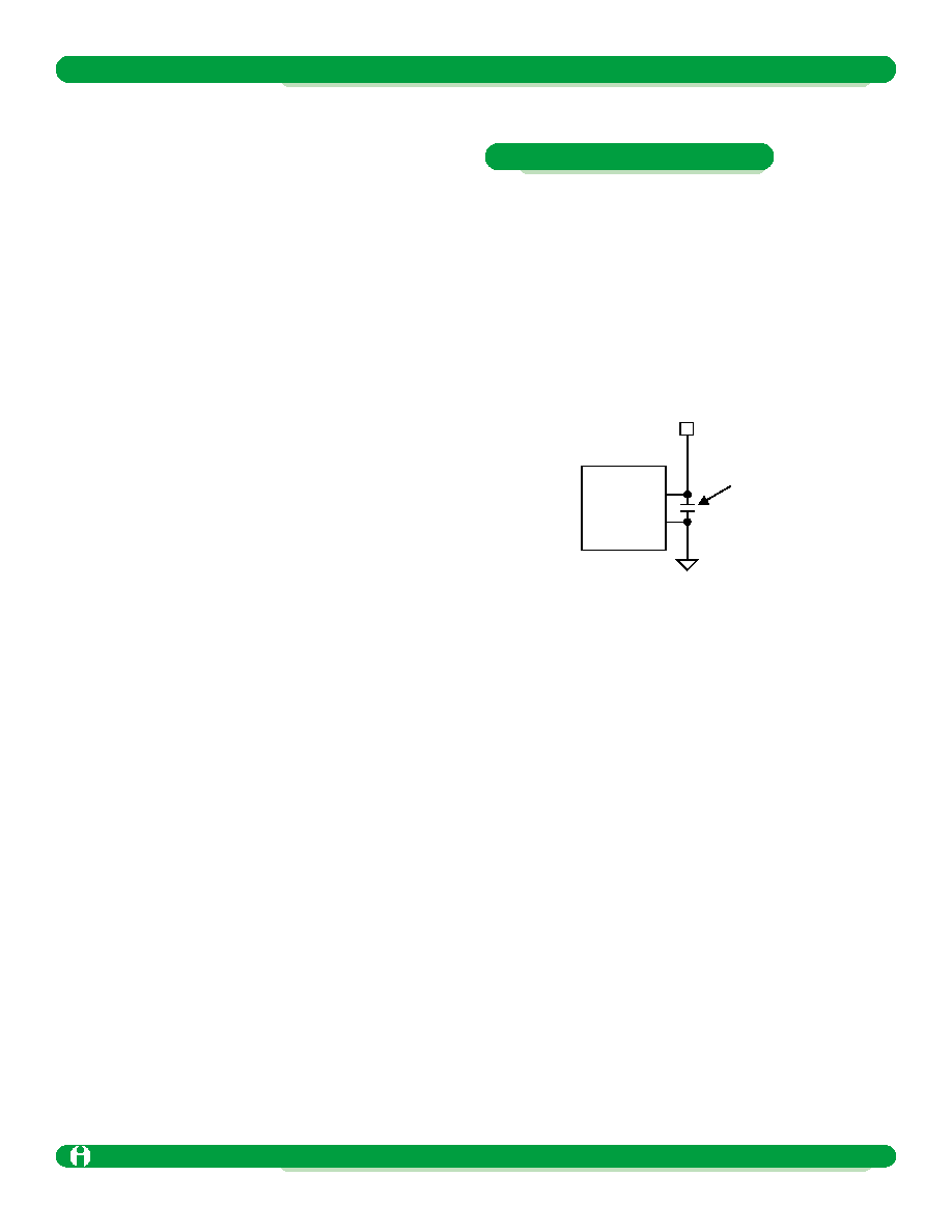
Fault Flag
FLG is an N-channel, open-drain MOSFET output. The fault-
flag is active (low) for one or more of the following conditions:
undervoltage (while 2V < V
IN
< 2.7), current limit, or thermal
shutdown. The flag output MOSFET is capable of sinking a
10mA load to typically 100mV above ground. Multiple FLG
pins may be wired "NORed" to a common pull-up resistor.
Enable Input
EN must be driven logic high or logic low for a clearly
defined input. Floating the input may cause unpre-
dictable operation. EN should not be allowed to go neg-
ative with respect to GND.
Soft-Start
The ILC7526 presents a high impedance when off, and
slowly becomes a low impedance as it turns on. This
reduces in rush current and related voltage drop that
results from charging a capacitive load, satisfying the USB
voltage drop requirements for bus-powered applications.
ILC7526
ENA
FLGA
FLGB
ENB
OUTA
IN
GND
OutB
0.1µF to 1µF
3.0V to 5.5V
A
PPLICATIONS
I
NFORMATION
Supply Filtering
A 0.1µF to 1µF bypass capacitor from IN to GND, located at
the device, is strongly recommended to control supply tran-
sients. Without a bypass capacitor, an output short may
cause sufficient ringing on the input (from supply lead induc-
tance) to damage internal control circuitry. Input or output
transients must not exceed the absolute maximum output
supply voltage (V
IN MAX
= 6V) even for a short duration.