Data Sheet
1
2004-04-05
PTF080901E
Package 30248
-90
-80
-70
-60
-50
-40
-30
-20
-10
0
36
38
40
42
44
46
48
50
Output Power (dBm)
Modula
t
ion Spec
trum (dB)
10
15
20
25
30
35
40
45
50
55
Drain Efficiency (%)
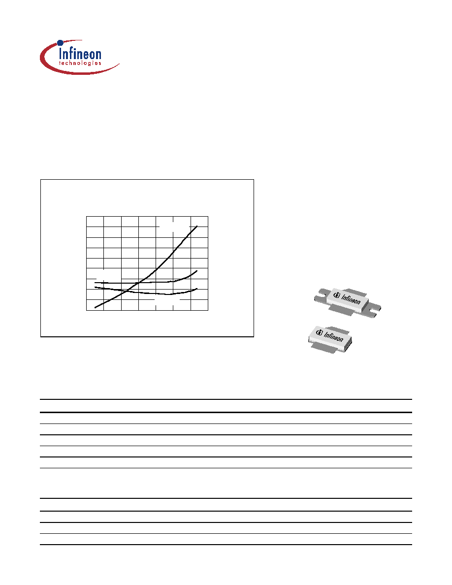
EDGE Modulation Spectrum Performance
V
DD
= 28 V, I
DQ
= 700 mA, f = 959.8 MHz
Efficiency
400 kHz
600 kHz
PTF080901
LDMOS RF Power Field Effect Transistor
90 W, 869≠960 MHz
Features
∑ Broadband internal matching
∑ Typical EDGE performance
- Average output power = 45 W
- Gain = 18 dB
- Efficiency = 40%
∑ Typical CW performance
- Output power at P≠1dB = 120 W
- Gain = 17 dB
- Efficiency = 60%
∑ Integrated ESD protection: Human Body
Model, Class 1 (minimum)
∑ Excellent thermal stability
∑ Low HCI drift
∑ Capable of handling 10:1 VSWR @ 28 V,
90 W (CW) output power
ESD: Electrostatic discharge sensitive device--observe handling precautions!
Description
The PTF080901 is a 90 W, internally matched GOLDMOS FET intended
for EDGE and CDMA applications in the 860 to 960 MHz band. Full gold
metallization ensures excellent device lifetime and reliability.
RF Characteristics
at T
CASE
= 25∞C unless otherwise indicated
EDGE Measurements
(not subject to production test--verified by design/characterization in Infineon test fixture)
V
DD
= 28 V, I
DQ
= 700 mA, P
OUT
= 45 W, f = 959.8 MHz
Characteristic
Symbol
Min
Typ
Max
Unit
Error Vector Magnitude
EVM (RMS)
--
2.5
--
%
Modulation Spectrum @ 400 kHz
ACPR
--
≠62
--
dBc
Modulation Spectrum @ 600 kHz
ACPR
--
≠74
--
dBc
Gain
G
ps
--
18
--
dB
Drain Efficiency
D
--
40
--
%
Two≠Tone Measurements
(tested in Infineon test fixture)
V
DD
= 28 V, I
DQ
= 650 mA, P
OUT
= 90 W PEP, f = 960 MHz, tone spacing = 1 MHz
Characteristic
Symbol
Min
Typ
Max
Unit
Gain
G
ps
17
18
--
dB
Drain Efficiency
D
40
42
--
%
Intermodulation Distortion
IMD
--
≠32
≠29
dBc
PTF080901F
Package 31248
Data Sheet
2
2004-04-05
PTF080901
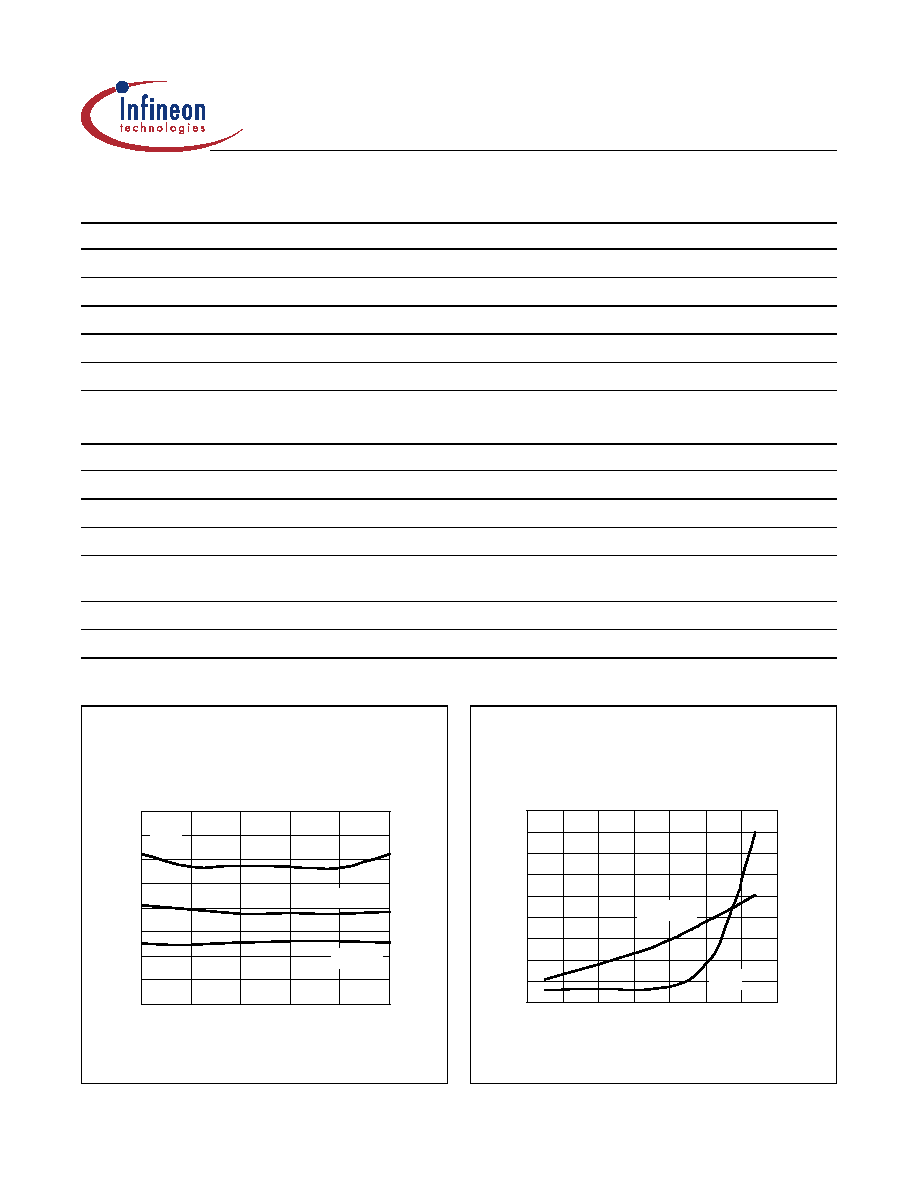
Typical Performance
(measurements taken in production test fixture)
Modulation Spectrum
P
OUT
= 40 W, f = 959.8 MHz
0.5
0.7
0.9
1.1
1.3
1.5
1.7
1.9
2.1
0.47
0.57
0.67
0.77
0.87
0.97
Quiescent Current (A)
EVM RMS (average %)
.
-100
-90
-80
-70
-60
-50
-40
-30
-20
Modula
t
ion Spec
trum (dBc)
EVM
400 KHz
600 KHz
0
1
2
3
4
5
6
7
8
9
36
38
40
42
44
46
48
50
Output Power (dBm)
EVM RMS (average %)
.
0
10
20
30
40
50
60
70
80
90
Drain Efficiency (%)
EDGE EVM Performance
V
DD
= 28 V, I
DQ
= 700 mA, f = 959.8 MHz
EVM
Efficiency
DC Characteristics
at T
CASE
= 25∞C unless otherwise indicated
Characteristic
Conditions
Symbol
Min
Typ
Max
Unit
Drain≠Source Breakdown Voltage
V
GS
= 0 V, I
DS
= 10 µA
V
(BR)DSS
65
--
--
V
Drain Leakage Current
V
DS
= 28 V, V
GS
= 0 V
I
DSS
--
--
1.0
µA
On≠State Resistance
V
GS
= 10 V, V
DS
= 0.1 V
R
DS(on)
--
0.1
--
V
Operating Gate Voltage
V
DS
= 28 V, I
DQ
= 650 mA
V
GS
2.5
3.2
4
V
Gate Leakage Current
V
GS
= 10 V, V
DS
= 0 V
I
GSS
--
--
1.0
µA
Maximum Ratings
Parameter
Symbol
Value
Unit
Drain≠Source Voltage
V
DSS
65
V
Gate≠Source Voltage
V
GS
≠0.5 to +12
V
Junction Temperature
T
J
200
∞C
Total Device Dissipation
P
D
335
W
Above 25∞C derate by
1.9
W/∞C
Storage Temperature Range
T
STG
≠40 to +150
∞C
Thermal Resistance (T
CASE
= 70∞C)
R
JC
0.52
∞C/W
All published data at T
CASE
= 25∞C unless otherwise indicated.
Data Sheet
3
2004-04-05
PTF080901
-80
-70
-60
-50
-40
-30
-20
-10
0
43
45
47
49
51
Output Power (dBm), PEP
IMD (dBc)
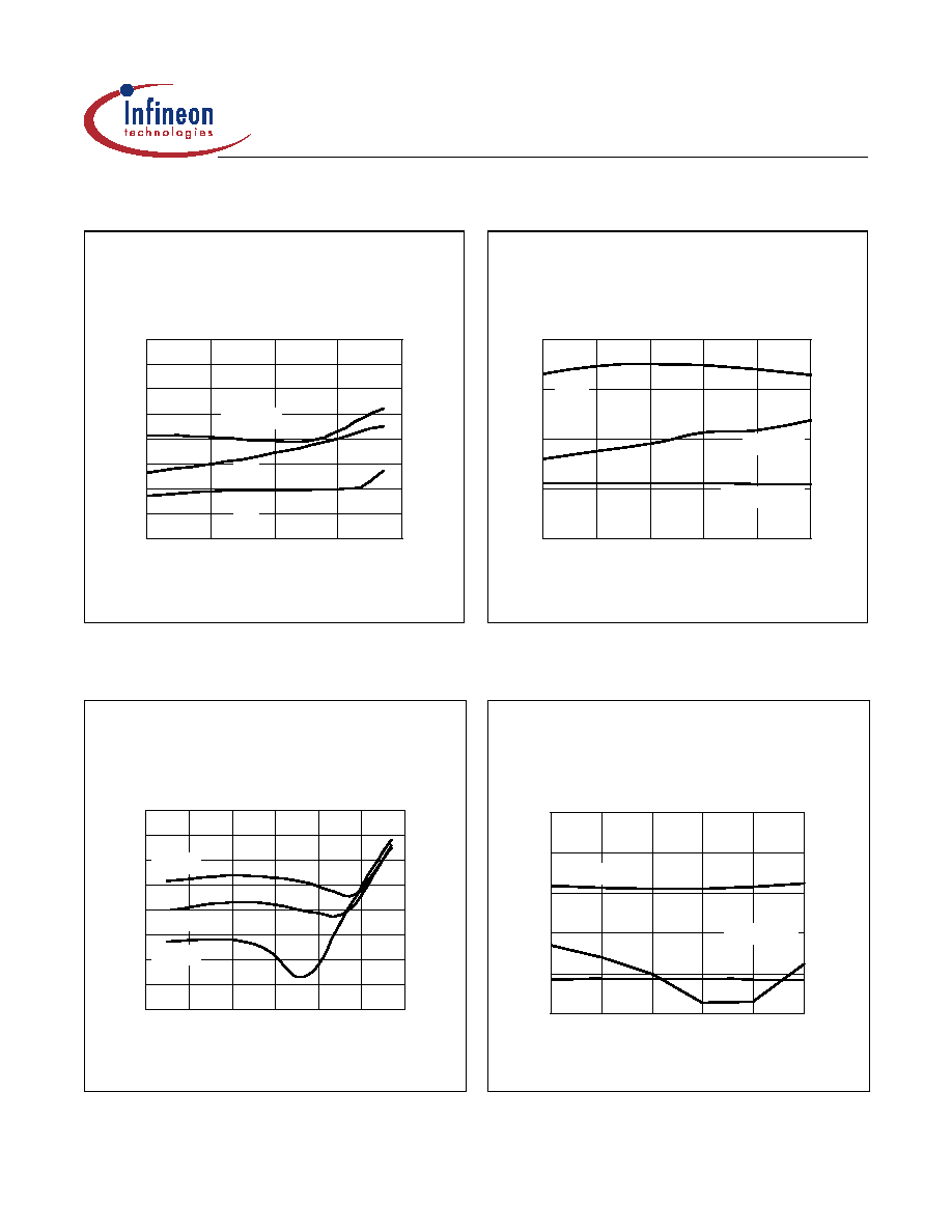
Intermodulation Distortion vs. Output Power
(as measured in a broadband circuit)
V
DD
= 28 V, I
DQ
= 650 mA, f
1
= 959 MHz, f
2
= 960 MHz
3rd Order
7th
5th
14
15
16
17
18
860
880
900
920
940
960
Frequency (MHz)
Gain (dB)
40
50
60
70
80
Efficiency (%), P
OUT
(dBm)
Output Pow er
Efficiency
Gain
Typical P
OUT
, Gain & Efficiency
(at P-1dB)
vs. Frequency
V
DD
= 28 V, I
DQ
= 650 mA
Typical Performance
(cont.)
All published data at T
CASE
= 25∞C unless otherwise indicated.
IM3 vs. Output Power at Selected Biases
V
DD
= 28 V, f
1
= 959, f
2
= 960 MHz
-60
-55
-50
-45
-40
-35
-30
-25
-20
39
41
43
45
47
49
51
Output Power (dBm), PEP
IMD (dBc)
480 mA
820 mA
650 mA
Broadband Performance
V
DD
= 28 V, I
DQ
= 650 mA, P
OUT
= 45 W
10
20
30
40
50
60
860
880
900
920
940
960
Frequency (MHz)
Gain (dB), Efficiency (%)
-15
-12
-9
-6
-3
0
Return Loss (dB)
Gain
Return Loss
Efficiency

Series show current.
PTF080901
Typical Performance
(cont.)
Three≠Carrier CDMA 2000 Performance
V
DD
= 28 V, I
DQ
= 700 mA, f = 880 MHz
15
20
25
30
35
40
45
50
39
40
41
42
43
44
45
Output Power (dBm), Avg.
Drain Efficiency (%)
-65
-62
-59
-56
-53
-50
-47
-44
Adjacen
t Channel
Power Ratio (dBc)
Efficiency
ALT Up
ACP Low
ACP Up
Bias Voltage vs. Temperature
Voltage normalized to typical gate voltage.
0.96
0.97
0.98
0.99
1.00
1.01
1.02
1.03
-20
0
20
40
60
80
100
Case Temperature (∫C)
Nor
malized
Bias Voltage
1.50 A
3.00 A
4.50 A
6.00 A
7.50 A
9.00 A
All published data at T
CASE
= 25∞C unless otherwise indicated.
Broadband Circuit Impedance
0
.
1
0
.
2
0.1
0.1
-
W
A
V
E
L
E
N
G
T
H
S
T
O
W
A
R
D
G
E
N
E
--
-W
A
V
E
L
E
N
G
T
H
S
T
O
W
A
R
D
L
O
A
D
-
0
.
0
860 MHz
860 MHz
980 MHz
980 MHz
Z Load
Z Source
Z
0
= 50
Frequency
Z Source
Z Load
MHz
R
jX
R
jX
860
2.50
≠1.09
1.98
≠1.08
920
2.67
≠0.43
1.99
≠0.32
940
2.79
≠0.35
1.87
≠0.21
960
2.94
0.12
1.85
0.27
980
2.91
0.37
1.79
0.53
Z Source
Z Load
G
S
D
Data Sheet
5
2004-04-05
