Aug-28-2001
1
BAR64-04S
VPS05604
6
3
1
5
4
2
Silicon PIN Diode
Preliminary data
High voltage current controlled
RF resistor for RF attenuator and switches
Frequency range above 1MHz up to 3 GHz
Low resistance and long carrier life time
Very low capacitance at zero volts reverse
bias at frequencies above 1 GHz
Very low signal distortion
EHA07464
6
5
4
3
2
1
C1/A2
C3
A4
A3/C4
C2
A1
D1
D4
D2
D3
Type
Marking
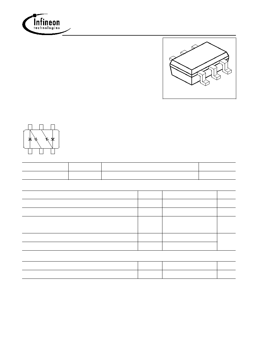
Pin Configuration
Package
BAR64-04S
PPs
For pin configuration see figure above
SOT363
Maximum Ratings
Parameter
Symbol
Value
Unit
Diode reverse voltage
V
R
150
V
Forward current
I
F
100
mA
Total power dissipation
T
S
= tbd
P
tot
tbd
mW
Operating temperature range
T
op
-55 ... 125
∞C
Storage temperature
T
stg
-55 ... 150
Thermal Resistance
Parameter
Symbol
Value
Unit
Junction - soldering point
1)
R
thJS
tbd
K/W
1
For calculation of R
thJA
please refer to Application Note Thermal Resistance

Aug-28-2001
2
BAR64-04S
Electrical Characteristics at T
A
= 25∞C, unless otherwise specified
Parameter
Symbol
Values
Unit
min.
typ.
max.
DC Characteristics
Breakdown voltage
I
(BR)
= 5 µA
V
(BR)
150
-
-
V
Forward voltage
I
F
= 50 mA
V
F
-
-
1.1
AC Characteristics
Diode capacitance-
V
R
= 20 V, f = 1 MHz
C
T
-
0.23
0.35
pF
Forward resistance
I
F
= 1 mA, f = 100 MHz
I
F
= 10 mA, f = 100 MHz
I
F
= 100 mA, f = 100 MHz
r
f
-
-
-
12.5
2.1
0.85
20
3.8
1.35
Charge carrier life time
I
F
= 10 mA, I
R
= 6 mA, I
R
= 3 mA
rr
-
1.55
-
µs
Case capacitance
f
= 1 MHz
C
C
-
0.09
-
pF
Series inductance
L
S
-
0.6
-
nH
