 | –≠–ª–µ–∫—Ç—Ä–æ–Ω–Ω—ã–π –∫–æ–º–ø–æ–Ω–µ–Ω—Ç: BCP29 | –°–∫–∞—á–∞—Ç—å:  PDF PDF  ZIP ZIP |
BCP29, BCP49
1
Nov-29-2001
NPN Silicon Darlington Transistors
For general AF applications
High collector current
High current gain
Complementary types: BCP28/48 (PNP)
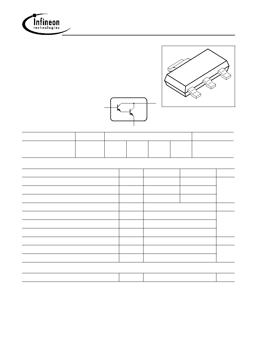
VPS05163
1
2
3
4
EHA00009
B(1)
E(3)
C(2,4)
Type
Marking
Pin Configuration
Package
BCP29
BCP49
BCP 29
BCP 49
1 = B
1 = B
2 = C
2 = C
3 = E
3 = E
4 = C
4 = C
SOT223
SOT223
Maximum Ratings
Parameter
Symbol
BCP29
BCP49
Unit
Collector-emitter voltage
V
CEO
30
60
V
Collector-base voltage
V
CBO
40
80
Emitter-base voltage
V
EBO
10
10
I
C
500
DC collector current
mA
Peak collector current
mA
I
CM
800
Base current
100
I
B
200
I
BM
Peak base current
Total power dissipation
, T
S
= 124 ∞C
P
tot
W
1.5
150
∞C
Junction temperature
T
j
Storage temperature
T
stg
-65 ... 150
Thermal Resistance
Junction - soldering point
1)
R
thJS
17
K/W
1For calculation of R
thJA
please refer to Application Note Thermal Resistance

BCP29, BCP49
2
Nov-29-2001
Electrical Characteristics at T
A
= 25∞C, unless otherwise specified.
Parameter
Symbol
Values
Unit
min.
typ.
max.
DC Characteristics
Collector-emitter breakdown voltage
I
C
= 1 mA, I
B
= 0
BCP29
BCP49
V
(BR)CEO
30
60
-
-
-
-
V
Collector-base breakdown voltage
I
C
= 100 µA, I
E
= 0
BCP29
BCP49
V
(BR)CBO
40
80
-
-
-
-
Emitter-base breakdown voltage
I
E
= 10 µA, I
C
= 0
V
(BR)EBO
10
-
-
Collector cutoff current
V
CB
= 30 V, I
E
= 0
V
CB
= 60 V, I
E
= 0
BCP29
BCP49
I
CBO
-
-
-
-
100
100
nA
Collector cutoff current
V
CB
= 30 V, I
E
= 0 , T
A
= 150 ∞C
V
CB
= 60 V, I
E
= 0 , T
A
= 150 ∞C
BCP29
BCP49
I
CBO
-
-
-
-
10
10
µA
Emitter cutoff current
V
EB
= 5 V, I
C
= 0
I
EBO
-
-
100
nA
DC current gain 1)
I
C
= 100 µA, V
CE
= 1 V
BCP29
BCP49
h
FE
4000
2000
-
-
-
-
-
DC current gain 1)
I
C
= 10 mA, V
CE
= 5 V
BCP29
BCP49
h
FE
10000
4000
-
-
-
-
DC current gain 1)
I
C
= 100 mA, V
CE
= 5 V
BCP29
BCP49
h
FE
20000
10000
-
-
-
-
DC current gain 1)
I
C
= 500 mA, V
CE
= 5 V
BCP29
BCP49
h
FE
4000
2000
-
-
-
-
1) Pulse test: t
300
µ
s, D = 2%

BCP29, BCP49
3
Nov-29-2001
Electrical Characteristics at T
A
= 25∞C, unless otherwise specified.
Parameter
Symbol
Values
Unit
min.
typ.
max.
DC Characteristics
Collector-emitter saturation voltage1)
I
C
= 100 mA, I
B
= 0.1 mA
V
CEsat
-
-
1
V
Base-emitter saturation voltage 1)
I
C
= 100 mA, I
B
= 0.1 mA
V
BEsat
-
-
1.5
AC Characteristics
MHz
-
-
f
T
Transition frequency
I
C
= 50 mA, V
CE
= 5 V, f = 100 MHz
200
-
Collector-base capacitance
V
CB
= 10 V, f = 1 MHz
C
cb
pF
-
6.5
1) Pulse test: t
300
µ
s, D = 2%

BCP29, BCP49
4
Nov-29-2001
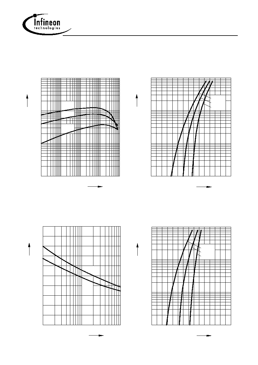
Collector cutoff current I
CBO
= f (T
A
)
V
CB
= V
CEmax
0
10
EHP00251
BCP 29/49
A
T
150
0
4
10
CBO
nA
50
100
1
10
2
10
3
10
∞C
max
typ
Total power dissipation
P
tot
= f(T
S
)
0
15
30
45
60
75
90 105 120
∞C
150
T
S
0
150
300
450
600
750
900
1050
1200
1350
mW
1650
P
tot
Transition frequency
f
T
= f (I
C
)
V
CE
= 5V
10
EHP00252
BCP 29/49
0
3
10
mA
1
10
3
10
5
10
1
10
2
10
2
C
T
f
MHz
Permissible pulse load
P
totmax
/ P
totDC
= f (t
p
)
10
EHP00253
BCP 29/49
-6
0
10
5
D =
5
10
1
5
10
2
3
10
10
-5
10
-4
10
-3
10
-2
10
0
s
0
0.005
0.01
0.02
0.05
0.1
0.2
0.5
tot max
tot
P
DC
P
p
t
t
p
=
D
T
t
p
T
BCP29, BCP49
5
Nov-29-2001
DC current gain
h
FE
= f (I
C
)
V
CE
= 5V
10
EHP00255
BCP 29/49
-1
3
10
mA
3
10
6
10
5
5
10
0
10
1
10
4
C
FE
h
2
10
5
10
∞C
125
5
25 ∞C
-55 ∞C
Collector-emitter saturation voltage
I
C
= f (V
CEsat
), h
FE
= 1000
0
10
EHP00256
BCP 29/49
CEsat
V
1.5
0
3
10
C
mA
0.5
1.0
1
10
2
10
∞C
V
5
5
150
25 ∞C
-50 ∞C
Collector-base capacitance C
CB
= f (V
CBO
)
Emitter-base capacitance
C
EB
= f (V
EBO
)
10
EHP00257
BCP 29/49
-1
1
10
V
10
0
5
10
pF
0
EB0
V
V
CB0
CB0
C
C
EB0
(
)
(
)
EB0
C
CB0
C
Base-emitter saturation voltage
I
C
= f (V
BEsat
), h
FE
= 1000
0
10
EHP00258
BCP 29/49
BEsat
V
3.0
0
3
10
C
mA
1.0
2.0
1
10
2
10
∞C
V
5
5
150
25 ∞C
-50 ∞C