BCV62
1
Jul-11-2001
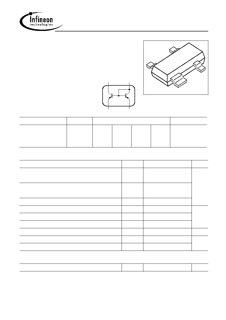
PNP Silicon Double Transistor
To be used as a current mirror
Good thermal coupling and V
BE
matching
High current gain
Low collector-emitter saturation voltage
VPS05178
2
1
3
4
EHA00013
C2 (1)
Tr.2
Tr.1
C1 (2)
E1 (3)
E2 (4)
Type
Marking
Pin Configuration
Package
BCV62A
BCV62B
BCV62C
3Js
3Ks
3Ls
1 = C2
1 = C2
1 = C2
2 = C1
2 = C1
2 = C1
3 = E1
3 = E1
3 = E1
4 = E2
4 = E2
4 = E2
SOT143
SOT143
SOT143
Maximum Ratings
Parameter
Symbol
Value
Unit
Collector-emitter voltage
(transistor T1)
V
CEO
30
V
Collector-base voltage (open emitter)
(transistor T1)
V
CBO
30
Emitter-base voltage
V
EBS
6
DC collector current
I
C
100
mA
Peak collector current
I
CM
200
Base peak current (transistor T1)
I
BM
200
Total power dissipation
, T
S
= 99 ∞C
P
tot
300
mW
Junction temperature
T
j
150
∞C
Storage temperature
T
stg
-65 ... 150
Thermal Resistance
Junction - soldering point
1)
R
thJS
170
K/W
1For calculation of R
thJA
please refer to Application Note Thermal Resistance
BCV62
2
Jul-11-2001
Electrical Characteristics at T
A
= 25∞C, unless otherwise specified
Parameter
Symbol
Values
Unit
min.
typ.
max.
DC Characteristics of T1
Collector-emitter breakdown voltage
I
C
= 10 mA, I
B
= 0
V
(BR)CEO
30
-
-
V
Collector-base breakdown voltage
I
C
= 10 µA, I
B
= 0
V
(BR)CBO
30
-
-
Emitter-base breakdown voltage
I
E
= 10 µA, I
C
= 0
V
(BR)EBO
6
-
-
Collector cutoff current
V
CB
= 30 V, I
E
= 0
I
CBO
-
-
15
nA
Collector cutoff current
V
CB
= 30 V, I
E
= 0 , T
A
= 150 ∞C
I
CBO
-
-
5
µA
DC current gain 1)
I
C
= 0.1 mA, V
CE
= 5 V
h
FE
100
-
-
-
DC current gain 1)
I
C
= 2 mA, V
CE
= 5 V
h
FE
125
220
420
180
290
520
220
475
800
Collector-emitter saturation voltage1)
I
C
= 10 mA, I
B
= 0.5 mA
I
C
= 100 mA, I
B
= 5 mA
V
CEsat
-
-
75
250
300
650
mV
Base-emitter saturation voltage 1)
I
C
= 10 mA, I
B
= 0.5 mA
I
C
= 100 mA, I
B
= 5 mA
V
BEsat
-
-
700
850
-
-
Base-emitter voltage 1)
I
C
= 2 mA, V
CE
= 5 V
I
C
= 10 mA, V
CE
= 5 V
V
BE(ON)
600
-
650
-
750
820
BCV62A
BCV62B
BCV62C
1) Pulse test: t
300
µ
s, D = 2%

BCV62
3
Jul-11-2001
Electrical Characteristics at T
A
= 25∞C, unless otherwise specified.
Parameter
Symbol
Values
Unit
min.
typ.
max.
DC Characteristics
Base-emitter forward voltage
I
E
= 10 µA
I
E
= 250 mA
V
BES
0.4
-
-
-
-
1.8
V
Matching of transistor T1 and transistor T2
at I
E2
= 0.5mA and V
CE1
= 5V
T
A
= 25 ∞C
T
A
= 150 ∞C
I
C1
/ I
C2
-
0.7
0.7
-
-
-
-
1.3
1.3
-
Thermal coupling of transistor T1 and
transistor T2
1)
T1: V
CE
= 5V
Maximum current of thermal stability of I
C1
I
E2
-
5
-
mA
AC characteristics of transistor T1
Transition frequency
I
C
= 10 mA, V
CE
= 5 V, f = 100 MHz
f
T
-
250
-
MHz
Collector-base capacitance
V
CB
= 10 V, f = 1 MHz
C
cb
-
3
-
pF
Emitter-base capacitance
V
EB
= 0.5 V, f = 1 MHz
C
eb
-
8
-
Noise figure
I
C
= 200 µA, V
CE
= 5 V, R
S
= 2 k
,
f
= 1 kHz,
f
= 200 Hz
F
-
2
-
dB
Short-circuit input impedance
I
C
= 1 mA, V
CE
= 10 V, f = 1 kHz
h
11e
-
4.5
-
k
Open-circuit reverse voltage transf.ratio
I
C
= 1 mA, V
CE
= 10 V, f = 1 kHz
h
12e
-
2
-
10
-4
Short-circuit forward current transf.ratio
I
C
= 1 mA, V
CE
= 10 V, f = 1 kHz
h
21e
100
-
900
-
Open-circuit output admittance
I
C
= 1 mA, V
CE
= 10 V, f = 1 kHz
h
22e
-
30
-
S
1) Witout emitter resistor. Device mounted on alumina 15mm x 16.5mm x 0.7mm
BCV62
4
Jul-11-2001
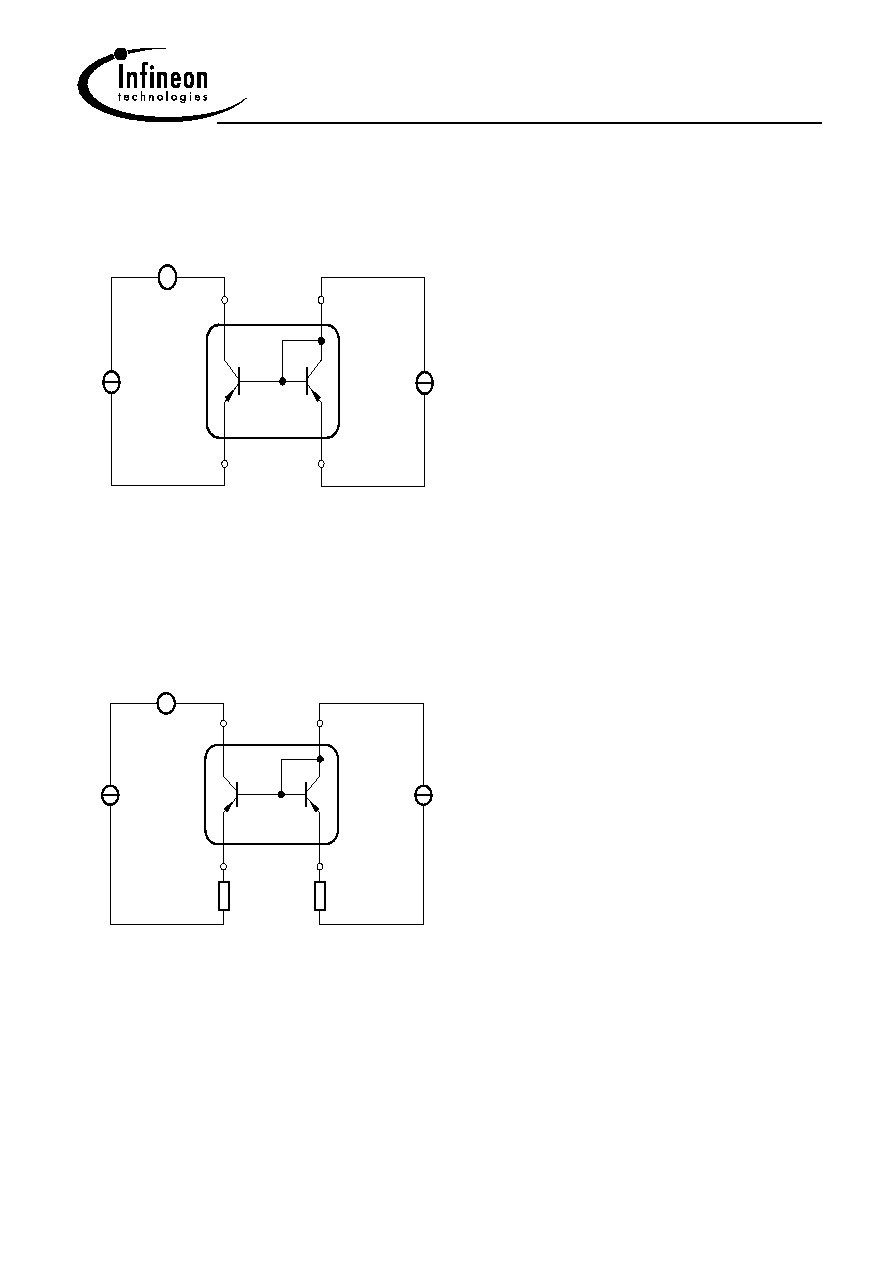
Test circuit for current matching
C1
CE1
V
A
...
CO
V
E2
EHN00003
= constant
V
CO
T2
T1
2
1
4
3
Note: Voltage drop at contacts:
V
CO
< 2/3
V
T
= 16mV
Characteristic for determination of V
CE1
at specified R
E
range with
I
E2
as parameter under condition of I
C1
/I
E2
= 1.3
EHN00004
T1
T2
...
A
2
1
4
3
V
CE1
C1
E2
= constant
R
E
R
E
Note: BCV62 with emitter resistors
BCV62
5
Jul-11-2001
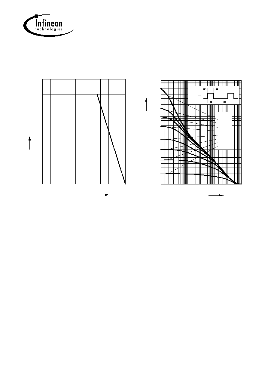
Permissible pulse load
P
totmax
/
P
totDC
=
f (t
p
)
10
EHP00941
BCV 62
-6
0
10
5
D =
5
10
1
5
10
2
3
10
10
-5
10
-4
10
-3
10
-2
10
0
s
0
0.005
0.01
0.02
0.05
0.1
0.2
0.5
tot max
tot
P
DC
P
p
t
t
p
=
D
T
t
p
T
Total power dissipation
P
tot
=
f(T
S
)
0
15
30
45
60
75
90 105 120
∞C
150
T
S
0
50
100
150
200
250
mW
350
P
tot