Feb-18-2004
2
BF1009S...
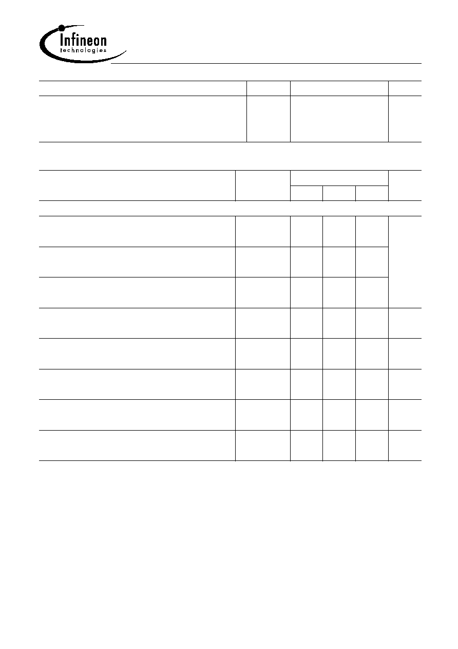
Thermal Resistance
Parameter
Symbol
Value
Unit
Channel - soldering point
1)
BF1009S, BF1009SR
BF1009SW
R
thchs
370
280
K/W
Electrical Characteristics
Parameter
Symbol
Values
Unit
min.
typ.
max.
DC Characteristics
Drain-source breakdown voltage
I
D
= 300 �A, V
G1S
= 0 , V
G2S
= 0
V
(BR)DS
12
-
-
V
Gate1-source breakdown voltage
+I
G1S
= 10 mA, V
G2S
= 0 , V
DS
= 0
+V
(BR)G1SS
8
-
12
Gate2 source breakdown voltage
�
I
G2S
= 10 mA, V
G1S
= 0 , V
DS
= 0
�
V
(BR)G2SS
10
-
16
Gate1-source leakage current
V
G1S
= 6 V, V
G2S
= 0
+I
G1SS
-
-
60
�A
Gate 2 source leakage current
�
V
G2S
= 8 V, V
G1S
= 0 , V
DS
= 0
�
I
G2SS
-
-
50
nA
Drain current
V
DS
= 9 V, V
G1S
= 0 , V
G2S
= 6 V
I
DSS
-
-
500
�A
Operating current (selfbiased)
V
DS
= 9 V, V
G2S
= 6 V
I
DSO
10
14
19
mA
Gate2-source pinch-off voltage
V
DS
= 9 V, I
D
= 100 �A
V
G2S(p)
-
0.9
-
V
1For calculation of
R
thJA
please refer to Application Note Thermal Resistance
Feb-18-2004
3
BF1009S...
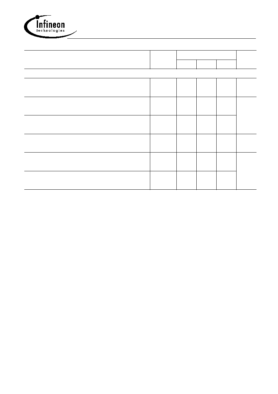
Electrical Characteristics
Parameter
Symbol
Values
Unit
min.
typ.
max.
AC Characteristics (verified by random sampling)
Forward transconductance
V
DS
= 9 V, V
G2S
= 6 V
g
fs
26
30
-
mS
Gate1 input capacitance
V
DS
= 9 V, V
G2S
= 6 V, f = 1 MHz
C
g1ss
-
2.1
2.7
pF
Output capacitance
V
DS
= 9 V, V
G2S
= 6 V, f = 1 MHz
C
dss
-
0.9
-
Power gain (self biased)
V
DS
= 9 V, V
G2S
= 6 V, f = 800 MHz
G
p
18
22
-
dB
Noise figure
V
DS
= 9 V, V
G2S
= 6 V, f = 800 MHz
F
-
1.4
2.1
dB
Gain control range
V
DS
= 9 V, V
G2S
= 6 ... 0 V, f = 800 MHz
G
p
40
50
-