BF1012S
1
Jun-28-2001
Silicon N-Channel MOSFET Tetrode
For low noise, high gain controlled
input stages up to 1GHz
Operating voltage 12V
Integrated stabilized bias network
VPS05178
2
1
3
4
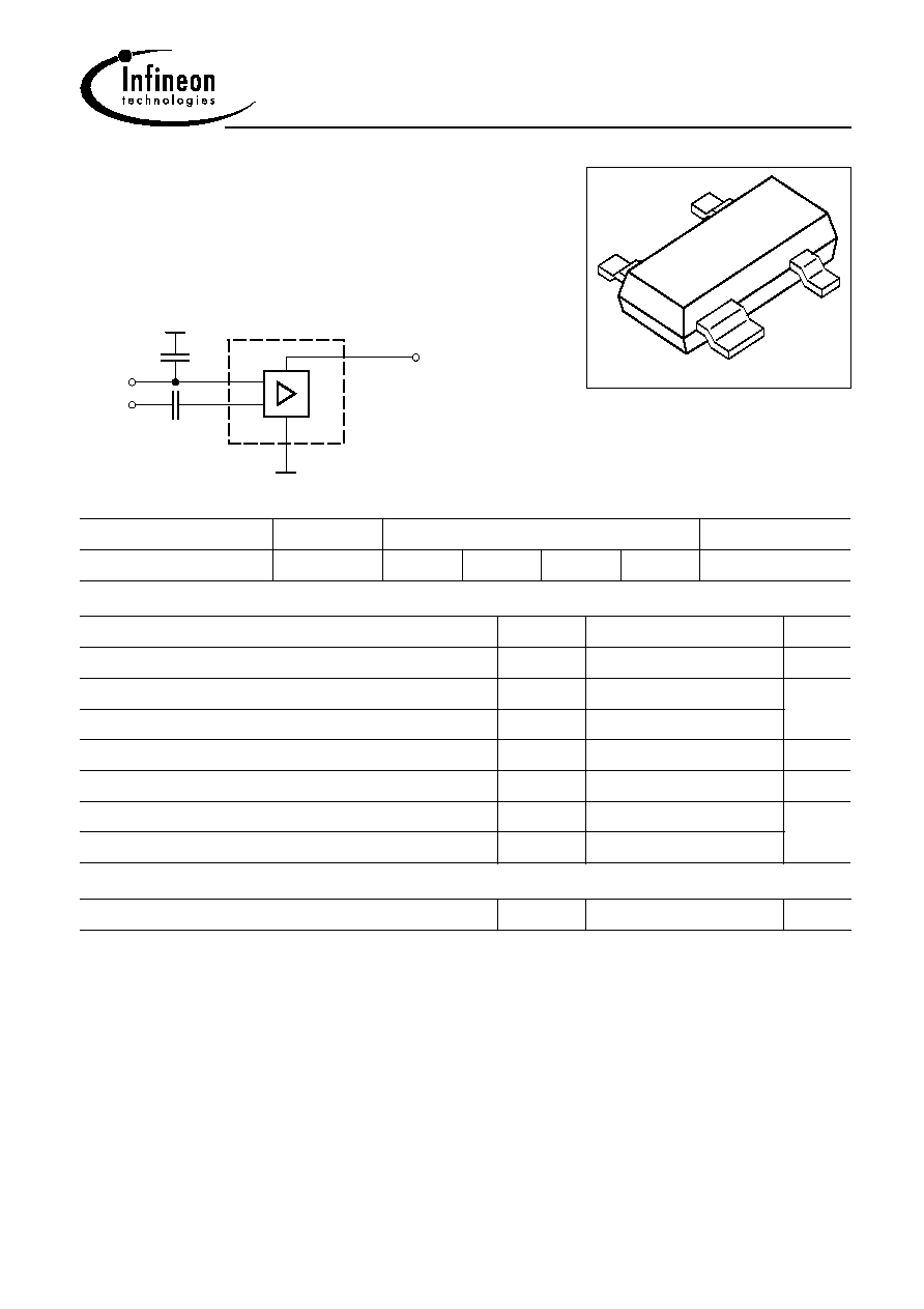
EHA07215
GND
G1
G2
Drain
AGC
HF
Input
HF Output
+ DC
ESD: Electrostatic discharge sensitive device, observe handling precaution!
Type
Marking
Pin Configuration
Package
BF1012S
NYs
1 = S
2 = D
3 = G2
4 = G1
SOT143
Maximum Ratings
Parameter
Symbol
Value
Unit
V
DS
16
Drain-source voltage
V
mA
25
I
D
Continuos drain current
Gate 1/gate 2 peak source current
10
�I
G1/2SM
+V
G1SE
3
Gate 1 (external biasing)
V
mW
P
tot
Total power dissipation
, T
S
76 �C
200
Storage temperature
�C
-55 ... 150
T
stg
T
ch
150
Channel temperature
Thermal Resistance
Channel - soldering point
1)
R
thchs
370
K/W
1For calculation of R
thJA
please refer to Application Note Thermal Resistance
Note:
It is not recommended to apply external DC-voltage on Gate 1 in active mode.

BF1012S
2
Jun-28-2001
Electrical Characteristics at T
A
= 25�C, unless otherwise specified.
Parameter
Symbol
Values
Unit
min.
typ.
max.
DC characteristics
Drain-source breakdown voltage
I
D
= 300 �A, V
G1S
= 0 V, V
G2S
= 0 V
V
-
V
(BR)DS
-
16
Gate 1 - source breakdown voltage
+I
G1S
= 10 mA, V
G2S
= 0 V, V
DS
= 0 V
-
12
+V
(BR)G1SS
8
Gate 2 source breakdown voltage
�I
G2S
= 10 mA, V
G1S
= 0 V, V
DS
= 0 V
-
16
10
�V
(BR)G2SS
Gate 1 source current
V
G1S
= 6 V, V
G2S
= 0 V
-
-
�A
60
+I
G1SS
Gate 2 source leakage current
�V
G2S
= 8 V, V
G1S
= 0 V, V
DS
= 0 V
�I
G2SS
-
-
nA
50
I
DSS
-
500
�A
-
Drain current
V
DS
= 12 V, V
G1S
= 0 , V
G2S
= 6 V
I
DSO
8
12
Operating current (selfbiased)
V
DS
= 12 V, V
G2S
= 6 V
mA
-
V
G2S(p)
-
0.9
-
V
Gate 2-source pinch-off voltage
V
DS
= 12 V, I
D
= 100 �A
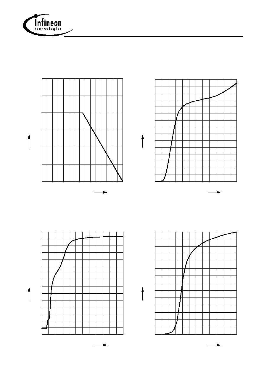
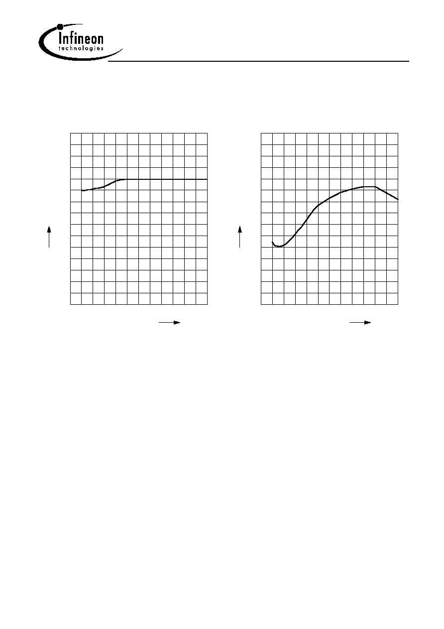
AC characteristics
Forward transconductance (self biased)
V
DS
= 12 V, V
G2S
= 6 V
g
fs
26
30
-
mS
Gate 1-input capacitance (self biased)
V
DS
= 12 V, V
G2S
= 6 , f = 1 MHz
C
g1ss
-
2.1
2.7
pF
Output capacitance (self biased)
V
DS
= 12 V, V
G2S
= 6 , f = 1 MHz
C
dss
-
0.9
-
Power gain (self biased)
V
DS
= 12 V, V
G2S
= 6 , f = 800 MHz
G
ps
18
22
-
dB
Noise figure (self biased)
V
DS
= 12 V, V
G2S
= 6 , f = 800 MHz
F
800
-
1.4
-
dB
Gain control range (self biased)
V
DS
= 12 V, VG2S = 6 ... 0V, f = 800 MHz
G
ps
40
50
-