Apr-23-2004
1
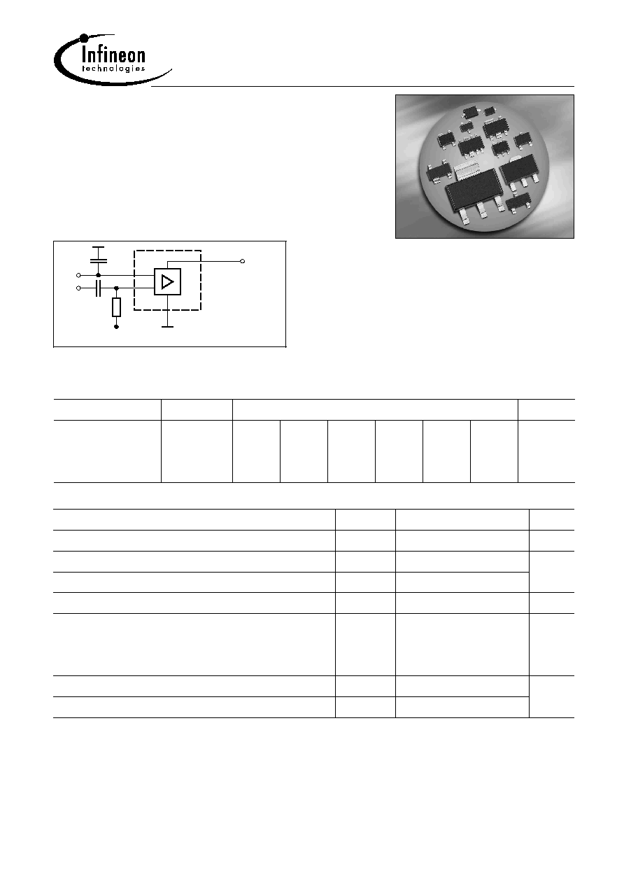
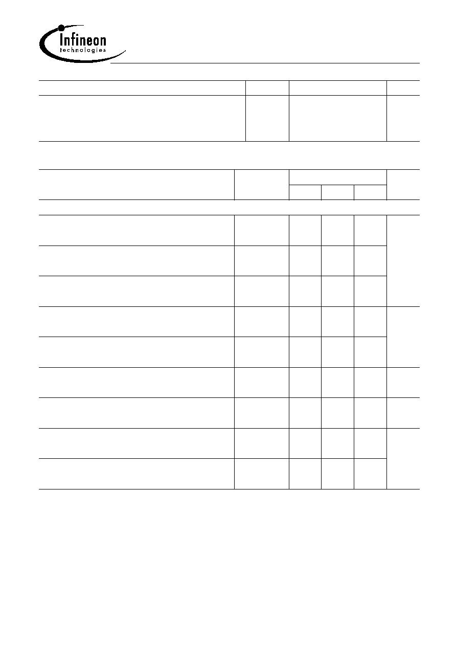
BF2030...
Silicon N-Channel MOSFET Tetrode
∑
For low noise, high gain controlled
input stages up to 1GHz
∑
Operating voltage 5V
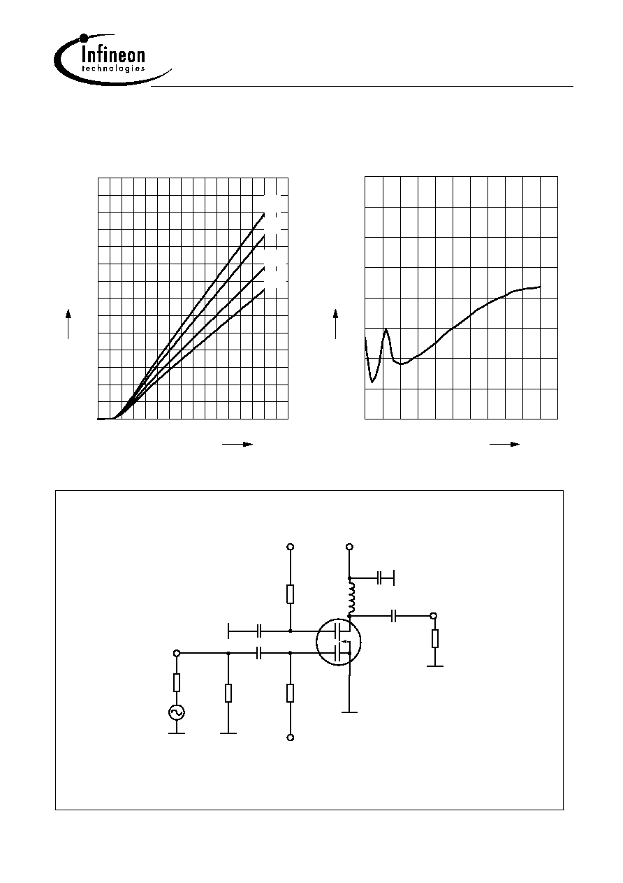
EHA07461
GND
G1
G2
Drain
AGC
HF
Input
HF Output
+ DC
GG
V
G1
R
ESD
: Electrostatic discharge sensitive device, observe handling precaution!
Class 2 (2000V - 4000V) pin to pin Human Body Model
Type
Package
Pin Configuration
Marking
BF2030
BF2030R
BF2030W
SOT143
SOT143R
SOT343
1= S
1= D
1= D
2=D
2=S
2=S
3=G2
3=G1
3=G1
4=G1
4=G2
4=G2
-
-
-
-
-
-
NDs
NDs
ND
Maximum Ratings
Parameter
Symbol
Value
Unit
Drain-source voltage
V
DS
8
V
Continuous drain current
I
D
20
mA
Gate 1/ gate 2-source current
±
I
G1/2SM
10
Gate 1 (external biasing)
+V
G1SE
6
V
Total power dissipation
T
S
76 ∞C, BF2030, BF2030R
T
S
94 ∞C, BF2030W
P
tot
200
200
mW
Storage temperature
T
stg
-55 ... 150
∞C
Channel temperature
T
ch
150
Apr-23-2004
2
BF2030...
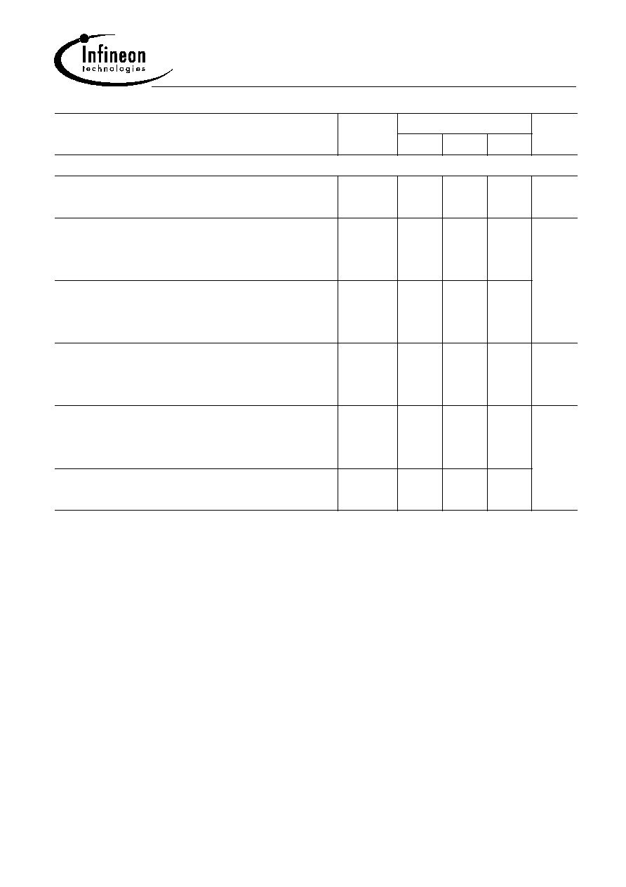
Thermal Resistance
Parameter
Symbol
Value
Unit
Channel - soldering point
1)
BF2030/ BF2030R
BF2030W
R
thchs
370
280
K/W
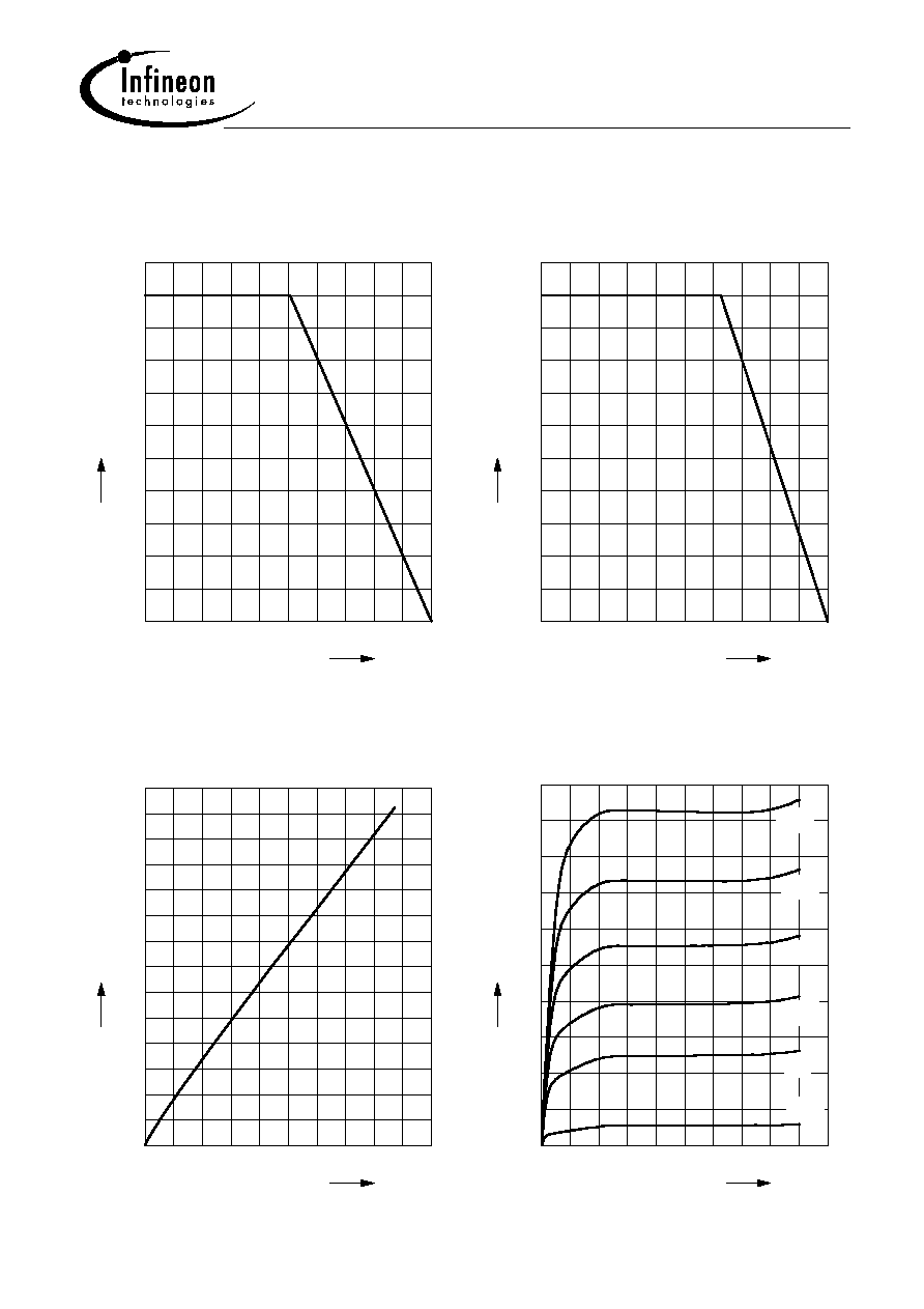
Electrical Characteristics
Parameter
Symbol
Values
Unit
min.
typ.
max.
DC Characteristics
Drain-source breakdown voltage
I
D
= 20 µA, V
G1S
= 0 , V
G2S
= 0
V
(BR)DS
10
-
-
V
Gate1-source breakdown voltage
+I
G1S
= 10 mA, V
G2S
= 0 , V
DS
= 0
+V
(BR)G1SS
6
-
15
Gate2-source breakdown voltage
+I
G2S
= 10 mA, V
G1S
= 0 , V
DS
= 0
+V
(BR)G2SS
6
-
15
Gate1-source leakage current
V
G1S
= 5 V, V
G2S
= 0 , V
DS
= 0
+I
G1SS
-
-
50
nA
Gate2-source leakage current
V
G2S
= 5 V, V
G1S
= 0 , V
DS
= 0
+I
G2SS
-
-
50
Drain current
V
DS
= 5 V, V
G1S
= 0 , V
G2S
= 4 V
I
DSS
-
-
50
µA
Drain-source current
V
DS
= 5 V, V
G2S
= 4 V, R
G1
= 100
k
I
DSX
-
12
-
mA
Gate1-source pinch-off voltage
V
DS
= 5 V, V
G2S
= 4 V, I
D
= 20 µA
V
G1S(p)
0.3
0.5
-
V
Gate2-source pinch-off voltage
V
DS
= 5 V, I
D
= 20 µA
V
G2S(p)
0.3
0.6
-
1For calculation of
R
thJA
please refer to Application Note Thermal Resistance
Apr-23-2004
3
BF2030...
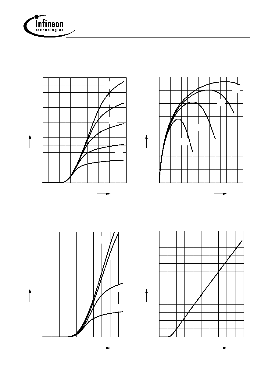
Electrical Characteristics
Parameter
Symbol
Values
Unit
min.
typ.
max.
AC Characteristics (verified by random sampling)
Forward transconductance
V
DS
= 5 V, I
D
= 10 mA, V
G2S
= 4 V
g
fs
27
31
-
mS
Gate1 input capacitance
V
DS
= 5 V, I
D
= 10 mA, V
G2S
= 4 V,
f = 1 MHz
C
g1ss
-
2.4
2.8
pF
Output capacitance
V
DS
= 5 V, I
D
= 10 mA, V
G2S
= 4 V,
f = 1 MHz
C
dss
-
1.3
-
Power gain
V
DS
= 5 V, I
D
= 10 mA, V
G2S
= 4 V,
f = 800 MHz
G
p
20
23
-
dB
Noise figure
V
DS
= 5 V, I
D
= 10 mA, V
G2S
= 4 V,
f = 800 MHz
F
-
1.5
2.2
dB
Gain control range
V
DS
= 5 V, V
G2S
= 4...0 V, f = 800 MHz
G
p
40
50
-