 | ÐлекÑÑоннÑй компоненÑ: BFG235 | СкаÑаÑÑ:  PDF PDF  ZIP ZIP |
Äîêóìåíòàöèÿ è îïèñàíèÿ www.docs.chipfind.ru
BFG 235
Oct-27-1999
1
NPN Silicon RF Transistor
For low-distortion broadband output amplifier
stages in antenna and telecommunication
systems up to 2 GHz at collector currents from
120 mA to 250 mA
Power amplifiers for DECT and PCN systems
Integrated emitter ballast resistor
f
T
= 5.5 GHz
VPS05163
1
2
3
4
ESD
: Electrostatic discharge sensitive device, observe handling precaution!
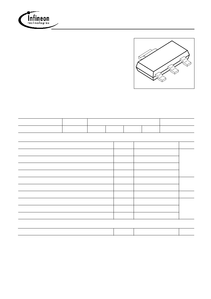
Type
Marking
Pin Configuration
Package
BFG 235
BFG235
1 = E
2 = B
3 = E
4 = C
SOT-223
Maximum Ratings
Parameter
Symbol
Value
Unit
Collector-emitter voltage
V
CEO
15
V
Collector-emitter voltage
V
CES
25
Collector-base voltage
V
CBO
25
Emitter-base voltage
V
EBO
2
Collector current
I
C
300
mA
Base current
I
B
40
Total power dissipation
, T
S
80 °C
F)
P
tot
2
W
Junction temperature
T
j
150
°C
Ambient temperature
T
A
-65 ... 150
Storage temperature
T
stg
-65 ... 150
Thermal Resistance
Junction - soldering point
R
thJS
35
K/W
1T
S
is measured on the collector lead at the soldering point to the pcb
BFG 235
Oct-27-1999
2
Electrical Characteristics at T
A
= 25°C, unless otherwise specified.
Parameter
Symbol
Values
Unit
min.
typ.
max.
DC characteristics
Collector-emitter breakdown voltage
I
C
= 1 mA, I
B
= 0
V
(BR)CEO
15
-
-
V
Collector-emitter cutoff current
V
CE
= 25 V, V
BE
= 0
I
CES
-
-
200
µA
Collector-base cutoff current
V
CB
= 10 V, I
E
= 0
I
CBO
-
-
100
nA
Emitter-base cutoff current
V
EB
= 1 V, I
C
= 0
I
EBO
-
-
2
µA
DC current gain
I
C
= 200 mA, V
CE
= 8 V
h
FE
50
120
250
-

BFG 235
Oct-27-1999
3
Electrical Characteristics at T
A
= 25°C, unless otherwise specified.
Parameter
Symbol
Values
Unit
min.
typ.
max.
AC characteristics
(verified by random sampling)
Transition frequency
I
C
= 200 mA, V
CE
= 8 V, f = 200 MHz
f
T
4
5.5
-
GHz
Collector-base capacitance
V
CB
= 10 V, f = 1 MHz
C
cb
-
2.6
3.6
pF
Collector-emitter capacitance
V
CE
= 10 V, f = 1 MHz
C
ce
-
1.5
-
Emitter-base capacitance
V
EB
= 0.5 V, f = 1 MHz
C
eb
-
15
-
Noise figure
I
C
= 60 mA, V
CE
= 8 V, Z
S
= Z
Sopt
,
f
= 900 MHz
F
-
2.7
-
dB
Power gain, maximum available
F)
I
C
= 200 mA, V
CE
= 8 V, Z
S
= Z
Sopt
, Z
L
= Z
Lopt
,
f
= 900 MHz
G
ma
-
12
-
Transducer gain
I
C
= 200 mA, V
CE
= 8 V, Z
S
= Z
L
= 50
,
f
= 900 MHz
|S
21e
|
2
-
6
-
Third order intercept point
I
C
= 200 mA, V
CE
= 8 V, Z
S
= Z
L
= 50
,
f
= 900 MHz
IP
3
-
40
-
dBm
1
G
ma
= |S
21
/ S
12
| (k-(k
2
-1)
1/2
)
BFG 235
Oct-27-1999
4
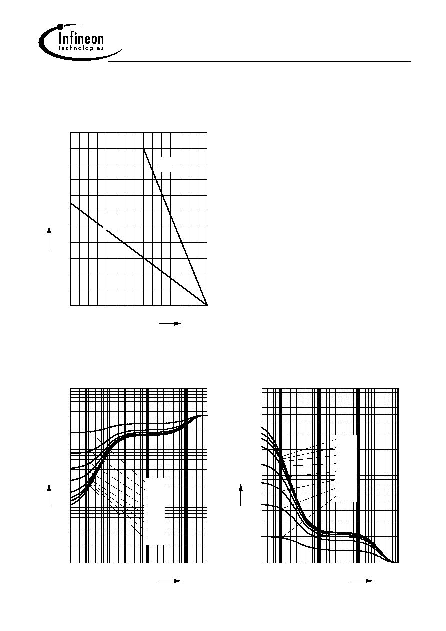
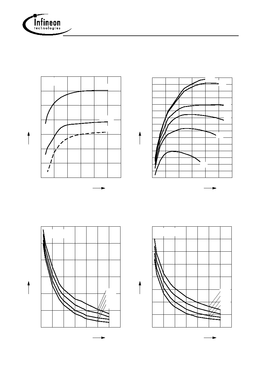
Total power dissipation P
tot
= f (T
A
*, T
S
)
* Package mounted on epoxy
0
20
40
60
80
100
120 °C
150
T
A
,T
S
0
200
400
600
800
1000
1200
1400
1600
1800
mW
2200
P
tot
T
S
T
A
Permissible Pulse Load R
thJS
= f (t
p
)
10
-7
10
-6
10
-5
10
-4
10
-3
10
-2
10
0
s
t
p
-1
10
0
10
1
10
2
10
K/W
R
thJS
0.5
0.2
0.1
0.05
0.02
0.01
0.005
D = 0
Permissible Pulse Load
P
totmax
/P
totDC
= f (t
p
)
10
-7
10
-6
10
-5
10
-4
10
-3
10
-2
10
0
s
t
p
0
10
1
10
2
10
-
P
tot
m
ax
/ P
totDC
D = 0
0.005
0.01
0.02
0.05
0.1
0.2
0.5
BFG 235
Oct-27-1999
5
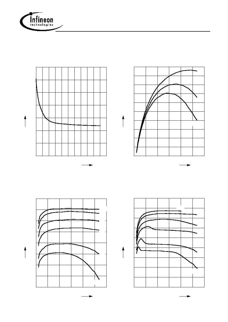
Collector-base capacitance C
cb
= f (V
CB
)
f = 1MHz
0
4
8
12
16
V
22
V
CB
0
1
2
3
4
5
pF
7
C
cb
Transition frequency f
T
= f (I
C
)
V
CE
= Parameter
0
50
100
150
200
mA
300
I
C
1.0
1.5
2.0
2.5
3.0
3.5
4.0
4.5
5.0
GHz
6.0
f
T
1V
0.7V
5V
Power Gain G
ma
, G
ms
= f(I
C
)
f = 0.9GHz
V
CE
= Parameter
0
50
100
150
200
mA
300
I
C
5
6
7
8
9
10
11
dB
13
G
10V
5V
3V
2V
1V
0.7V
Power Gain G
ma
, G
ms
= f(I
C
)
f = 1.8GHz
V
CE
= Parameter
0
50
100
150
200
mA
300
I
C
0
1
2
3
4
5
6
7
dB
9
G
10V
5V
3V
2V
1V
0.7V
BFG 235
Oct-27-1999
6
Power Gain G
ma
, G
ms
= f(V
CE
):_____
|S
21
|
2
= f(V
CE
):---------
f = Parameter
0
2
4
6
8
V
12
V
CE
0
2
4
6
8
10
dB
14
G
0.9GHz
1.8GHz
0.9GHz
I
C
=200mA
Intermodulation Intercept Point IP
3
=f(I
C
)
(3rd order, Output,
Z
S
=Z
L
=50
)
V
CE
= Parameter, f = 900MHz
0
50
100
150
200
mA
300
I
C
12
14
16
18
20
22
24
26
28
30
32
34
36
dBm
42
IP
3
10V
8V
5V
3V
2V
1V
Power Gain G
ma
, G
ms
= f(f)
V
CE
= Parameter
0.0
0.5
1.0
1.5
2.0
2.5
GHz
3.5
f
0
5
10
15
20
dB
30
G
I
C
=200mA
10V
2V
1V
0.7V
Power Gain |S
21
|
2
= f(f)
V
CE
=
Parameter
0.0
0.5
1.0
1.5
2.0
2.5
GHz
3.5
f
-10
-5
0
5
10
15
20
dB
30
S
21
I
C
=200mA
10V
2V
1V
0.7V